
Worklog LumaDoub: An Open Source Line-Doubler and Transcoder

The ADV7390 has a "SD progressive" mode, which what us gamers refer to as "240p". As you can assume, when this is selected, it makes the chip output 240p, which is 480i without alternating fields. If you send a 240p signal into this chip, and do not enable this mode, the outgoing 240p signal will have many issues. So this bit must be enabled when the signal is receiving a 240p signal.

Prior to today, I was toggling this mode manually. Today, we were able to use a register in the ADV7280A to detect if the signal is progressive 240p or interlaced 480i, and toggle it automatically.

Additionally, if you send this chip 480i, and then enable this mode, the fields will not alternating, turning it into 240p. This "force 240p" is a neat feature useful for many niche circumstances, so I will keep it as a feature. It will enable automatically for 240p sources, but can be manually enabled for 480i sources.


Line doubling works, but currently looks like garbage. 240p signals bounce up and down; it looks like the chip is attempting to deinterlace the 240p signal. But the chip is supposed to use simple bob deinterlacing so I'm not really sure what's going on. I will have to explore flipping more bits.

I have yet to figure out how to toggle the 480p smoothing filter(s). This wouldn't be too tragic, except it is currently stuck in the "ON" position. I tried toggling the obvious registers the datasheet lays out, but none of them seem to do the trick. This one is proving much tricker than I anticipated. Fortunately, it only appears to affect 480p outputs; 240p and 480i look quite sharp.

The core transcoder portion of this project is pretty close to feature complete. The line doubling to 480p, on the other hand, still has a ways to go.

I do have some bad news: it appears my "RGB passthrough" idea will not work. The output is quite green, and my scope showed that the "Blue" (actually pb) and "Red" (actually pr) outputs have a .35v peak rather than the intended .7v peak that "Green" (actually Y) has. This makes sense though. There may be a way to attenuate or amplify the signal to correct for this, but we may just have to just throw a transcoder circuit on the input stage. PXL_20250214_095654795.jpg
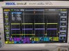
 
I hoped it wasn't too good to be true, regarding RGsB over YPbPr!

Still waiting on components myself so I can't test anything and just excitedly watch you... But OpAmp(s) with a gain of 2x should do it dont ya think?
 
I hoped it wasn't too good to be true, regarding RGsB over YPbPr!

Still waiting on components myself so I can't test anything and just excitedly watch you... But OpAmp(s) with a gain of 2x should do it dont ya think?
Potentially, but I worry it may be a -.35v to +.35v swing rather than a 0v to .7v swing at half amplitude, as pb/pr are differential signals. Would need to do something a little more complicated. Pretty tricky. All else fails, I can stick an analog transcoder circuit on the input stage.
 
Ahhh I see. Right on, I'd always thought I was going to have to add a transcoder, until I learned of your trick idea.
 
After many late nights of troubleshooting to no success, the line doubled output still looked awful. So I reached out to the ADV7280A man himself: Mike Chi of RetroTink. I knew he would have the answers, but he's a busy man and I wanted to wait to reach out to him until I reached the end of what I could do on my own.

He was extremely friendly, and told me about a secret undocumented register on the chip. I flipped 2 bits, and the rounded edges of my N64 composite signal sharpened up.

Before:
PXL_20250227_232926913.jpg

After:
PXL_20250227_232916856.jpg

Ah-Ha! A huge improvement! This is what I had been looking for. But what you can't see in the photo is it was still treating the input signal like 480i instead of 240p; bobbing the image up and down. I asked Mike, and again he had the answer: Flip a bit to enable "Fast lock" mode. Once I did that, the 480p line doubled output was sharp and steady.

Fast Lock (smoothing disabled)
PXL_20250228_031721764.jpg


Fast lock (smoothing enabled)
PXL_20250228_032233020.jpg


Not bad for a stock N64 via composite! The output is 480p RGB into a BVM-D9.

And of course, for those of you like me concerned with latency...
PXL_20250228_040637500.jpg


And with that, the first iteration of lumadoub is near feature complete. I have a few more minor features I would like to do, then my partner and I shall (but mostly her because she's actually competent at writing code) overhaul the code to make it tidy, organized, and documented prior to release.

Excited to release this. Note that this release will be a toolkit to design and create your own lumadoub boards; not a standalone product you can buy or a ready-to-populate board.
 
Last edited:
I had an idea to implement artificial scanlines with no additional hardware by turning the DACs on and off every line. I ran the hsync line back to a gpio of the pico, and ran an interrupt to send an i2c command to toggle the red and blue DACs on and off every hsync pulse. (Note: I left the green dac on, as it carried sync, but muted it on the monitor.)

Here was the result:
PXL_20250301_090537339~2.jpg

I enjoy some thick scanlines, but not quite like this. My guess is the 400khz i2c bus just isn't fast enough to toggle the lines at 31khz, especially with overhead.

Seems this avenue was a dead end, but I'm not giving up on artificial scanlines just yet. I am going to explore additional methods, but unfortunately, they will likely require the use of additional components.
 
My guess is the 400khz i2c bus just isn't fast enough to toggle the lines at 31khz

Unfortunately I think this is it. Even with zero overhead you won't be able to clock out the i2c commands fast enough. Assuming this is standard-ish 3 byte i2c payload of [target address][register address][register value], thats 29 bits of data (3 bytes + acks + starts and stops). Clocking this out 31k times per second adds up to ~900k bits per second. Someone check my math though :)

This project is still badass without the "extra credit" of onboard scanlines though :)
 
Artificial scanlines are proving to be much more difficult than I anticipated. Since pure software isn't an option, I have been experimenting with hardware solutions.

The principle of artificial scanlines is simple: every other line, the line is totally black. On paper, this should be simple, as in the analog video domain, 0v is minimum brightness, and .7v is maximum brightness. So if you had .7v on red, green, and blue, you would have white.

Easy, just short it to ground when we want the signal to be blacked out, right? That's what I suspected but, no, it's not that simple.
Here's is a test pattern I put up on the screen, and here is what each line looks like on the oscilloscope.
PXL_20250303_020808777.jpg

PXL_20250303_020202748.jpg

As you can see here, black is NOT at 0v. Because normally, a signal goes negative voltage to signify it is in a blanking period. However, this chip is only powered by a positive voltage source, and not a negative voltage source, so it can not generate a negative voltage. So instead, it offsets the entire signal, shifting the entire signal vertically on the scope.

So this means grounding the signals isn't an option. So what about switching them off entirely? I tried wiring up a ths7374, a popular video buffer/amplifier in the retro gaming world, that has a convenient disable pin. I used the rp2040 to toggle the disable pin (and therefore the output of the chip) every line.

PXL_20250302_035143138.MP.jpg

Hey that looks pretty good right? Unfortunately, there are still problems. The signal without artificial scanlines looked fine, but the brightness went crazy high when I turned on the artificial scanlines. I had to crank my monitors brightness way down to get this signal. The output was way too bright.

I put the test pattern from before through the ths7374 into the scope...
PXL_20250303_020303591~2.jpg

Looks fine. Same wave as before, with a DC bias.

Let's see the test pattern with artificial scanlines:
PXL_20250303_020643390.jpg

So the voltage during the "artificial scan line" (when the tha7374 is off) is much higher than the black level while it's on. I suspect this is the issue that's throwing the whole level completely off. My other suspicion is the timing of me cutting off the signal may be off, and is messing with the blanking interval when I'm cutting off the signal. There's als a pretty nasty transient spike on the transition, likely due to an impedance mismatch.

And finally, I did try AC coupling the signal to remove the DC bias, to no success.
PXL_20250303_021515882.jpg


This is a tricky one. I'm going to have to think on a solution to add this feature without substantially increasing the BOM.
 
After many late nights of troubleshooting to no success, the line doubled output still looked awful. So I reached out to the ADV7280A man himself: Mike Chi of RetroTink. I knew he would have the answers, but he's a busy man and I wanted to wait to reach out to him until I reached the end of what I could do on my own.

He was extremely friendly, and told me about a secret undocumented register on the chip. I flipped 2 bits, and the rounded edges of my N64 composite signal sharpened up.

Before:
View attachment 37739
After:
View attachment 37740
Ah-Ha! A huge improvement! This is what I had been looking for. But what you can't see in the photo is it was still treating the input signal like 480i instead of 240p; bobbing the image up and down. I asked Mike, and again he had the answer: Flip a bit to enable "Fast lock" mode. Once I did that, the 480p line doubled output was sharp and steady.

Fast Lock (smoothing disabled)
View attachment 37741

Fast lock (smoothing enabled)
View attachment 37742

Not bad for a stock N64 via composite! The output is 480p RGB into a BVM-D9.

And of course, for those of you like me concerned with latency...
View attachment 37743

And with that, the first iteration of lumadoub is near feature complete. I have a few more minor features I would like to do, then my partner and I shall (but mostly her because she's actually competent at writing code) overhaul the code to make it tidy, organized, and documented prior to release.

Excited to release this. Note that this release will be a toolkit to design and create your own lumadoub boards; not a standalone product you can buy or a ready-to-populate board.
That's really great, I'd like to ask you what the unrecorded registers are that you mentioned, if that's handy.
By the way, I would like to ask you a question, when outputting NTSC video with the I2P function turned off, a part of the screen is missing at the top, I don't know if you have encountered this problem.
Whether you answer or not, I would like to thank you.
 
That's really great, I'd like to ask you what the unrecorded registers are that you mentioned, if that's handy.

It is within the VPP map (0x42) of the ADV7280 and ADV7280A. The register is 0x5A. You want to set bits 3 and 4 to 0 to disable the smoothing filter and enable simple line doubling.

So as an example:
0x42, 0x5A, 0b00011010 - Default values for the register. "Smoothing" line doubling behavior
0x42, 0x5A, 0b00000010 - Simple line doubling with smoothing disabled

Additionally, for 240p (SD progressive) input to be recognized properly as 240p rather than 480i, you want to enable fast lock. It is in a register called "FL control" within the "User Sub Map 2" address. To enter Sub map 2, you need to set 0xE to 0x40. Then, after performing the command within sub map 2, you need to return to sub map 1 by changing 0x0E back to 0x84. So you would need to do the following commands:

0x20, 0x0E, 0x40 - Enter sub map 2
0x20, 0xE0, 0x01 - Enable fast lock mode to fix 240p (within sub map 2)
0x20, 0x0E, 0x84 - Leave sub map 2 (returns to sub map 1)

Shoutouts to Mike Chi of RetroTink for this information.

By the way, I would like to ask you a question, when outputting NTSC video with the I2P function turned off, a part of the screen is missing at the top, I don't know if you have encountered this problem.
I have not encountered this problem before.
 
Last edited:
Hello,

are there any updates regarding to 240p RGsB to 480p RGsB?
 
Hello,

are there any updates regarding to 240p RGsB to 480p RGsB?

I spent a stupid amount of hours investigating avenues for native RGB input. I'm like 95% sure the chip can do it in one of 2 different ways, but the feature is locked out.

Instead I'm taking the approach of adding an RGB to YPbPr transcoder for the input stage. It pretty much doubles the pcb area and part count, but it only adds like $2 to the BoM... Assuming it works properly. Still need to finish it. If it works, should be able to do RGBS, RGBHV, sync on luma/composite, 75r and ttl.

For SoG specifically, I dont know the optimal way to add it. Sending SoG into the transcoder "works" and displays a picture, but the image has a really strong green tint, likely due to the offset of the green level. RsGsBs works without issue, but I'm not sure if I will be able to find a working solution for SoG. I'll test it on the new circuit once I finish it.
 
Thank you for efforts, I am looking forward to it. There are a lot of cars with 240p navigation systems and your project can make it possible various upgrades. I think with your setup and a little modification 480p LCD's can be used instead of 240p ones.
 
  • Like
Reactions: Y2K
It is within the VPP map (0x42) of the ADV7280 and ADV7280A. The register is 0x5A. You want to set bits 3 and 4 to 0 to disable the smoothing filter and enable simple line doubling.

So as an example:
0x42, 0x5A, 0b00011010 - Default values for the register. "Smoothing" line doubling behavior
0x42, 0x5A, 0b00000010 - Simple line doubling with smoothing disabled

Additionally, for 240p (SD progressive) input to be recognized properly as 240p rather than 480i, you want to enable fast lock. It is in a register called "FL control" within the "User Sub Map 2" address. To enter Sub map 2, you need to set 0xE to 0x40. Then, after performing the command within sub map 2, you need to return to sub map 1 by changing 0x0E back to 0x84. So you would need to do the following commands:

0x20, 0x0E, 0x40 - Enter sub map 2
0x20, 0xE0, 0x01 - Enable fast lock mode to fix 240p (within sub map 2)
0x20, 0x0E, 0x84 - Leave sub map 2 (returns to sub map 1)

Shoutouts to Mike Chi of RetroTink for this information.


I have not encountered this problem before.
Thank you for this. I can confirm that the registry value does something on 7180 also. i have that eval board you showed with the 7180a version of the chip. I got my composite n64 playing rouge squadron with expanded memory correctly now. let me know if you like to me to help test anything.
 
2 years later, I have decided to release what I have of the project.


The project was a collaborative effort between my partner and I. However, her transition from "Unemployed Software Engineer" to "Employed Software Engineer" put a damper on things, and other projects piling up on my plate pushed this project to the backburner. Rather than let it sit and rot, I am releasing what I had so maybe someone else can pick up the torch. She was able to get it to a functional-but-incomplete state at one point, and I began making a mess to experiment with exploring capabilities and additional features. Assume everything functional and well documented was done by her, and everything broken, nonsensical, and poor practice is done by me. Most of the hard work/documentation is there, and I suspect a competent software or embedded engineer could pretty easily rebuild a new codebase using this as a reference. Hell, maybe even a few LLM prompts could do it.

I genuinely hope someone picks up the torch on this project, and if someone wants to, please reach out. I would be happy to help guide you through it.

For now, I'm going to leave you with a dump of what I can remember...

Explanation of the codebase to the best of my knowledge:
The device is essentially a state machine; it reads the state of 8 input switches, and based on those input switches, it sends i2c commands to the ADV7280A (input chip) and ADV7391 (output chip). The 2 chips are rather finicky, and requires a rather specific set of startup commands (included in the code) in order to start up the chips. After that, it reads the state of the switches, and sends commands to the chip when the switches are flipped. The commands for each of the inputs, outputs, and modifications (line doubling, smoothing, cvbs comb filter, force 240p, etc) are all present, functional, and should be correct. Its really that simple; read the state of the switches, and send the registers I have documented. The hard and tedious work is done; I simply lack the software prowess to implement a proper state machine for the documented states.

The ADV7280A has a few tricky things to watch out for. It has more than one device address, AND one of the addresses has more than one "page" of registers. One register is set to select which page you are accessing, so it needs to be toggled. We got this working in the code, and details are in the datasheet.

One stretch feature I was working on was auto input detection, which I recall I had *mostly* working. I wanted to make it be able to detect if you had composite, component, or svideo plugged in, by cycling through the inputs, until it locked onto an input. There are a few ways to do this; I believe I did it by having the sync carrying input for each video type (composite, luma for svideo, and luma for component) run to a different input, (which I set using the analog front end muxes, AFE, configurable using registers), and checked for hlock and vlock. As a result, for the 4 input pins, it probably doesn't currently have the default current input pin order. You can likely be more logical about shared input pins by utilizing the chroma lock to detect the presence of svideo and composite. This feature is completely optional, and all it does is let you not have to flip switches when you want to manually change input types between composite, svideo, or component.

The second stretch feature I wanted was RGB input. There are 2 ways to do this; with an external transcoder circuit (and possibly a mux), and on the chip itself. Ideally, doing it though the chip would be idea, but the chip does not say it can do it. I'm almost certain the functionality is still on the chip somewhere, but the amount of effort I put into searching is part of what burnt me out on the project. Analog Devices support is absolutely beyond useless. You may see remains of my attempts messing up the code. I would advise abandoning trying to find onboard RGB.

The third stretch feature I wanted to implement was artificial scanlines by blanking every other line. I tried a few times, and didn't find a solution I liked. You may find some leftover mess from it.

HARDWARE:
The hardware is pretty simple. The ADV7280A accepts 480i/240p composite, svideo, or YPbPr, and outputs BT.656. The ADV7391 accepts BT.656, and outputs Composite+svideo, YPbPr, or RGB at 240p/480i/480p. This makes it effectively a universal converter between these video types. At a minimum, you need these 2 chips, their supplimentary components, voltage regulation, and a microcontroller that can read switches to send i2c commands. The components in the silkscreen rectangle and the 3 passives per input to the left of the rectangle are really all you need for the chips, aside from power and an mcu.

My dev board is a bit overkill. It has 2 raspberry picos; one for the main MCU, and one to act as an attached programmer/debugger. In addition to the 8 switches, I also included another 8 to experiment with flipping bits, and A/B testing. Onboard regulators are overkill. They are designed by @YveltalGriffin so I can measure the current on each rail/chip independently. Regs are connected with jumpers to experiment with merging various lines together to assess reduction to a more sensible BoM. Input and output on the top are 2 DE15 (vga) connectors. The 4 analog inputs to the ADV7280 are connected to the R, G, B and H pins. The 3 outputs of the ADV7391 run to the RGB pins of the other connector; the H and V pins can be connected to few different pins via jumpers. I put jumpers and headers pretty much everywhere to ease the testing. The big header on the top allows you to tap almost everything.

On the left side of the PCB I have a transcoder circuit, taken from this open source transcoder by Jam.
Input to it is the DE15 connector on the side. It is completely optional, separated by jumpers, and while it should work, I did not test it.


Anyways, sorry I wasn't able to see this project to completion, especially given it's so close to the finish line. I hope someone else will pick up the torch, and I would be happy to answer questions and help those who want to. Would love to see it be completed some day.
 
Back
Top