Board scan Virtual Boy Board Scans

Shank

Moderator
Staff member
.
.
Joined
Jan 31, 2016
Messages
1,365
Likes
2,956
Portables
6
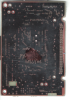
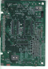
A while back, I acquired a completely toasted Virtual Boy motherboard. I finally got around to blasting the components off of it, sanding, and scanning. I have scanned the surface layers, but not the internals. I may get to that one day...
-I'm like 90% sure there is only one revision of the board
-I suspect the board is 4 layers.
-A single pad was lifted, but the trace connected to the pad is clearly visible

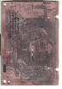
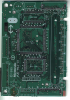
Lower res screenshots:
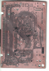
Fk8nSaE.png
A0h9KHz.png

FY050YW.png
DNTf9nX.png
 

Attachments

  • InnerCopper1.png
    InnerCopper1.png
    8.2 MB · Views: 85
  • VBBackCopper.png
    VBBackCopper.png
    9 MB · Views: 94
  • VBBackSilkscreen.png
    VBBackSilkscreen.png
    8.9 MB · Views: 89
  • VBFrontCopper.png
    VBFrontCopper.png
    9 MB · Views: 86
  • VBFrontSilkscreen.png
    VBFrontSilkscreen.png
    8.6 MB · Views: 85
Last edited by a moderator:
Needed a break from video editing and started the skeleton of a compendium using an incomplete inner voltage layer. One of the inner layers is 100% just a solid 5v plane. The other inner layer... I haven't gotten to yet, but my presumption is that its going to be just a solid GND plane.
LdWyL3Q.jpeg
yXJBU0D.jpeg

I have no intention of completing this compendium, as I simply have too much on my plate right now. If anyone is interested in taking it on, shoot me a message here or on discord. Its not particularly difficult, just tedious and time consuming
 
I'm curious about the size of this board, considering how small it is compared to the whole thing...
 
Back
Top