
buzzyc
.
- Joined
- Mar 4, 2019
- Messages
- 34
- Likes
- 31
Hey all.
Figured at this point I should create a worklog of the progress from the past 3 months of trying to revive a G-Wii project I shelved back in 2021 as it never felt as polished as I'd have liked.
This time around, I went into the project with a number of goals to make the best possible G-Wii I could with a mix of both old and new parts. It has to achieve the following:

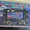
Yes that is a 2019 OG Wii PMS. No, it did not even have the updated 2.0 FW from the late 2019 orders.
First thing first - I ordered myself a PICKIT3 and flashed the updated FW onto the Wii PMS so I can now properly negotiate USB-C PD.

Quick and dirty test to make sure the Wii still booted - great success.

Whilst I was here I also updated BBLoader to RVLoader because we live in a society.
OK.
Lets start the first goal - be easily serviceable.
I will likely be adding and removing components a lot during this build. plastic does not fair well from screws coming in and out.
So - let's add some threaded inserts to all the things.
I modified the top and bottom G-Wii STL in Tinkercard and enlarged all screw posts to be compatible with M2 heatset threaded inserts.
Here's a screenshot of the top as a reference:

Here is the vision come realised:


Tested some board fitment and it's working as well as I'd hoped. No more cracking or stressed screw posts. These puppies will outlast the cheap AliExpress screws threaded into them.
Next on the agenda - Limit the number of wires/conductors that go between the 2 halves
A couple months ago while getting inspiration to resturn to this build, I saw a number of G-Wii's with PCB breakouts for the the buttons and joysticks. Brilliant idea I thought!
I tracked down the original creator and reached out to Pickles/Ethan, but understandably as it had been over 4 years he didn't have any boards left or the CAD files kicking around anymore.
Thankfully, I had spent the past 4 years dabbling in PCB creation making mods for the OG Xbox and a number of home automation ESPHome gadgets - so what would have been unachievable back in 2021 for me, I now felt comfortable attempting to not only re-create but update to suit my goals.
2 months later - I had finished the design of the boards, and sent off for fabrication by the #notsponspor of this post JLCPCB

The button breakouts are fairly self explanatory.
Probably worth noting is the hole in DPAD PCB - this is to fit a 3D printed plug that the DPAD can rotate around so all 4 buttons cannot be pressed at the same time.

The tactmount board has a dual-purpose button to make testing/final build easier.

There are jumpers on the board. If both jumpers bridge 1&2, the 4th button becomes SOURCE so I can switch between Composite and VGA should I need to during troubleshooting (spoiler - I did)
If both jumpers bridge 2&3, the button becomes BT Sync.
The fun one is the large connector board, and the smaller breakout that go on each half of the G-Wii case.
The premise is simple - instead of wiring up all the video/audio/IO from one side to the other, why not use 2 FFC cables to make the solution much cleaner and easier to separate.
I have also added a number of quality-of-life jumpers on the board to assist in troubleshooting.
MODE is a jumper - should allow me to change between composite and VGA without desoldering/resoldering anything
UAMP DP is a jumper - allows me to set DP as either 1.8V or 3.3V to allow either analog or digital audio
J2 on the UAMP is a jumper - for the same reason as above - needed to set audio as analog or digital.
The 2 footprints at the bottom are for the UAMP-2 and GC+ 2.0 - the only new parts I bought for this build.
Main board with all the soldery bits done.

Close up of the fun soldery bits.

Test fit in the case - everything fit first time. I was shocked. This never happens.

Well - almost everything. I went in knowing the standard LED would be 2mm too tall. 2 minutes of sandpapering later and NOW everything fits.

This was the moment I learnt I should add more tolerances between boards. CAD fitment does not always reflect reality.
Thankfully with a specific order of operations it all fits together.

I am aware this image is very much a "now draw the rest of the fucking owl", but we've all seen a trimmed Wii in a G-Wii shell before.
This instead shows off the breakout board, lovingly dubbed "Wii Got Signals".

Having now soldered it all up, there are definately some changes I would make for the next revision of the board - namely where the voltage pads are on the breakout.
It's fine, but there likely better ways, like a JST connector instead of bare pads.
OK back to the top of the case.
I knew the VGA board would interfere with the FFC connectors so I planned to mount the board 2mm above. This proved hard in CAD due to the screen's flex cable so I opted to add them afterwards.
I printed off some spacers and added some more heatset threaded inserts.
I then quickly designed some Jigs to align the VGA board straight, 9mm off the top. I am using the flex cables own resistance to push the board into the jigs
Once in place I added some glue around each spacer to affix it to the connector board.

With the jigs still in place and glue to be cleaned up.

Final result - great success!

I ordered some flex cables from AliExpress but as of yet they have not arrived.
In the interim I cut down an old WiiKey cable I had to 14pin to test composite video signal between the 2 breakout boards
Please ignore placeholder duPont power wires.

Great success - FFC cables are doing the do!

At this stage I could post more - however in doing some testing 2 nights ago to try to figure out why audio wasn't working, the Wii suddenly no longer boots.
I don't know why. The PMS still powers up. It still provides all correct voltages to the board, but the I get nothing more than a blank screen. I have tried on both VGA and composite with no luck.
Further testing last night with my charge reader showed it was pulling 0W.... that's odd.
I desoldered the VSYS wire from the Wii on the off change it was doing something bad. I also removed all but 1 battery.
Testing charge now - I am drawing a stable 9V 500mA 5W of power.
That's better. But in testing, the Wii still doesn't appear to boot.
I have tried direct soldering to the CV via on the Wii and testing on my TV - still nothing.
The only change I made realistically in testing was changing the UAMP DP jumper from 1.8V to 3.3V.
In any scenario I can think of, if I had shorted VSYS or done something dumb on the UAMP - the damage should have been the to the PMS or the UAMP, not the Wii itself?
I am likely going to buy an oscilloscope to check if the Wii is actually turning on or not. My only troubleshooting method right now is "do I see video?" which I admit isn't the greatest metric of success.
So I shall end this post for now - and will post more once I have more.
If you want these breakout boards yourself - you can find them in my GitHub here:
https://github.com/buzzyc/gwii-breakout-boards
Figured at this point I should create a worklog of the progress from the past 3 months of trying to revive a G-Wii project I shelved back in 2021 as it never felt as polished as I'd have liked.
This time around, I went into the project with a number of goals to make the best possible G-Wii I could with a mix of both old and new parts. It has to achieve the following:
- Be easily serviceable
- Re-use parts I already have unless they are too cumbersome to integrate
- Limit the number of wires/conductors that go between the 2 halves
- Avoid soldering directly onto plastic (such as the 3D print button mounts)
Yes that is a 2019 OG Wii PMS. No, it did not even have the updated 2.0 FW from the late 2019 orders.
First thing first - I ordered myself a PICKIT3 and flashed the updated FW onto the Wii PMS so I can now properly negotiate USB-C PD.
Quick and dirty test to make sure the Wii still booted - great success.
Whilst I was here I also updated BBLoader to RVLoader because we live in a society.
OK.
Lets start the first goal - be easily serviceable.
I will likely be adding and removing components a lot during this build. plastic does not fair well from screws coming in and out.
So - let's add some threaded inserts to all the things.
I modified the top and bottom G-Wii STL in Tinkercard and enlarged all screw posts to be compatible with M2 heatset threaded inserts.
Here's a screenshot of the top as a reference:
Here is the vision come realised:
Tested some board fitment and it's working as well as I'd hoped. No more cracking or stressed screw posts. These puppies will outlast the cheap AliExpress screws threaded into them.
Next on the agenda - Limit the number of wires/conductors that go between the 2 halves
A couple months ago while getting inspiration to resturn to this build, I saw a number of G-Wii's with PCB breakouts for the the buttons and joysticks. Brilliant idea I thought!
I tracked down the original creator and reached out to Pickles/Ethan, but understandably as it had been over 4 years he didn't have any boards left or the CAD files kicking around anymore.
Thankfully, I had spent the past 4 years dabbling in PCB creation making mods for the OG Xbox and a number of home automation ESPHome gadgets - so what would have been unachievable back in 2021 for me, I now felt comfortable attempting to not only re-create but update to suit my goals.
2 months later - I had finished the design of the boards, and sent off for fabrication by the #notsponspor of this post JLCPCB
The button breakouts are fairly self explanatory.
Probably worth noting is the hole in DPAD PCB - this is to fit a 3D printed plug that the DPAD can rotate around so all 4 buttons cannot be pressed at the same time.
The tactmount board has a dual-purpose button to make testing/final build easier.
There are jumpers on the board. If both jumpers bridge 1&2, the 4th button becomes SOURCE so I can switch between Composite and VGA should I need to during troubleshooting (spoiler - I did)
If both jumpers bridge 2&3, the button becomes BT Sync.
The fun one is the large connector board, and the smaller breakout that go on each half of the G-Wii case.
The premise is simple - instead of wiring up all the video/audio/IO from one side to the other, why not use 2 FFC cables to make the solution much cleaner and easier to separate.
I have also added a number of quality-of-life jumpers on the board to assist in troubleshooting.
MODE is a jumper - should allow me to change between composite and VGA without desoldering/resoldering anything
UAMP DP is a jumper - allows me to set DP as either 1.8V or 3.3V to allow either analog or digital audio
J2 on the UAMP is a jumper - for the same reason as above - needed to set audio as analog or digital.
The 2 footprints at the bottom are for the UAMP-2 and GC+ 2.0 - the only new parts I bought for this build.
Main board with all the soldery bits done.
Close up of the fun soldery bits.
Test fit in the case - everything fit first time. I was shocked. This never happens.
Well - almost everything. I went in knowing the standard LED would be 2mm too tall. 2 minutes of sandpapering later and NOW everything fits.
This was the moment I learnt I should add more tolerances between boards. CAD fitment does not always reflect reality.
Thankfully with a specific order of operations it all fits together.
I am aware this image is very much a "now draw the rest of the fucking owl", but we've all seen a trimmed Wii in a G-Wii shell before.
This instead shows off the breakout board, lovingly dubbed "Wii Got Signals".
Having now soldered it all up, there are definately some changes I would make for the next revision of the board - namely where the voltage pads are on the breakout.
It's fine, but there likely better ways, like a JST connector instead of bare pads.
OK back to the top of the case.
I knew the VGA board would interfere with the FFC connectors so I planned to mount the board 2mm above. This proved hard in CAD due to the screen's flex cable so I opted to add them afterwards.
I printed off some spacers and added some more heatset threaded inserts.
I then quickly designed some Jigs to align the VGA board straight, 9mm off the top. I am using the flex cables own resistance to push the board into the jigs
Once in place I added some glue around each spacer to affix it to the connector board.
With the jigs still in place and glue to be cleaned up.
Final result - great success!
I ordered some flex cables from AliExpress but as of yet they have not arrived.
In the interim I cut down an old WiiKey cable I had to 14pin to test composite video signal between the 2 breakout boards
Please ignore placeholder duPont power wires.
Great success - FFC cables are doing the do!
At this stage I could post more - however in doing some testing 2 nights ago to try to figure out why audio wasn't working, the Wii suddenly no longer boots.
I don't know why. The PMS still powers up. It still provides all correct voltages to the board, but the I get nothing more than a blank screen. I have tried on both VGA and composite with no luck.
Further testing last night with my charge reader showed it was pulling 0W.... that's odd.
I desoldered the VSYS wire from the Wii on the off change it was doing something bad. I also removed all but 1 battery.
Testing charge now - I am drawing a stable 9V 500mA 5W of power.
That's better. But in testing, the Wii still doesn't appear to boot.
I have tried direct soldering to the CV via on the Wii and testing on my TV - still nothing.
The only change I made realistically in testing was changing the UAMP DP jumper from 1.8V to 3.3V.
In any scenario I can think of, if I had shorted VSYS or done something dumb on the UAMP - the damage should have been the to the PMS or the UAMP, not the Wii itself?
I am likely going to buy an oscilloscope to check if the Wii is actually turning on or not. My only troubleshooting method right now is "do I see video?" which I admit isn't the greatest metric of success.
So I shall end this post for now - and will post more once I have more.
If you want these breakout boards yourself - you can find them in my GitHub here:
https://github.com/buzzyc/gwii-breakout-boards
Attachments
Last edited: