Worklog [2026 Summer contest] GBAWii4 & Wii Pico, a redesigned Wii motherboard in a GBA Cartridge

RoseDagger

.
.
2021 2nd Place Winner
Joined
Jan 15, 2021
Messages
60
Likes
176
Location
Not quite socialist North Europe
Portables
GB Adwiince v2, GB Adwiince v3 Revenge
Heya, I’m back again this year!

I kept thinking about what I should do for this year’s competition…
I have been researching a potential ps3 slim cech2500 portable with quite some potential cutting opportunities, but it is still at least a year away.
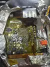
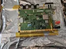
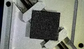
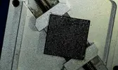
So how could I push past what I tried last year this year? Then it hit me: a redesigned Wii motherboard! If I could transplant the CPU, GPU, RAM and NAND onto a completely redesigned motherboard, then maybe I could make the smallest Wii ever built!

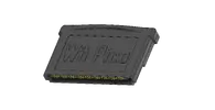
After messing around for a bit, I came to a size of 31x49mm, and checking around, I found a GBA cartridge is 35x57mm, so in theory I could fit the Wii into a GBA cart! And that was way too tempting to not try!

1779226953686.webp


As such my current plan is 3 separate things.
  1. Wii Pico, which is the redesigned Wii, fitted inside a GBA cart
  2. GBAWii4, which is a GBA shaped handheld console similar to my previous ones, but with the twist that the Wii Pico plugs into the GBAWii4, and the GBAWii4 is only a dock. Also, last time I did like 5 pcbs which connected together, this time I’ll make one single PCB instead. I’ll also re-CAD the whole thing as my first attempt at CAD last year was a mess.
  3. Currently unnamed GameCube dock, where you can fit the Wii Pico into. It is similar to the GBAWii4, but shaped like a mini-GameCube, and intended for TV hookup, and to be the smallest Wii ever made. (Or maybe I’ll make it look like a SNES or Famicom as they have cartridge slots? I'll explore the design more as I go.)
1779228252085.webp


Now there are a few issues I've discovered so far:
  1. The Wii Pico has no cooling, I plan to CNC machine the case to act as a heat spreader, while the actual cooling will be in the docks, so I need to make sure the mating of the Pico and the docks are good.
  2. With my current tracing, I’ve focused on minimal footprint and completely discarded any rules on how tight traces can be, or how the wiggles are shaped. So, there is a high risk of noise issues, crosstalk, signal integrity problems, and probably several other things I haven’t thought of yet which might be a headache.
  3. I moved the DQ groups of the RAM around to allow for better wiring, from my research that should be fine. But if it is not, or something is messed up, then the RAM will be all wrong and I won’t know why it is not booting. It could be the RAM, could be the traces, could be something else I forgot or messed up.
  4. With my current plans, I’m going to offload the AVE/GCVideo to the docks and only have the GPU output pins be fanned out, allowing for each dock to handle the video alone, but it makes the Pico less complete in a way.
  5. I want to keep the GBA cart feel and want to keep the 32 pin out connector to be similar. However, the spacing is not a standard size, and the GBA connector expects way more insertion distance than I have space for.
  6. Probably lots of other issues.
1779227458753.webp

1779227536839.webp

1779227592280.webp

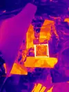
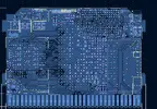
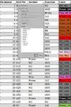
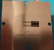
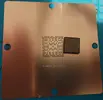
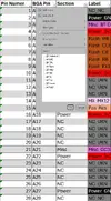
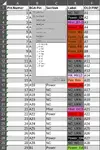
Now to be fair and honest, I started looking into a Wii redesign in January. I used the compendium to trace out all the pins on the GPU, CPU and RAM and added them to an excel spreadsheet with all the pins and their functions. I also made KiCad symbols and did some initial layout mock-ups to see how small I could make it, all before May. It was research and preparation, and I did not actually start building the portable till the 5th of May, but if it is considered to be outside the competition then that’s understandable. I’ll release all the research I did regardless in a future post, likely during the weekend when I have more time. And I’m excited for the project so I will work on it regardless.

Now I’ll leave it there as I don’t want the first post to be too long. I’ll update with a separate update on just the redesign, all the research, excel sheets, KiCad symbols, and schematics and layout mock-ups. And I’ll make an update on the progress towards Pico, the GBA cart CAD, and so on.

Main goals:
  1. Fully redesigned Wii motherboard with transplanted CPU, GPU, RAM and NAND.
  2. Putting the redesigned Wii into a GBA cart.
  3. Create a simple dock to test that the redesign worked.
  4. Create a handheld dock in the shape of a GBA.
Strech goals:
  1. Create a TV dock, which should hopefully be the smallest Wii ever made (so far).
  2. Actually, having something work at competition end for once. XP
Nice to have:
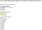
  1. GBAWii4: MX, GCVideo, MelonHD, MIPI display and redesigned driver board.
  2. TV Dock: MX, Bluetooth, AVE/component out, sensor bar plug, 4 GC controller ports.
1779227739232.webp


Wish me luck ^^ Hopefully I can have something really cool and functional at the end!

Also I noticed SimplyStevii is also redesigning the Wii motherboard, but plan to use a Wii mini! I should probably have thought of that, but I’m too deep into using the regular Wii to look back now. Though I’m excited to see how our builds will differ from each other, and if the mini can get even smaller than my solution.
 

Attachments

  • 1779227381638.webp
    1779227381638.webp
    76.1 KB · Views: 3
Wicked ambitious! I hope it all works out for you! Best of luck!
 
This is absolutely nuts!! Looking forward to seeing how far you take this project!
Have you already tried transplanting the chips to get the hang of it? How do you plan on doing that?

I am working on a USB Gameboy Player compatible with the Wii, would be crazy to have your GBA also play actual GBA cartridges lol

Nice GANTT chart
Thank you ^^

I have been working on a PS3 Frankie, and have the pre-heater bed from that, a good hot air station, and a stencil jig for re-balling, so I have tried my hand at it before. And last year I did a redesign of a display driver board which included a mid sized BGA chip.

So I'm mostly going to follow the same procedure as a PS3 Frankie, pre-heater to heat the Wii motherboard up slowly, then the hot air to slowly heat the CPU, GPU and RAM the rest of the way till I can carefully lift them. Then using the jig and stencils for the Wii to re-ball them before I transplant them to the new board.

I'll harvesting the chips next week, and I'll be de-soldering all the passives as I have yet to actually measure them properly. So I'll be making an update on if the harvest was successful.
 
Last edited:
But you will test transplanting them back to the same board for testing? To make sure your process works before testing the redesign and making it simpler to troubleshoot
 
It’s Pico time!

So here is my current progress into redesigning the Wii motherboard.

Most of the work has been looking through the compendium and tracing every pin from the main chips. I’ve used the OMEGA cut as a basis for which traces and passives are important and not, and it has led me to this, a color-coded map of all the BGA pin on the GPU:

1779736435082.webp


And a similar breakdown for the CPU:
1779736507337.webp


The RAM is validated by the publicly available datasheet:
1779736569011.webp
1779736759559.webp

And finally, passives… In order to accurately recreate the motherboard, I need to know what values the various passives and filters have. At the moment I have mapped out the connectivity between each component, but not the component values. I have an SMD tester, which is a pair of tweezers which was supposed to be able to measure the values of all those resistors and capacitors. But it was kinda trash, getting any reading was difficult, and trusting the readings was even worse. And it could not do inductors… As such I plan to use the lab grade LCR (Inductance, Capacitance, Resistance) meter at work to properly measure all the passives properly. I just need to find a way to take some 100 individual, loose, 0402 passives with me to work without losing them or loosing track. XP
1779736917528.webp


Now, my excel sheet also has everything listed as sortable pin lists as well, which makes for easy entry into KiCad:

1779742749219-webp.43080


And with that I’ve created a KiCad schematic with everything wired up:
1779737460080.webp

1779737475362.webp

1779737492281.webp

1779737508095.webp


With Video options:
1779737523738.webp

1779737534887.webp

1779737565315.webp


And with all the schematics set up, I tried doing some layout options, starting with the most extreme version. Putting the RAM and CPU on the back side!

The idea would be to bend a copper plate around to touch both the CPU and GPU to cool them. However, the tracing would be insane and would leave no options for length matching.

1779737842595.webp
1779737909923.webp


The other option that seemed more reasonable was to just flip the RAM, while keeping the CPU and GPU on the front. It would make tracing the CPU way easier, and it would be more similar to some of the discussions around an Ultra cut, I read someone here attempting. However, as I kept fiddling with it, I found it annoying to fit the RAM on the backside as just a direct flip as it would stick out quite a bit.

1779738203184.webp


So, I started looking more at what the pins on the RAM actually was, and saw there were built in options to flip some of the pins of the RAM, along with how the RAM is laid out with 4 DQ groups of 8 bits each. As the RAM is made to be flexible for layout, I decided to try with changing the DQ groups around to see if I could rotate the chip into a better position!
1779738973411.webp


1779738326514.webp

1779738421889.webp
1779738438038.webp


With a layout concept, I started to trace it out. First without any thoughts for any kind of matching, I just wanted to see if it was possible at all. And surprisingly it was! I built upon that, tracing the passives, and adding length matching. I mostly followed gut instinct based on what Nintendo had done on the original Wii, matching the first few rows of the CPU, where I matched them to 11mm. The RAM was way more painful. I managed to match most traces to 8mm, with a few traces being as long as 11.3mm, and the clock lines matched to those longest traces. I also kinda needed to hand wiggle the traces, as KiCad didn’t like the limited space I had available, so there’s an even higher risk due to the uneven trace wiggles.
1779738537120.webp

1779738561635.webp
1779738754730.webp

1779738609993.webp
1779738670881.webp

1779738716260.webp


Finally for the Pico, I also added the power regulators from the ThunderVolt (by YvetalGriffin), so it has built in power. And I added the GBA cartage connector, which is 32 pins, with a pitch of 1.5mm, and decided to break it out as such:

GND x2
VDD x1
Bluetooth x2
USB x2
GC controllers x4
MX x4
I2S audio x4
Video x10
I2C x2
Button x1
1779738832614.webp


As you might have noticed, I decided to not put the AVE or GCVideo on the PICO, and instead I’m outputting the GPU data directly. The main reason is that it allows for flexibility where the dock can decide if it wants the AVE or HDMI. And the second reason is that there is very little space left, and I didn’t feel like adding it in XP
1779739033188.webp

1779739085190.webp
1779739105673.webp
1779739122723.webp
1779739148588.webp
1779739188908.webp
1779739162116.webp

1779739218936.webp


Now to conclude this log, I took up the suggestion to practice on replacing the GPU, CPU and RAM on a functional board before going for my new board. As such, I setup the preheater, added some probes on the top and bottom, and slowly heated the board. Aaaaand I might have overheated the board a little bit… I forgot to double check what my final target temperature was, and when I opened the foil to heat the GPU what I thought was the rest of the way… I discovered that the GPU was already loose… I had overheated the board to the point all the solder was melted… Which is a little bit of an oopsie... I could give lots of excuses for why I fucked up, but the simplest reason was that I didn’t double check what my final temperature values should have been, I was going of gut feelings and my memory from working the PS3s. And I will definitely do better next time.

Worklog entry.webp

IMG_20260523_131322164_HDR.webp

1779739489530-webp.43072

1779739568541-webp.43073
1779739635937.webp

I should have realized something was wrong as the delta between the top and bottom probe increased from 15C to 70C... And in general I should have been thinking a lot more critically through the whole process... There was so many opportunities to catch that I was messing up badly, had I just stopped to think...

img_20260523_211032025_hdr-webp.43075

(Note to self, PCBs fully de-laminate at 300C)


Ignoring my previous failure, I used the likely overcooked GPU to start practicing re-balling. I had bought a set of stencils which should have included the Wii GPU old, Wii GPU new, Wii CPU old, and Wii CPU new. However, checking the stencils, it seems they forgot to include the new CPU stencil…
screenshot-2026-05-25-211947-webp.43076

cpu-stencil-webp.43077


I also had a set of stencils for different DDR ram modules and found that the DDR3/XBOX CACHE matches the footprint of the Wii RAM.

ram-stencil-webp.43078


I’m getting a set of universal stencils and plan to try to modify those to fit the Wii CPU, as it is just a simple grid.

I have also started practicing re-balling the GPU, and while I had managed to do the PS3 RSX quite nicely, I’m struggling a bit with the Wii. It does not feel like the balls wants to go into their pins properly. With the PS3 RSX it felt like there were divots that the balls actually fit into, while the Wii GPU is completely flat, and the balls likes to wander… But I’ll keep practicing and waiting on a new Wii that I can try to transplant the GPU into.
Attempt 2: Prepping the surface
1779743062493-webp.43082

Stencil with balls
1779743113282.webp

Adjusting the balls before heat
screenshot-2026-05-25-220550-webp.43084

After applying heat...
screenshot-2026-05-25-220856-webp.43085


Attempt 3: Before heat
screenshot-2026-05-25-221101-webp.43086

Attempt 3: After heat
1779744719769.webp

Going to need quite a bit more practice before I get it right.
And I think that is where I will leave the worklog for now. I’ll be updating the Excel document as I add in the passives. And I'll upload the KiCad files in a future post.
 

Attachments

  • 1779739568541.webp
    1779739568541.webp
    54.4 KB · Views: 1
  • 1779739489530.webp
    1779739489530.webp
    504.9 KB · Views: 6
  • 1779739055082.webp
    1779739055082.webp
    130.3 KB · Views: 1
  • IMG_20260523_211032025_HDR.webp
    IMG_20260523_211032025_HDR.webp
    897.1 KB · Views: 1
  • Screenshot 2026-05-25 211947.webp
    Screenshot 2026-05-25 211947.webp
    60.4 KB · Views: 4
  • IMG_20260523_131322164_HDR.webp
    IMG_20260523_131322164_HDR.webp
    794.7 KB · Views: 1
  • Screenshot 2026-05-25 220856.webp
    Screenshot 2026-05-25 220856.webp
    136.3 KB · Views: 1
  • Screenshot 2026-05-25 220550.webp
    Screenshot 2026-05-25 220550.webp
    526.5 KB · Views: 1
  • 1779743062493.webp
    1779743062493.webp
    490.2 KB · Views: 2
  • WiiPinout V1.0.xlsx
    WiiPinout V1.0.xlsx
    8.1 MB · Views: 4
  • 1779742749219.webp
    1779742749219.webp
    69.2 KB · Views: 2
  • RAM Stencil.webp
    RAM Stencil.webp
    64.7 KB · Views: 2
  • Cpu Stencil.webp
    Cpu Stencil.webp
    93.1 KB · Views: 2
  • 1779737030867.webp
    1779737030867.webp
    54.3 KB · Views: 2
  • 1779736986765.webp
    1779736986765.webp
    74.4 KB · Views: 2
Damnn this thing is looking crispy (no pun intended lol)
 
And finally, passives… In order to accurately recreate the motherboard, I need to know what values the various passives and filters have. At the moment I have mapped out the connectivity between each component, but not the component values. I have an SMD tester, which is a pair of tweezers which was supposed to be able to measure the values of all those resistors and capacitors. But it was kinda trash, getting any reading was difficult, and trusting the readings was even worse. And it could not do inductors… As such I plan to use the lab grade LCR (Inductance, Capacitance, Resistance) meter at work to properly measure all the passives properly. I just need to find a way to take some 100 individual, loose, 0402 passives with me to work without losing them or loosing track. XP

JacksonS measured pretty much all of the passives on the Wii years ago, Shank's super thread should help you identify most of them: https://bitbuilt.net/forums/threads/shanks-wii-super-thread.66/

Best of luck!
 
If you want to improve the viability of the BGA transplant, the last successful attempt at a mobo recreation dried the board at ~100c for 8 hours to get all the trapped moisture out of the dies before extraction and transplanting. Ideally you'd do both right after the drying before moisture can get back into the dies
 
JacksonS measured pretty much all of the passives on the Wii years ago, Shank's super thread should help you identify most of them: https://bitbuilt.net/forums/threads/shanks-wii-super-thread.66/

Best of luck!
Thank you ^^ That saved me a lot of work!
Now I just need to measure the filters and the feed-through caps, instead of everything.
Also there were a lot more variety than I expected, I had assumed most of the decoupling caps would have been the standard 100n, but there's a lot of 2.2n and 10n in there as well.

1779778675555.webp


If you want to improve the viability of the BGA transplant, the last successful attempt at a mobo recreation dried the board at ~100c for 8 hours to get all the trapped moisture out of the dies before extraction and transplanting. Ideally you'd do both right after the drying before moisture can get back into the dies
Yeah, I tried to dry it for 2h on 90C, 1h on 100C and 1h on 110C. I should have been more patient and dried it for longer to get the moisture out. And avoided going as high on the temperature as I did.
By the way has there been other successful Wii mobo recreations? I found this thread 2018 with ruumoo and Aurelio talking about Wii recreations, but I've not seen any recent? Unless I just missed it in my search?
 
Thank you ^^ That saved me a lot of work!
Now I just need to measure the filters and the feed-through caps, instead of everything.
Also there were a lot more variety than I expected, I had assumed most of the decoupling caps would have been the standard 100n, but there's a lot of 2.2n and 10n in there as well.

View attachment 43096


Yeah, I tried to dry it for 2h on 90C, 1h on 100C and 1h on 110C. I should have been more patient and dried it for longer to get the moisture out. And avoided going as high on the temperature as I did.
By the way has there been other successful Wii mobo recreations? I found this thread 2018 with ruumoo and Aurelio talking about Wii recreations, but I've not seen any recent? Unless I just missed it in my search?
Holy shit I love this!
B_rob successfully recreated and got one to work. Also Funnyplaying did a while ago.

Those caps you circled are 1uF X2Y caps. The filters are ~150mOhm ferrite beads
 
Also worth mentioning that while we don't know Funnyplaying's success/failure rate, B_rob took his time to triple check everything and got a working transplant first try!

The Wii does use high speed logic so you will have to finagle some trace impedance matching for best results, but if you're careful in your measurement taking and planning, no reason why you can't do the same! You're free to consult with people who have made/attempted transplant boards in the past, so I say ask all the questions and take advantage of their firsthand experience to lessen your list of possible mistakes.
 
Feel free to join the Discord, lots of good info shared there! B_rob exclusively posts on the Discord server and his insights could be helpful for your project
 
From the moment I saw yveltal's remake of the Wii motherboard and also B_robs work I wondered if it would be possible to redesign the board to be tiny. And, you crazy son of a bitch, you're doing it! I will be following this with much excitement.
 
Time for update 3!

I had planned for this one to be focused on the CAD process… However, with B_rob1 releasing his schematics for the Wee Wii PCB recreation, I ended up double checking my pinout first. And good thing I did as I found a few critical issues I had missed! Also, it is really epic seeing B_Rob having a functional Mobo reconstruction! I didn’t know a recreation was already in the works when I initially started planning my reconstruction, but it gives my crazy attempt a way better chance of perhaps maybe hopefully working.

As for the issues, starting with the minor ones: I had labelled some pins as Not Connected/Unknown, but they were supposed to be ground. They would likely not have been a real issue.

For the major issues:
  • I had a Ground pin labelled as 1.8V, so it would have been a short! I had it labelled correctly in the compendium, do I must just have slipped up between the two slightly different greens used in the compendium for ground and 1.8V.
  • On the RAM I had swapped a data pin and a ground pin. I should have caught that as it broke the symmetry. And I would likely have seen it on a recheck.
  • U10 were one pin off, I had followed the wrong trace. I’m not sure if I would have spotted that.
So, 4 wrong pins out of 1205 total pins. But any one of those slip ups would have caused it to not boot…

Plus 3 missing ground pins which were unconnected.
Left is updated/ correct. Right is old/wrong
1780082864279.webp

1780082828505.webp

1780082981416.webp
I also used Rob’s schematic to properly label the CPU pins, and label the unused Not Connect pins, like the disk drive, SD card, GC Card. Which makes it easier to follow what everything does.

1780082361630.webp
1780092551513.webp

1780082519026.webp

1780092458237.webp

I also used the values in Shanks guide with data from JacksonS to fill in the passives and then validated it against Rob’s schematic.

1780083618092.webp

1780083773917.webp


So, with that, my schematic and excel sheet should be correct, based on that Rob’s schematic worked.
Now, to the layout. With the passives characterized, I moved some of them around to better align with the stock Wii. However, with the RAM and NAND being directly under the GPU, there are several passives I can’t place where they should be.

My layout on the left, Rob on the right. The NAND is in the way of 3.3V caps, so they have been shifted.
1780083910095.webp


My layout on the left, Rob on the right. The RAM is in the way of a lot of 1.8V passives, and the clock crystal, so they have been shifted.
1780083975222.webp


Another question was in how much I should care about length matching and impedance matching. I knew on one level that with the speeds we are talking about, I actually had quite a bit of leeway in the trace length mismatch. However, I got paranoid and tried to length match everything as much as I could.

Now that I have Rob’s schematic and can actually see the trace length, which has been validated to work… And I realize I was kinda dumb and spent way too much time on this. The trace length there varies with more than the total length of my longest trace. All the traces could have been the shortest path, and I would still have had less variance than the stock Wii… And apparently the CPU traces can have as much as 3 inches, or 76mm mismatch according the PPC750 datasheet, according to YvetalGriffin… So yeah, I was optimizing for nothing… Though with how much work I put into it, I’m reluctant to go back to shortest path… Even though it might actually be better for signal integrity to not do all those tight compact wiggles…

Stock Wii, with a 15mm skew difference
1780084045621.webp
1780084086574.webp

My longest trace is 11.3mm...
1780084923101.webp


I also started looking into impedance matching, using the calculator in KiCad and JLCPCB to calculate the impedance of my traces. With my traces being limited to 0.1mm due to space, I was playing with copper weight to see how the impedance would change. If I went for 1oz copper weight, on a 6-layer board, with a total thickness of 0.8mm I would get an impedance of ~65 Ohm, but, if I went for 2oz copper then the impedance would drop to ~55 Ohm. And was planning on trying to figure out if there was a specific impedance I should be matching… So, I asked Rob, but apparently, he didn’t really do impedance matching on his board… And checking his traces, they are also 0.1mm, and he used the standard process which is 1oz… So, it seems I was getting lost in details which didn’t really matter.

CPU impedance on the left, RAM on the right.
1 OZ copper weight
1780084824447.webp
1780084401675.webp

2 OZ copper
1780084501982.webp
1780084540729.webp


Now on to what I had planned for this update to be. CAD!

So, the plan is to CNC the GBA Cartridge out of aluminium, and have it act as a heat spreader. Then the dock will be the one responsible for interfacing with it and actually cooling it.

I used Fusion to model the GBA Cart and imported the KiCad PCB in to try and make it fit. The CPU and GPU would face the backside, as it would be the flattest, while the front would have the sticker relief and Wii Pico CNCed in.
1780086437829.webp
1780086471887.webp

1780086564793.webp
1780086590078.webp

1780086656004.webp


The plan was to push the PCB as far into the front as possible to make space for the connector, and that there would be a thermal pad between the IHS and the back casing. I found I could use the original connector if I trimmed it down a bit. (Though I did extend the cart and PCB a bit to make the pins engage, so the cart is 37mm tall instead of 35mm)
Stock GBA cartridge connector on the left. Trimmed connector on the right, showing the pin engagement.
1780086757340.webp
1780086813105.webp

The pin engagement is very low, even with the cart extended by 2mm. It would mostly only engaging on the castellated edges.
1780088692052.webp
1780088798995.webp
IMG_20260529_214804736_HDR.webp

1780088756102.webp


I 3D printed the design to test it, but I didn’t really like it. With how the connector is shaped it would push the dock PCB towards the front, while the cooling would be on the back, and it would make it thicker than I wanted. So, I started looking at if I could push the Pico PCB towards the back and fit the connector on the other side pointing down. I found this thread by Ekterm on delidding the Wii, which would give me more clearance. Following the guide, I delidded the overcooked CPU and GPU, to measure them, and to really see how dead they really were.
(GPU is very very very dead. lots of popcorning/delamination.)
1780089088904.webp


After measuring, remodeling, and putting the new Pico PCB model it into Fusion, I found that maybe, just maybe, I could fit it. A bit of inset to the minimum wall thickness JLC allows, using thermal paste instead of thermal pads, and insetting the other side a bit… Then maybe.

1780089662013.webp

There is more pin engagement, but also a tighter squeeze.
1780089743634.webp


I did a test print, and it does fit with some convincing. Though I might have to sand the top of the connector down a bit, so I don’t bow the PCB. I also need to figure out how to secure the PCB better, as it is now, I’m afraid the connector will push the PCB up. And it does not really stay still in the new position.

1780089201251.webp
1780089377474.webp
1780089457419.webp

1780089531767.webp


I also started on a quick test dock. It’s primarily just to test if the Mobo reconstruction works. It uses the AVE, and supplies power, and has a GC port, and USB port. It's a very quick mockup, just so I have something to test with.

1780089954747.webp
1780090046659.webp
1780090081128.webp


I’m planning on sending the test dock (once it's done) and the Pico PCB off for manufacturing sooner rather than later, so that I can test if it works, or debug why it does not work. All before I start on making proper docks. And before I send the case to be CNCed.


Now the worklog has caught up to all the work done in May, and I'm back at work next week, so might be a bit longer before the next proper update. But we will see if anything interesting happens sooner that is worthy of an update.

Though I did manage to do quite a lot! I have a full schematic for the Wii, verified against Rob’s working schematic. A super dense layout fully traced out, and overly length matched. A CAD of the cartridge, which only needs some final adjustments. A test dock to check it this crazy concept will actually work. And it is still only May!

And I want to give a massive kudos to B_rob1 for making the Wee Wii recreation schematic open source! It helped validate my design, and I plan to do the same if the Wii Pico works, or even if it does not work XP
 
You said you were going to use the power regs from a thundervolt, does this mean it's going to undervolted? Also, are you going to use a Hollywood 2 GPU like the kawaii?
 
You said you were going to use the power regs from a thundervolt, does this mean it's going to undervolted? Also, are you going to use a Hollywood 2 GPU like the kawaii?

Ah yes, I used the ThunderVolt regs, as I had already used them in my ThunderKill last year, so I were familiar with them. And they are very small and compact.
How much of an undervolt I would get is a lower priority as the focus is on compactness and getting it to boot.
As for Hollywood-2, I had been so focused on the regular Wii, that I forgot the Wii mini existed, so I only have Hollywood-1s. If the GPU in the new Wii I just got also dies, I might start looking at sourcing Wii minis to get a HW2.

Think I forgot to include the ThunderVolt regs in my previous updates
1780209771374.webp

Here are them highlighted, placed around everything else, close to their power planes
1780209524659.webp


1780209721342.webp


And newest 3D render as I forgot to include that in the last update.
1780210035862.webp

1780210076832.webp
 
Back
Top