
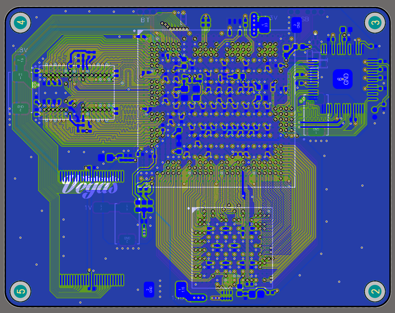
After months and months of procrastination, I've finally begun assembling a prototype of my Wii motherboard redesign, which I'm calling Vegas. The name is an homage to Nintendo's naming scheme for the Wii's chipset (Broadway and Hollywood, both famous hubs of entertainment in the US). I designed the proto board in Altium, referencing both the compendium and additional mobo scans I took. While I tried to replicate the Wii's stackup as closely as possible, I couldn't get the GDDR3 impedances to where I would've liked. Worst case, I can try tweaking the GDDR3's ZQ termination resistor.
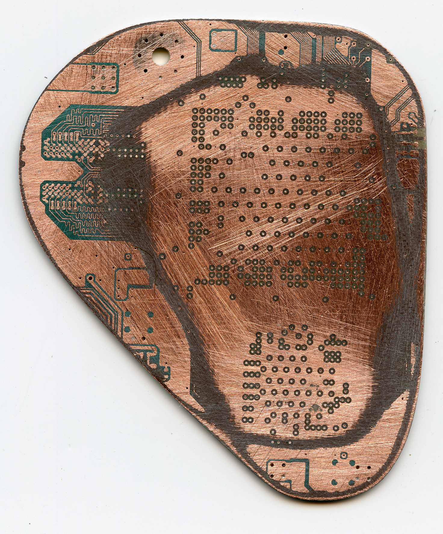
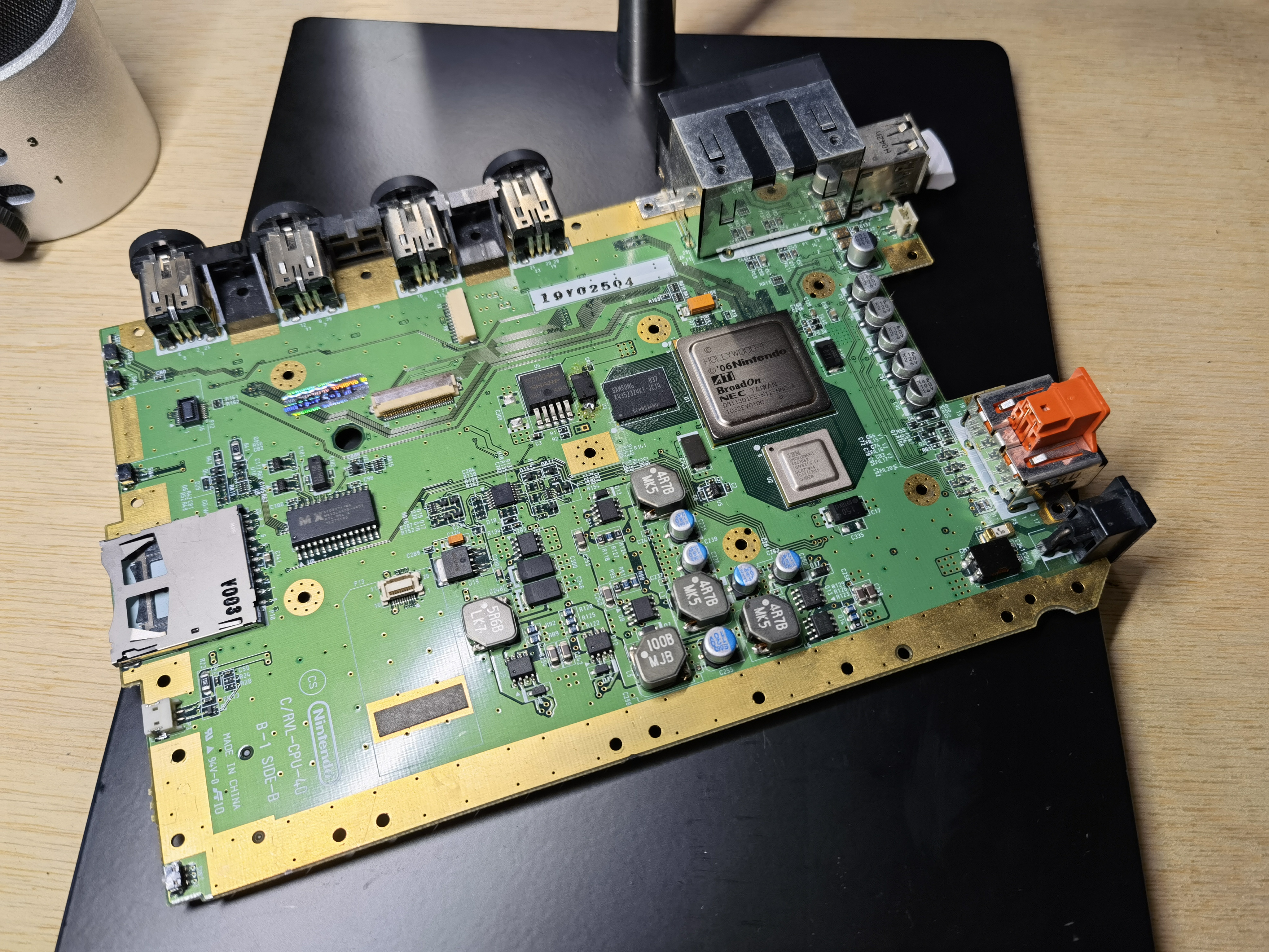
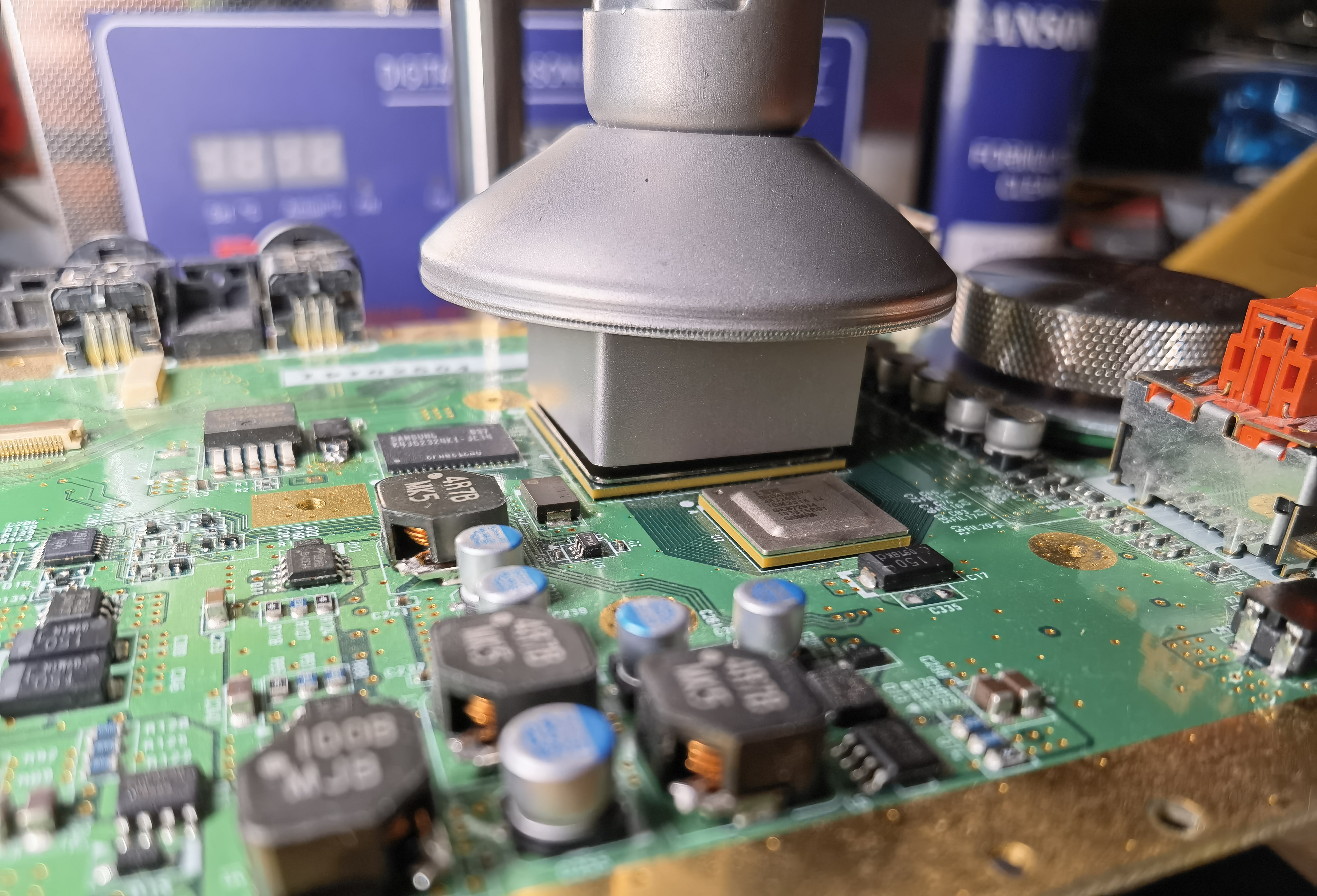
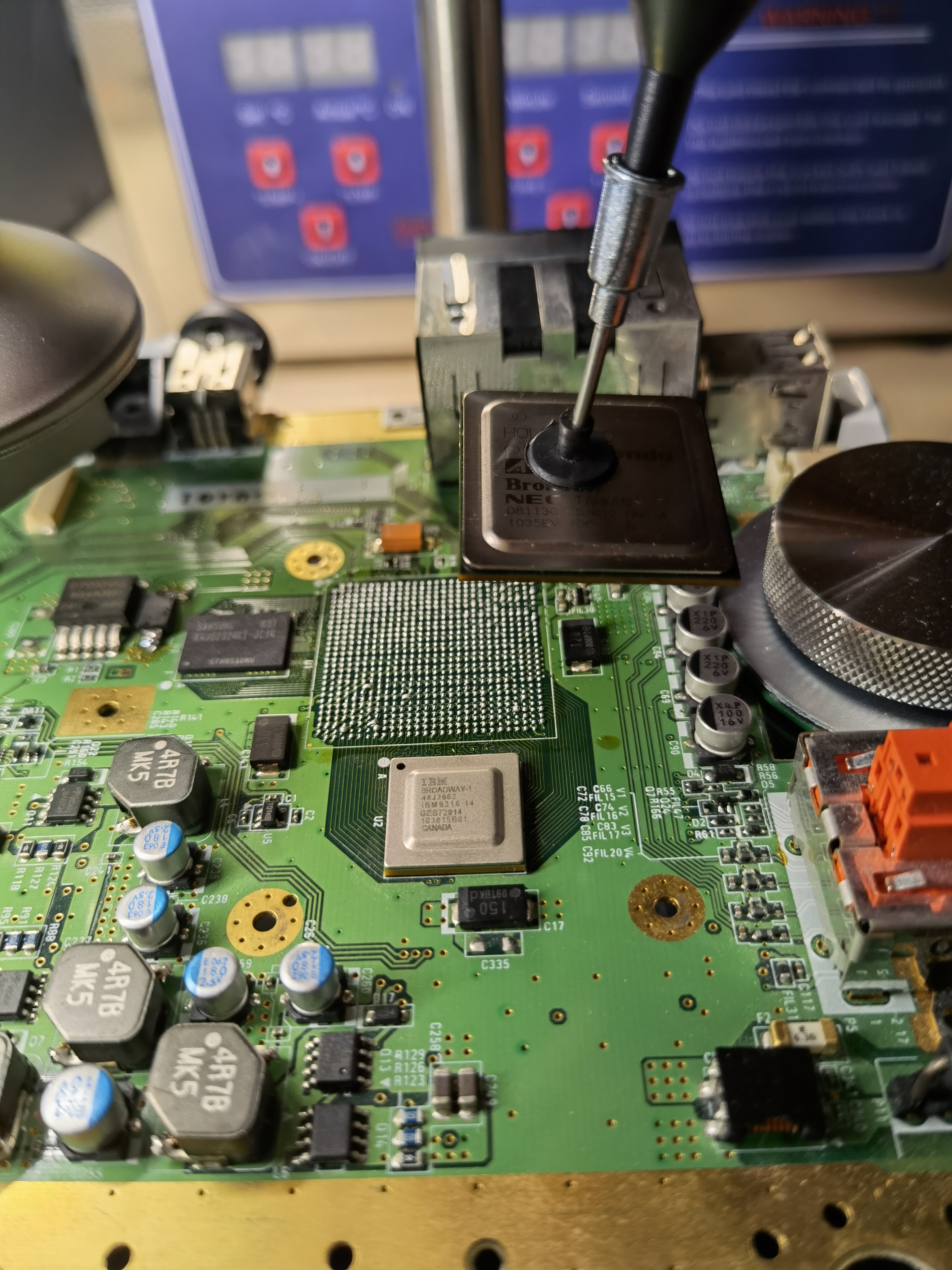
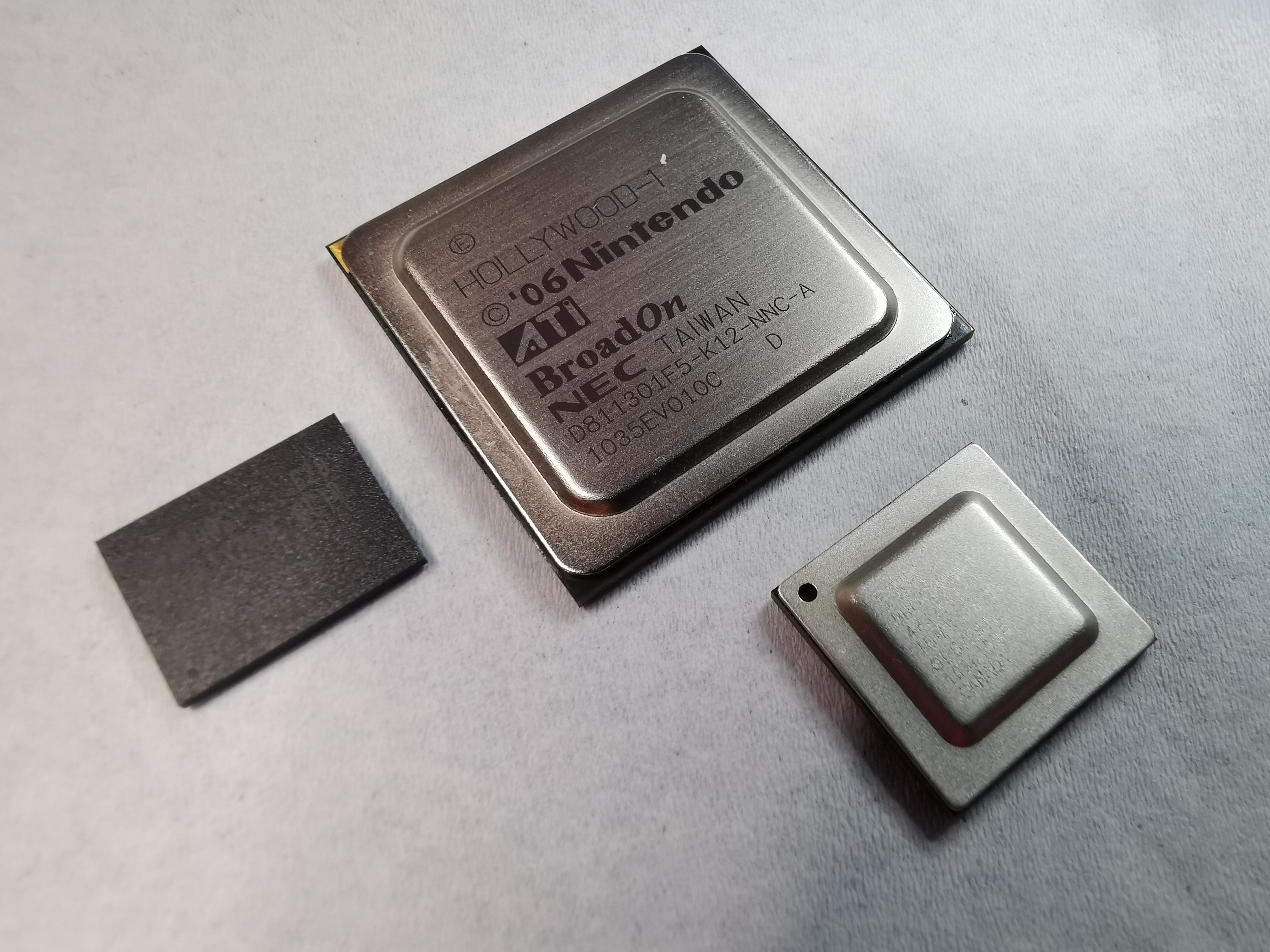
This ready and willing RVL-CPU-40 was the donor motherboard. The first step was to desolder the Hollywood and Broadway. I bought some neat BGA hot air nozzles that match the size of the Wii GPU and CPU to make things easier. (Flux added around perimeter of Hollywood after pic was taken)
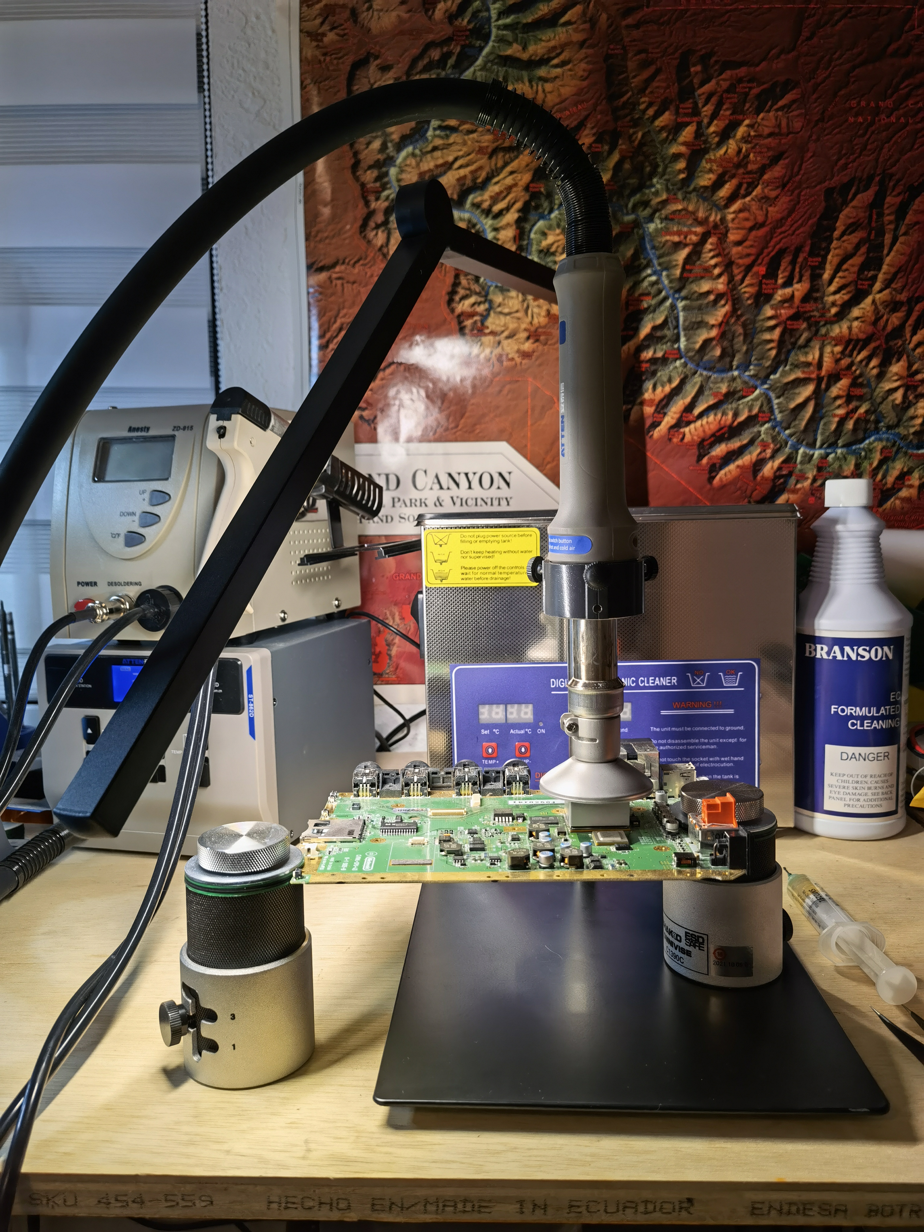
I'm pretty happy with my workbench setup for this process. The Omnivises, hot air stand, and vac pick-up tool really streamline things.
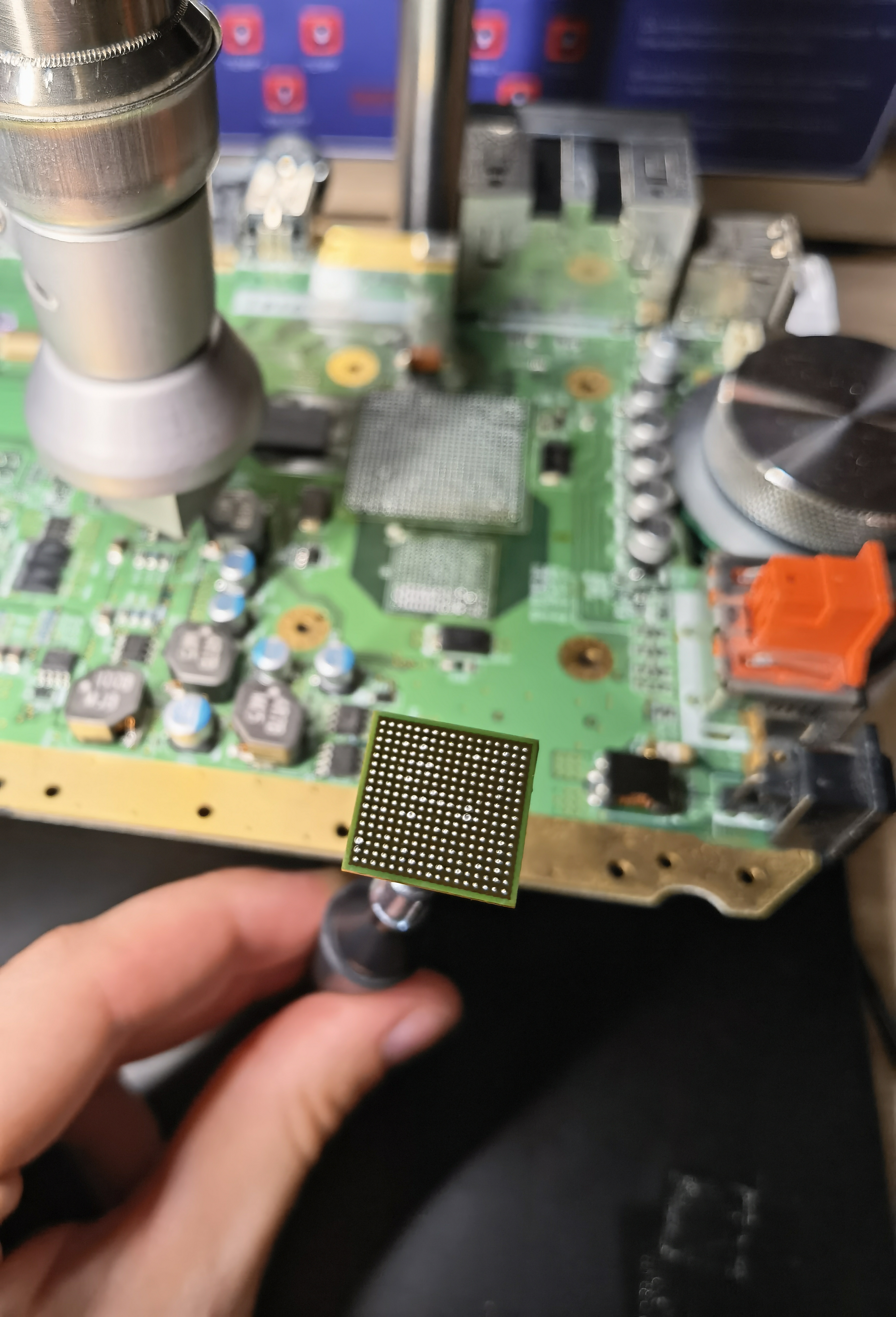
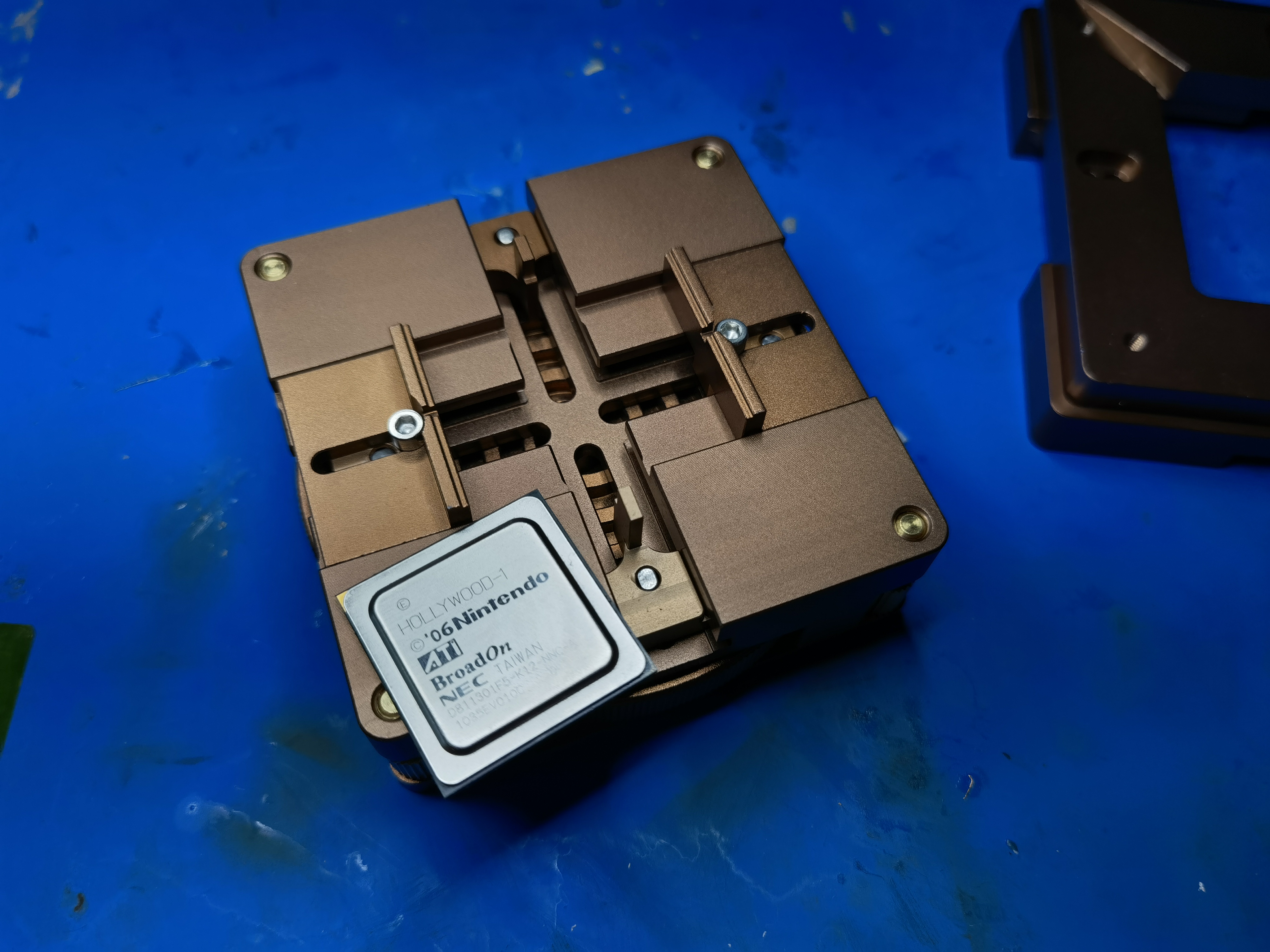
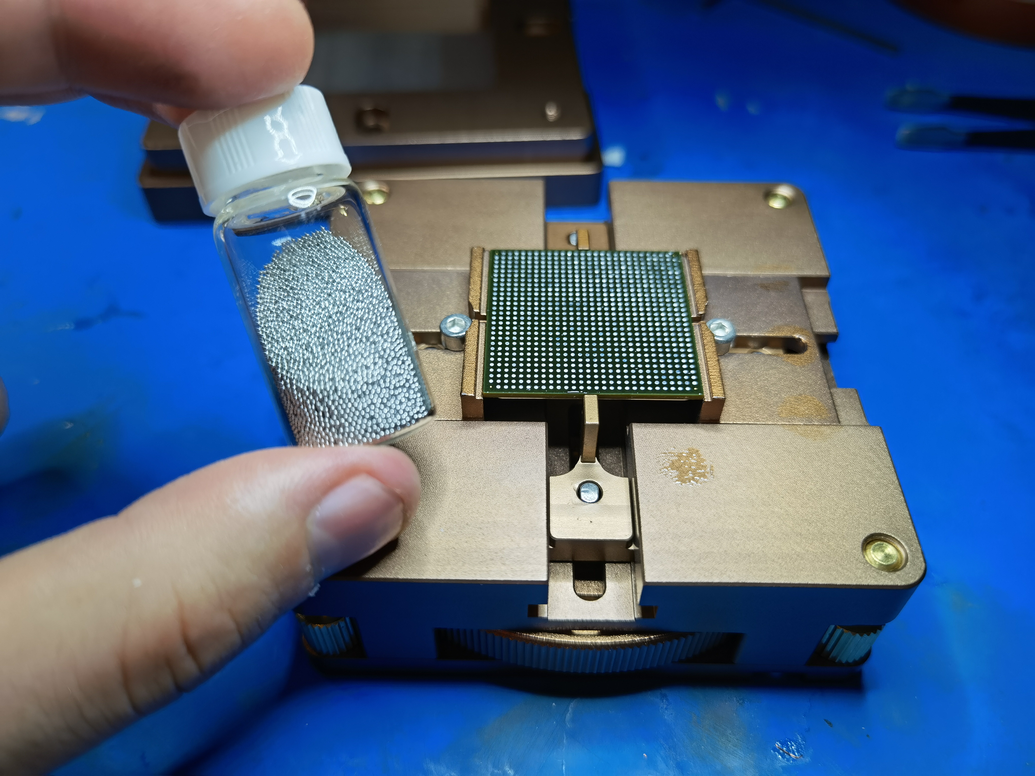
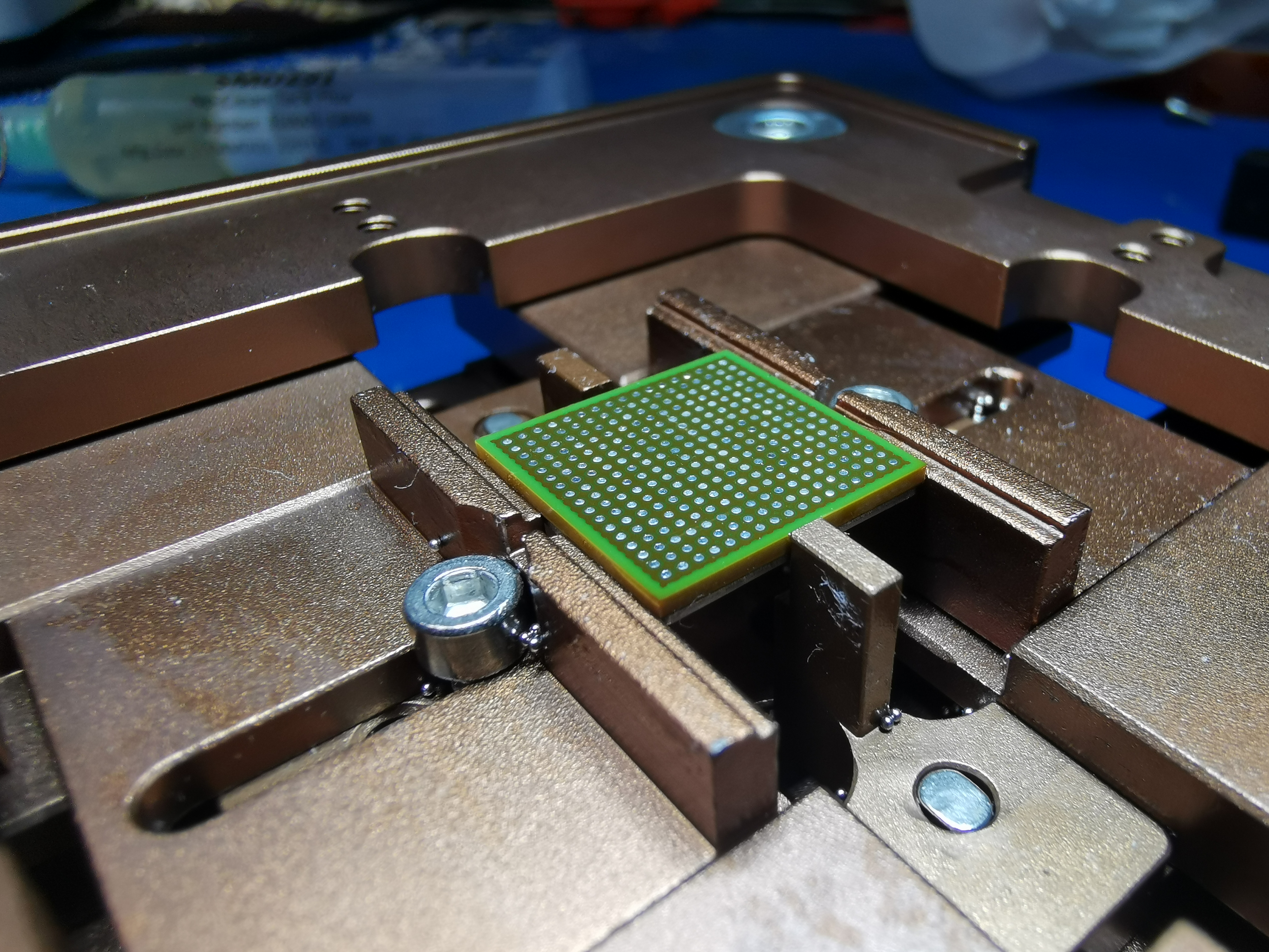
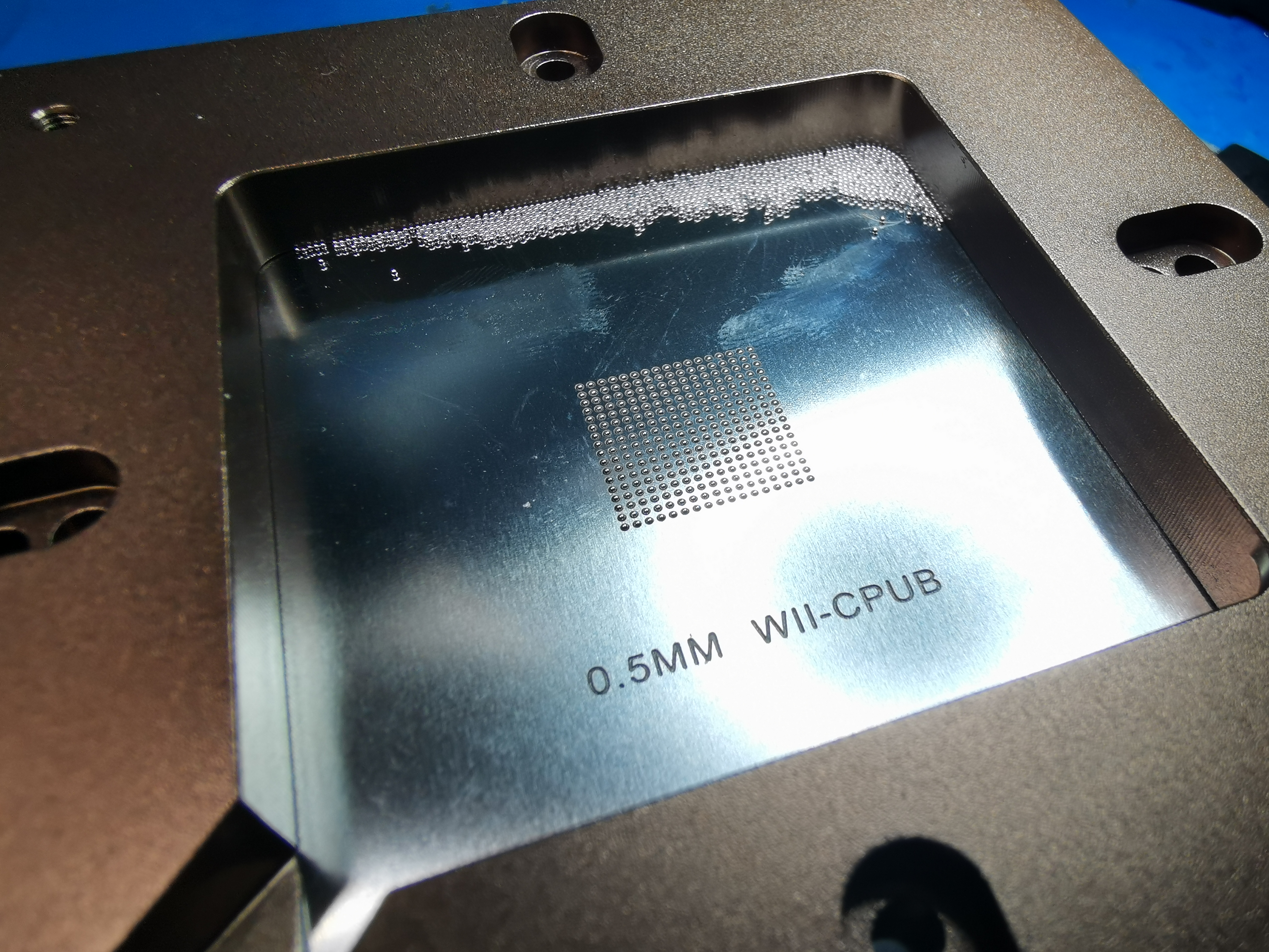
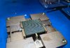
Next is reballing. The overall process is as follows: clean BGA pads with 63/37 solder, flux, and solder wick; apply thin layer of tacky flux to the bare chip; use reball jig and stencil to apply solder balls; reflow under gentle hot air. The magnetic jig I'm using is pretty good, but it's still challenging to get the chip level and flush with the underside of the stencil. Speaking of stencils, I got an assortment of video game console stencils that included Wii-specific ones. No fooling around with universal stencils here.
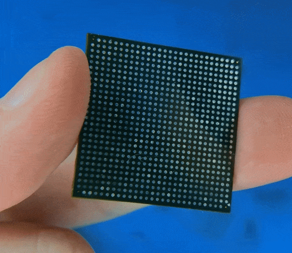
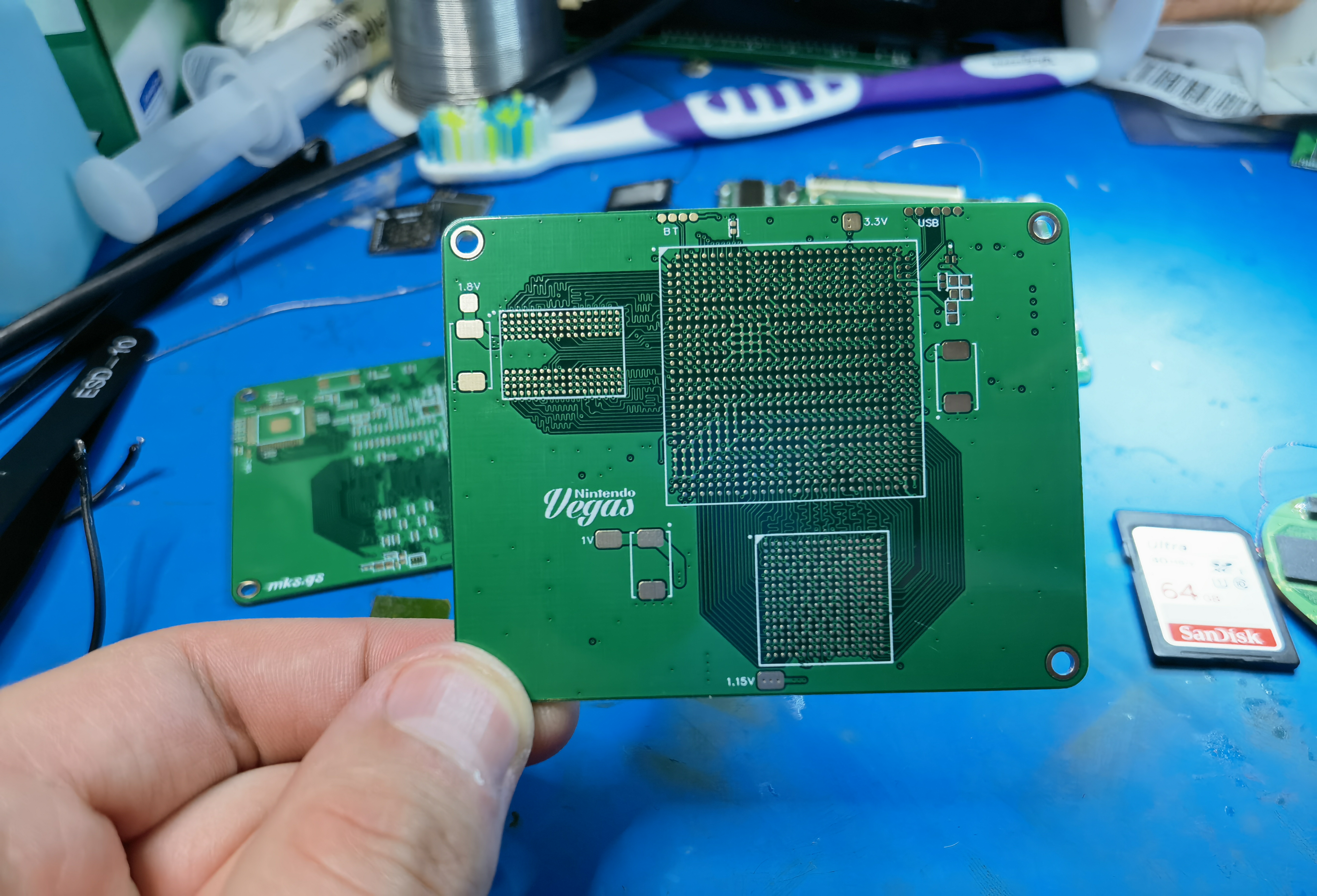
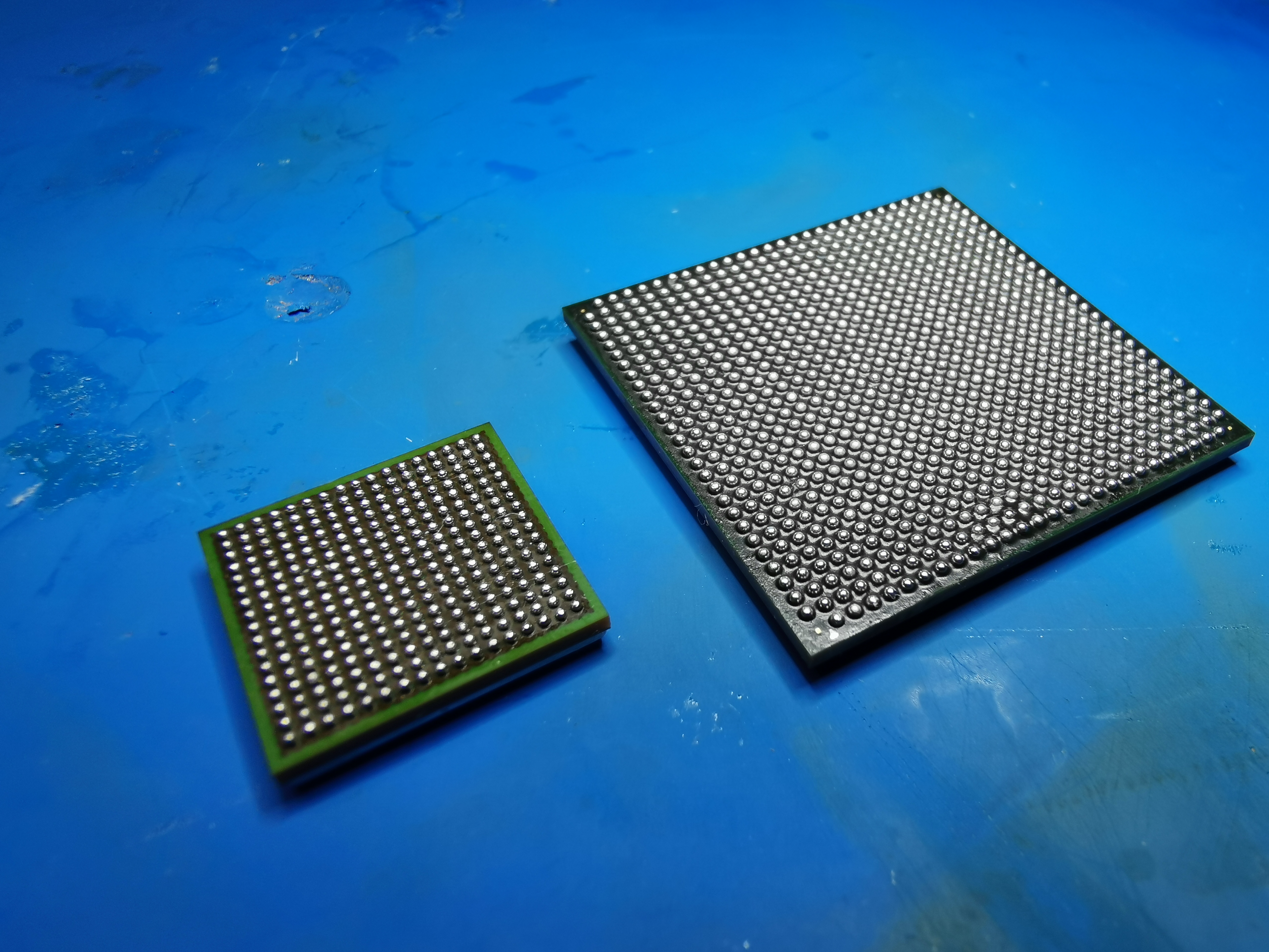
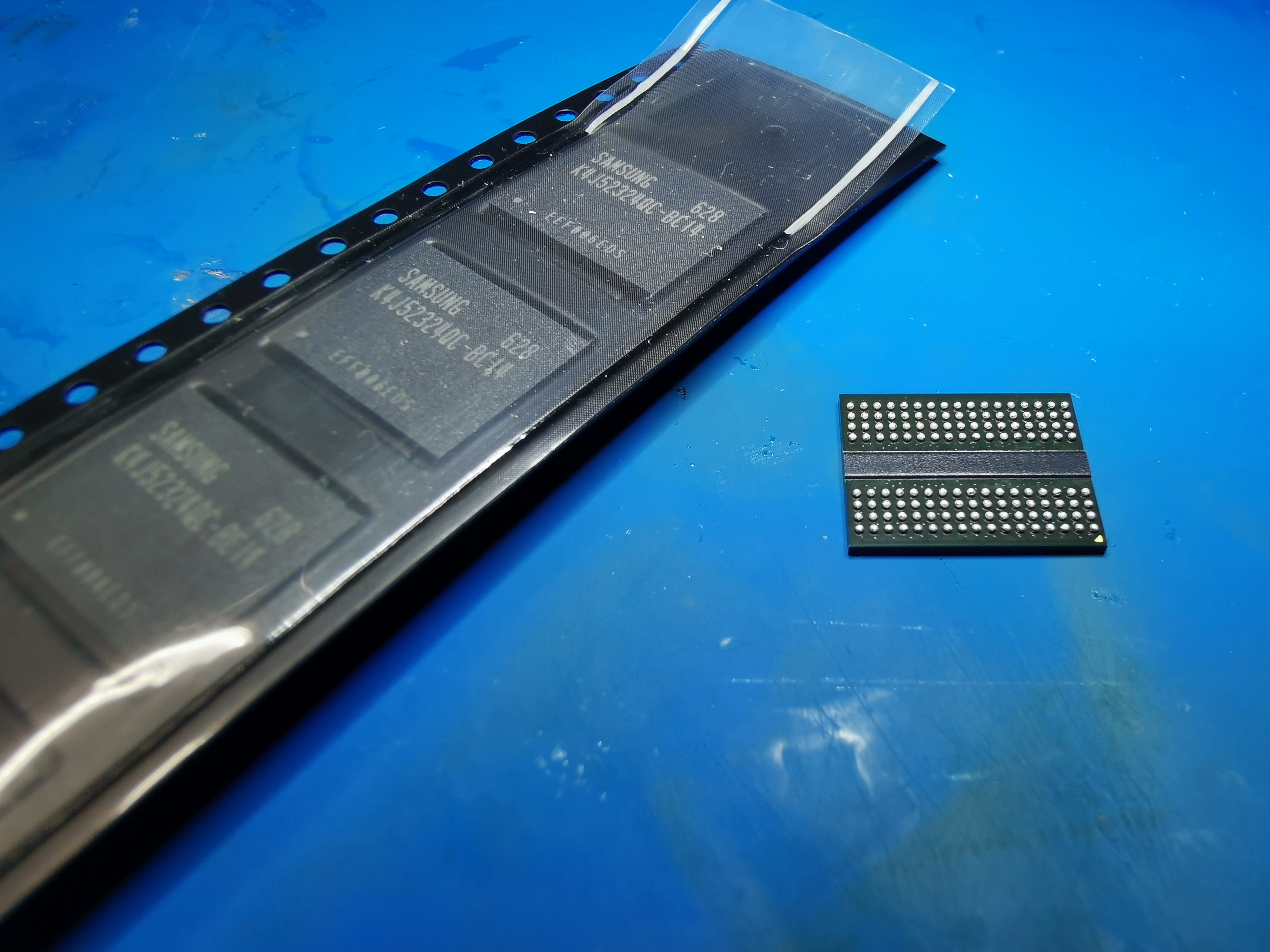
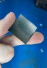
After a couple tries, I mostly got the hang of the process and had a sexy reballed Wii chipset on my hands (and solder balls ALL over my workbench). Luckily, I bought fresh GDDR3 for this project, so I didn't have to desolder and reball the original RAM.
Hopefully all these image embeds don't break... Next post will cover assembling the PCB!
This ready and willing RVL-CPU-40 was the donor motherboard. The first step was to desolder the Hollywood and Broadway. I bought some neat BGA hot air nozzles that match the size of the Wii GPU and CPU to make things easier. (Flux added around perimeter of Hollywood after pic was taken)
I'm pretty happy with my workbench setup for this process. The Omnivises, hot air stand, and vac pick-up tool really streamline things.
Next is reballing. The overall process is as follows: clean BGA pads with 63/37 solder, flux, and solder wick; apply thin layer of tacky flux to the bare chip; use reball jig and stencil to apply solder balls; reflow under gentle hot air. The magnetic jig I'm using is pretty good, but it's still challenging to get the chip level and flush with the underside of the stencil. Speaking of stencils, I got an assortment of video game console stencils that included Wii-specific ones. No fooling around with universal stencils here.
After a couple tries, I mostly got the hang of the process and had a sexy reballed Wii chipset on my hands (and solder balls ALL over my workbench). Luckily, I bought fresh GDDR3 for this project, so I didn't have to desolder and reball the original RAM.
Hopefully all these image embeds don't break... Next post will cover assembling the PCB!
Attachments
-
 3.6 MB Views: 258
 -
 2.9 MB Views: 264
 -
 5.1 MB Views: 261
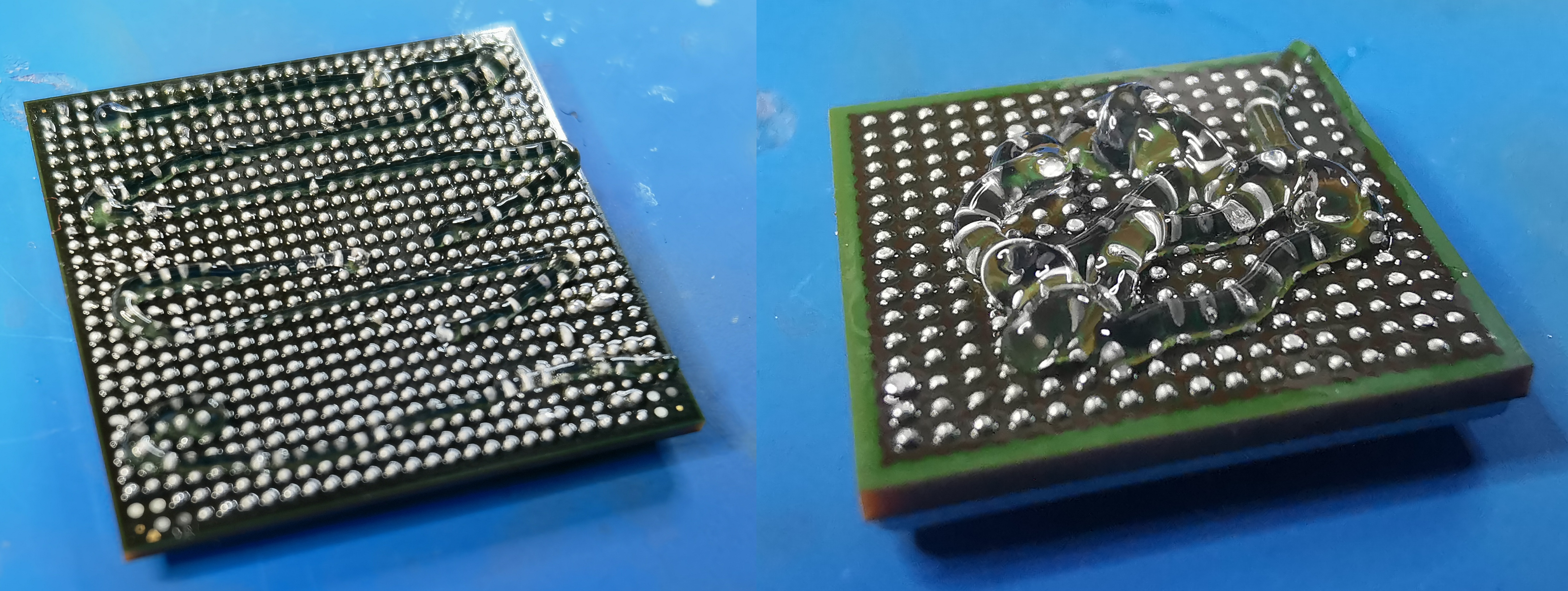
 I reflowed the Hollywood a few times with copious amounts of flux and jiggled it around, but it didn't change anything. Having already taken some glamour shots of the sexy assembled PCB, I desoldered the Hollywood and the short between 3.3V and 1V went away. There must have been some seriously major solder blobbing going on under the BGA for 3.3v and 1v to be shorted together...
")