
Wundervolt (/vʊndɐvo:lt/)
While waiting for my Short Stack boards to arrive, I’ve been working on the idea of building a teeny tiny power supply board with software programmable voltage rails to allow for software Wii undervolting.
Thus wundervolt (pronounced /vʊndɐvo:lt/) was born.
Before I dive into it, wanted to first give a big shout out to Wesk for pioneering and evangelizing Wii undervolting!
Features
This project is initially focused on non-portable builds and “test bench” builds, with the following deliverables:
Part selection
Voltage regulator
There are some really cool multi-output, programmable DC-DC converter ICs on the market, I made a quick summary of some candidates here.
For my first revision, I decided to go with the LP8758-E0 from TI because of how absolutely tiny it is (2.9 x 2.15mm!). This has 4 buck regulators, with up to 4A output per rail, and each rail has programmable voltages so it is ideal for my requirements. The main downside of this chip is that is is expensive at $5.83 per unit!
This chip also has some really cool features that will be helpful for undervolt testing, mainly a load current monitor feature that allows you to measure and read the load on each voltage rail over I2C.
Microcontroller
The regulator chip does not have any non-volatile memory, so we’ll need an external microcontroller to handle things like configuring voltages, persisting voltages, and setting current limits. Having an on-board MCU allows us to add additional features like button press handling (and debouncing) for turning on and off the rails, long-press detection to clear the internal memory and enter “failsafe” mode. It also allows for other future features like powering on when we detect the “power pulse” from the Wii bluetooth module, or controlling addressable LEDs.
I’m choosing the ATTiny1616 MCU for a few reasons
I2C level shifter
If we want to talk to external “host” devices, we need to be able to speak their language. Luckily the Wii has an I2C bus which we can access through homebrew. The Wii I2C bus operates at 1.8V, but I’m planning on operating the regulator IC and MCU at 5V so we need a way to adjust voltages for I2C.
The TXS0102 chip from TI is a cheap, simple level shifter IC for open-drain applications (like I2C) which is also available in a tiny QFN package.
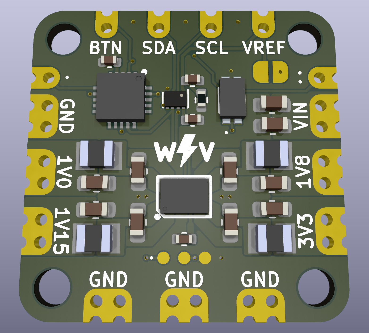
The board
I’ve managed to fit all these components on a 20x20mm PCB. This is my first 4-layer PCB design, and my first time working with BGA chips. Huge thank you to Y2K, CrazyGadget, and YvetalGriffin for their feedback during the past few days as I worked on the board design.
Since this board has a 0.4mm pitch BGA chip on it, it requires precision vias (0.2mm hole, 0.3mm pad) to be placed on the BGA pads, and therefore to use a process called VIPPO (via in pad, plated over). The precision drills and plated via process adds a decent amount of cost to the project, especially on prototype runs.
If I’m going to be paying extra for plated vias, you can be damned sure I’m using them everywhere!
Here’s a nude of the top copper layer:

Next steps
I’ve sent the board to JLCPCB to be fabricated, and in the meantime it’s time to write some firmware!
While waiting for my Short Stack boards to arrive, I’ve been working on the idea of building a teeny tiny power supply board with software programmable voltage rails to allow for software Wii undervolting.
Thus wundervolt (pronounced /vʊndɐvo:lt/) was born.
Before I dive into it, wanted to first give a big shout out to Wesk for pioneering and evangelizing Wii undervolting!
Features
This project is initially focused on non-portable builds and “test bench” builds, with the following deliverables:
- Wundervolt PCB
- Wundervolt firmware
- Proof of concept Wii homebrew for undervolting directly from the Wii
- Maybe: “bench testing” carrier board
- 4-channel switching regulator with I2C programmable voltages
- Onboard microcontroller configures default "safe" voltages via firmware
- Voltages can be adjusted on the fly, and optionally persisted as defaults to EEPROM
- Supports configuration via external I2C host (eg. Wii), with built-in logic shifting
- Built-in power button, and support for external power button
- Clear any persisted settings by pressing and holding power button
- Mounting holes and castellated edges
- As small as possible
Part selection
Voltage regulator
There are some really cool multi-output, programmable DC-DC converter ICs on the market, I made a quick summary of some candidates here.
For my first revision, I decided to go with the LP8758-E0 from TI because of how absolutely tiny it is (2.9 x 2.15mm!). This has 4 buck regulators, with up to 4A output per rail, and each rail has programmable voltages so it is ideal for my requirements. The main downside of this chip is that is is expensive at $5.83 per unit!
This chip also has some really cool features that will be helpful for undervolt testing, mainly a load current monitor feature that allows you to measure and read the load on each voltage rail over I2C.
Microcontroller
The regulator chip does not have any non-volatile memory, so we’ll need an external microcontroller to handle things like configuring voltages, persisting voltages, and setting current limits. Having an on-board MCU allows us to add additional features like button press handling (and debouncing) for turning on and off the rails, long-press detection to clear the internal memory and enter “failsafe” mode. It also allows for other future features like powering on when we detect the “power pulse” from the Wii bluetooth module, or controlling addressable LEDs.
I’m choosing the ATTiny1616 MCU for a few reasons
- Very small QFN form factor
- Cheap
- Onboard hardware I2C
- Supported by PlatformIO
- Flashable with only 3 pins (GND, power, UPDI)
I2C level shifter
If we want to talk to external “host” devices, we need to be able to speak their language. Luckily the Wii has an I2C bus which we can access through homebrew. The Wii I2C bus operates at 1.8V, but I’m planning on operating the regulator IC and MCU at 5V so we need a way to adjust voltages for I2C.
The TXS0102 chip from TI is a cheap, simple level shifter IC for open-drain applications (like I2C) which is also available in a tiny QFN package.
The board
I’ve managed to fit all these components on a 20x20mm PCB. This is my first 4-layer PCB design, and my first time working with BGA chips. Huge thank you to Y2K, CrazyGadget, and YvetalGriffin for their feedback during the past few days as I worked on the board design.
Since this board has a 0.4mm pitch BGA chip on it, it requires precision vias (0.2mm hole, 0.3mm pad) to be placed on the BGA pads, and therefore to use a process called VIPPO (via in pad, plated over). The precision drills and plated via process adds a decent amount of cost to the project, especially on prototype runs.
If I’m going to be paying extra for plated vias, you can be damned sure I’m using them everywhere!
Here’s a nude of the top copper layer:
Next steps
I’ve sent the board to JLCPCB to be fabricated, and in the meantime it’s time to write some firmware!
Last edited: