Project Short Stack
For the past 2 years I’ve been dreaming of building a “not so portable” with a stacked PCB design. Stacking a custom peripherals/power pcb, Wii motherboard, and heatplate reminded me of a stack of pancakes, hence “project short stack”.

Requirements
I wanted to have the following requirements:
“My First Omega”
This was my first attempt in doing an Omega trim, I’ve previously done OMGWTF and LMAO trims in the past.
Before trimming I did the the “wireless” U10 relocation, NAND relocation, and AVE-HDMI installation and verified everything still worked, and then it was Dremel Time™.
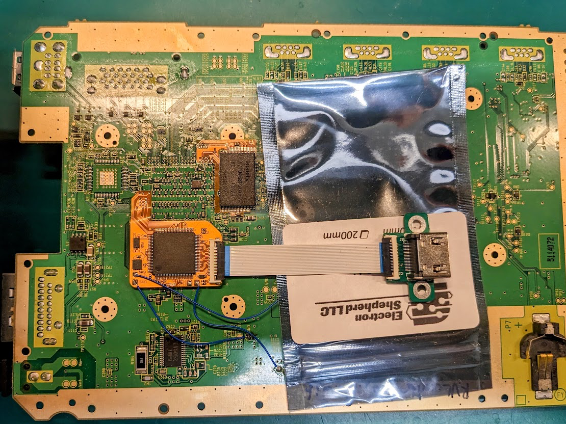
Given my requirement for robustness, I really wanted to keep the Wii motherboard mounting holes so my trim was more like an Omega Max.
Wii “Daughterboards”
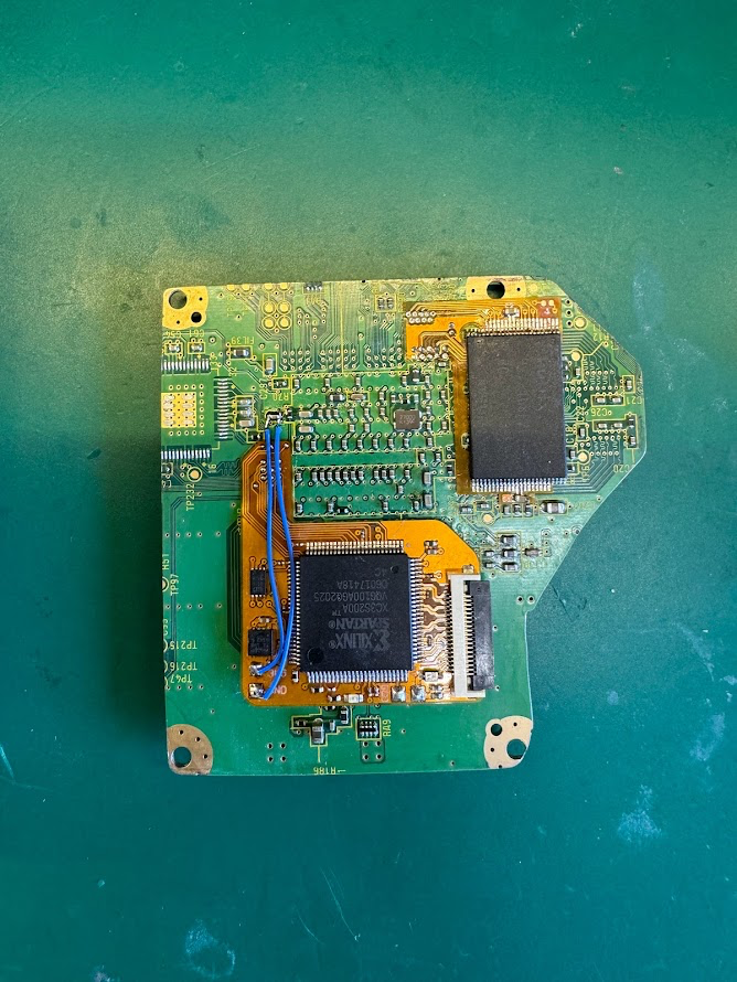
The first step was to design a couple of modular “daughterboards” which mount directly to the Wii motherboard. The idea behind these is to reduce (eliminate?) wires soldered to the Wii motherboard, and for the daughterboard designs to be usable in any project.
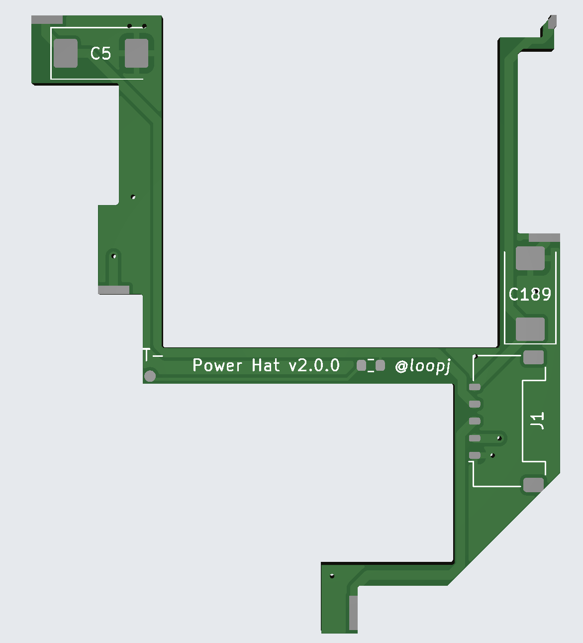
The first board is what I’m calling the “Power Strip” PCB. This mounts to the top of the Wii motherboard, and does the following
It was a real pain in the ass getting this shape just right, I 3d-printed about 15 iterations of the board outline before finding the right fit.
The second board is a “Peripheral Flex” PCB, which handles the following:
I realized after the fact that I should have also included a line for “reset”. I left a couple of lines free on the FFC to keep the BT and USB lines isolated from the gamecube lines, so I might steal one of these to send the reset signal, and run a single “fly wire” magnet wire from the back of the board to the FFC connector.
When I did a test fit of this board to a dead donor wii, I was able to get it mounted and confirm continuity between the FFC and each of the data traces, but it was a pain in the ass to solder. I’d certainly consider a redesign with larger vias.
Case design
During the design process, one of the candidate layouts accidentally had a very familiar shape - similar to the original Wii - so I decided to go all in and try to make a “Wii classic” style case design and thermal layout.
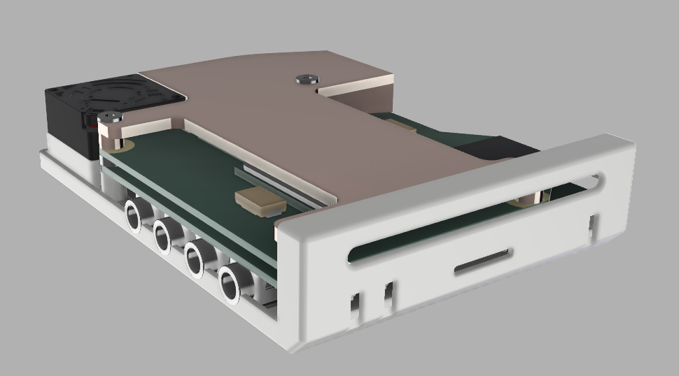
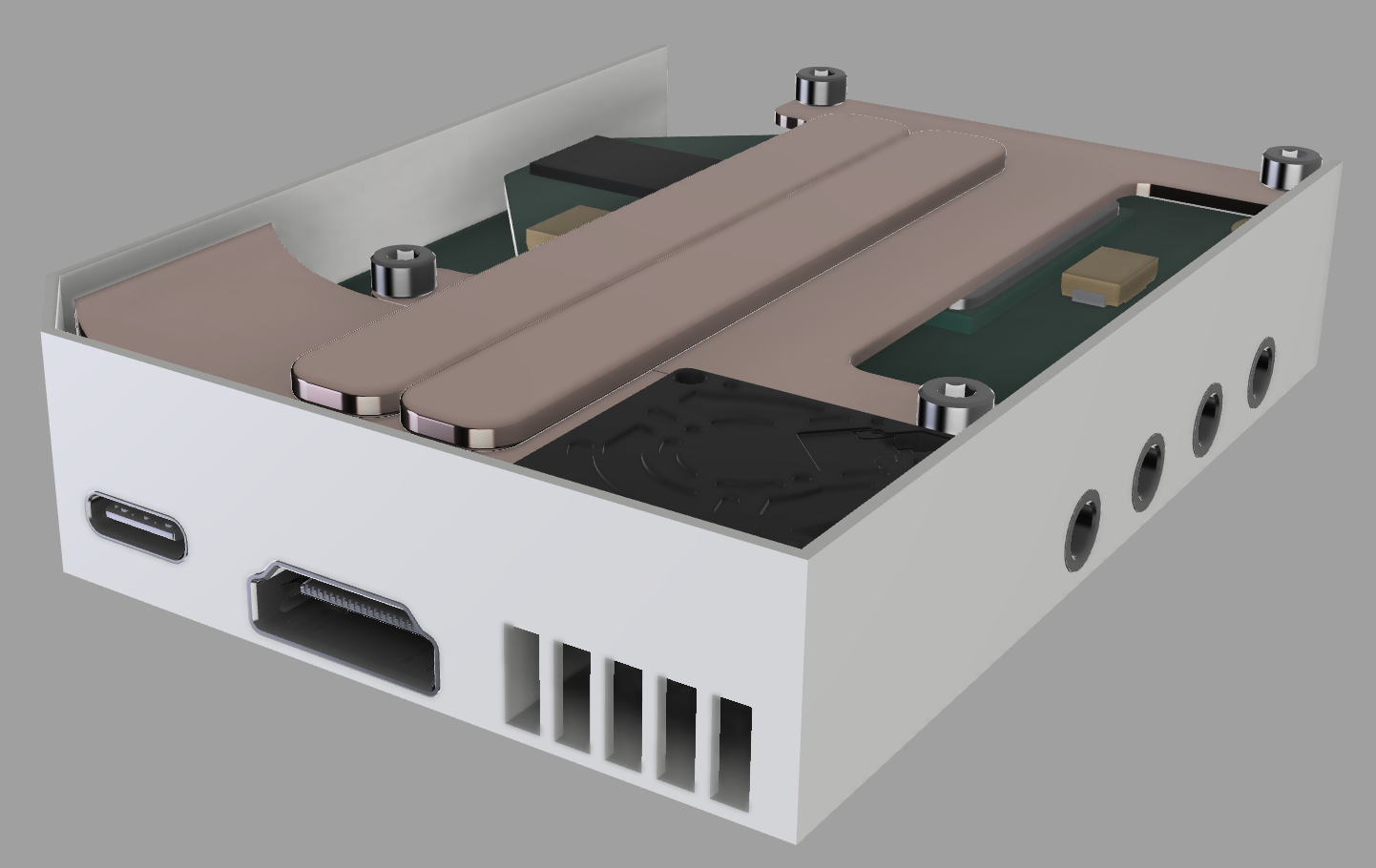
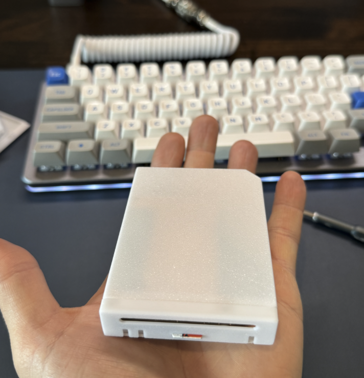
Designing this case was an absolute obsession. I wanted to ensure that it was as small as possible (~40% scale, same size as a deck of cards) without sacrificing any of the aesthetics of the original Wii. I wanted the connectors and airflow vents to be in the same locations as on the original, the microSD card slot to be where the SD card slot is on the original, and wanted to leave the top of the Wii completely clean (no holes).
The thermal design was also a big challenge - and is currently untested. I found a tiny 20x20x8mm blower fan which puts out a decent 0.84CFM at 5V - it might just do the job.
I also decided to try my hand at milling my own heat plate and heatsink, since I wanted an excuse to learn how to use my new desktop CNC.
I have so far avoided making any flaps/panels to cover the Gamecube ports or the SD card, since it is challenging to make these in such a small space. Wesk had the great suggestion to try a print-in-place or magnet attached approach, so I might try this in a future iteration.
Peripheral/power PCB
Now I know how much space I have to play with in the case, it is time to design the peripheral/power PCB.
The case design constrains both the “maximum” size of the PCB, and the locations of the connectors.
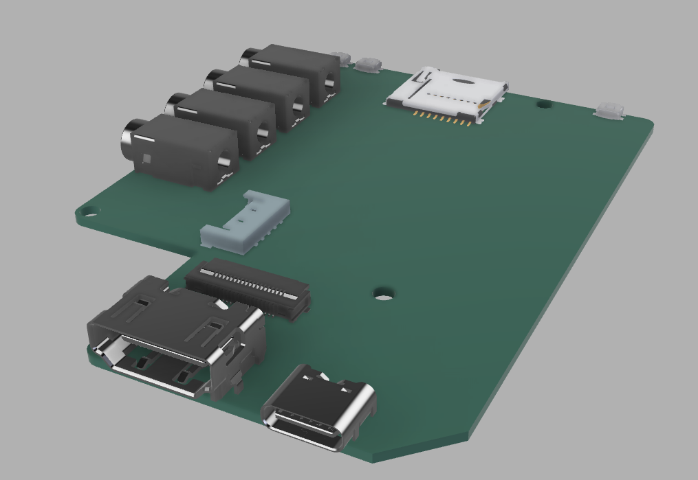
I’m making decent progress on the PCB schematic, next step is the actual PCB layout.
TODO
Thanks everyone on Discord for your help so far, I’ll update this thread as I make progress.
For the past 2 years I’ve been dreaming of building a “not so portable” with a stacked PCB design. Stacking a custom peripherals/power pcb, Wii motherboard, and heatplate reminded me of a stack of pancakes, hence “project short stack”.
Requirements
I wanted to have the following requirements:
- Robust - using wii motherboard mounting holes, and minimizing magnet wires
- Modular - should be able to disassemble without desoldering
- Reliable - cooling suitable for continuous play
- Featureful - USB-C power, 4x GameCube ports, HDMI, Bluetooth, power/reset/sync buttons, microSD card
- Small - As small as possible - Omega-ish trim
“My First Omega”
This was my first attempt in doing an Omega trim, I’ve previously done OMGWTF and LMAO trims in the past.
Before trimming I did the the “wireless” U10 relocation, NAND relocation, and AVE-HDMI installation and verified everything still worked, and then it was Dremel Time™.
Given my requirement for robustness, I really wanted to keep the Wii motherboard mounting holes so my trim was more like an Omega Max.
Wii “Daughterboards”
The first step was to design a couple of modular “daughterboards” which mount directly to the Wii motherboard. The idea behind these is to reduce (eliminate?) wires soldered to the Wii motherboard, and for the daughterboard designs to be usable in any project.
The first board is what I’m calling the “Power Strip” PCB. This mounts to the top of the Wii motherboard, and does the following
- Delivers 1V, 1.15V, 1.8V and 3.3V to the motherboard
- Allows for easy relocation of capacitors
- Adds a low-profile connector for connecting/disconnecting to the power supply board
It was a real pain in the ass getting this shape just right, I 3d-printed about 15 iterations of the board outline before finding the right fit.
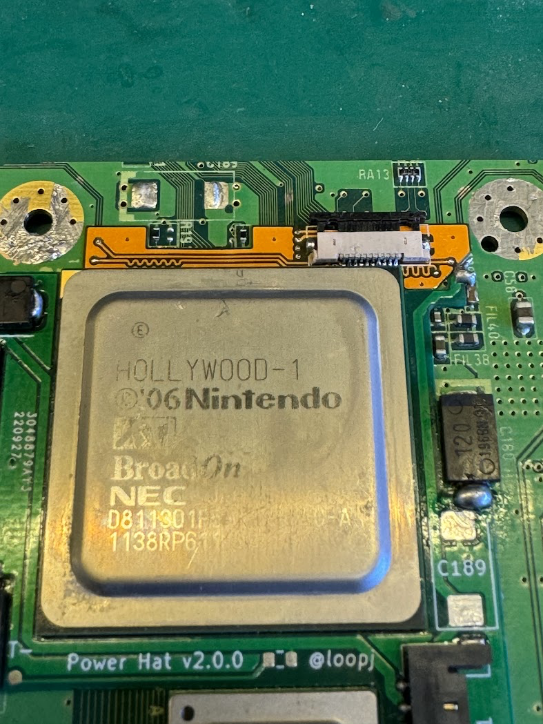
The second board is a “Peripheral Flex” PCB, which handles the following:
- Breaking out Gamecube controller data, soldering directly onto the vias
- Breaking out USB data lines
- Breaking out Bluetooth data lines
- FFC connector to send these lines to peripheral board
I realized after the fact that I should have also included a line for “reset”. I left a couple of lines free on the FFC to keep the BT and USB lines isolated from the gamecube lines, so I might steal one of these to send the reset signal, and run a single “fly wire” magnet wire from the back of the board to the FFC connector.
When I did a test fit of this board to a dead donor wii, I was able to get it mounted and confirm continuity between the FFC and each of the data traces, but it was a pain in the ass to solder. I’d certainly consider a redesign with larger vias.
Case design
During the design process, one of the candidate layouts accidentally had a very familiar shape - similar to the original Wii - so I decided to go all in and try to make a “Wii classic” style case design and thermal layout.
Designing this case was an absolute obsession. I wanted to ensure that it was as small as possible (~40% scale, same size as a deck of cards) without sacrificing any of the aesthetics of the original Wii. I wanted the connectors and airflow vents to be in the same locations as on the original, the microSD card slot to be where the SD card slot is on the original, and wanted to leave the top of the Wii completely clean (no holes).
The thermal design was also a big challenge - and is currently untested. I found a tiny 20x20x8mm blower fan which puts out a decent 0.84CFM at 5V - it might just do the job.
I also decided to try my hand at milling my own heat plate and heatsink, since I wanted an excuse to learn how to use my new desktop CNC.
I have so far avoided making any flaps/panels to cover the Gamecube ports or the SD card, since it is challenging to make these in such a small space. Wesk had the great suggestion to try a print-in-place or magnet attached approach, so I might try this in a future iteration.
Peripheral/power PCB
Now I know how much space I have to play with in the case, it is time to design the peripheral/power PCB.
The case design constrains both the “maximum” size of the PCB, and the locations of the connectors.
I’m making decent progress on the PCB schematic, next step is the actual PCB layout.
TODO
- Design the power/peripheral PCB layout and get the board fabbed
- Attach the peripheral flex to my Omega
- Mill the heatsink
- Ensure thermals actually are sensible
Thanks everyone on Discord for your help so far, I’ll update this thread as I make progress.
Last edited: