Worklog Can someone help check my work

GingerOfOz

no wario
Staff member
.
.
2020 2nd Place Winner
2022 3rd Place Winner
Joined
Dec 16, 2016
Messages
1,122
Likes
2,700
Location
The Oregon Wildlands
Portables
just so many i am so cool
Uh, every single one of those solder joints except for the one one ground is certainly a short. You solder joints need to be much smaller, that blob of solder underneath the orange component is the biggest problem right now.
 

Gabobo

.
Joined
Jan 28, 2020
Messages
62
Likes
20
Real talk, I burned off the r71. Do I have to restart all over again?
EDIT: I'm gonna start all over again. Completely destroyed the battery's solder pads + R71 which I'm assuming is mega important. Also I JUST saw the via in between those pads. Beyond that, I actually had it working before without trying to connect the sync function, which, in hindsight, was probably how I shorted the damn thing to begin with. It probably fried the 3.3v battery and permanently messed it up. Now this time I'm going to wait another week for another try.

Now for some quick questions. How does connecting the sync function work when there's only three points to solder 3.3v to? Are there other points that lead up to the 3.3v line without vias?

And since GingerofOZ mentioned the size of the solder joints, how small should the solder joints realistically be? Not as an attack but because I was soldering like mad and everything magically worked until I tried to connect the sync function.

Also: How hot should the hot air station be to remove components cause unsoldering them ain't working out seeing as it's nintendo stuff.
 
Last edited:

Stitches

2 and a Half Dollarydoos
Staff member
.
.
Joined
Feb 5, 2017
Messages
3,776
Likes
2,982
Location
Banana Bender Land, Australia
Portables
6
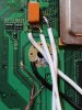
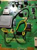
Consumer electronics use lead free solder, which has a higher melting point than the leaded solder you're probably using. For hot air removal I use 400-420 degrees F on 60% air flow with the big 858D nozzle, and small things like U9/U10 come off in 10ish seconds depending on how close you hold the nozzle.

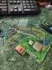
For removing stuff like U9/U10 without hot air, the best way is to add heaps of your own solder to the legs until both sides have big blobs. Then you heat both sides by quickly swapping your iron between them until you can pull the chip off with tweesers. It shouldn't take too long to do that way, but you can keep trying until you get it with little risk. Unless it takes you more than a minute, then it's probably dead.

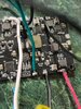
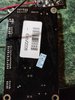
Lastly for solder joints, you want the minimum amount of solder to hold a good well heated joint. Your joints are visibly dull, lumpy, and stringy, which means your iron isn't hot enough/isn't heating the joint fully, and your tip is probably too big. Also, you're exposing way too much wire, you only need a few mm of exposed wire to tin. Exposing too much is bad practice and just asking for shorts.

Btw why are you soldering to those resistors? You don't need to connect anything there.
 

Gabobo

.
Joined
Jan 28, 2020
Messages
62
Likes
20
Got it. I had some practice after completely wrecking the board. As for the resistors, I was looking hard at the Trimming guide's pictures and the highlighted parts were on those pads... After looking verrrry closely at my mistake, I see a hole. I'm surprised it initially worked but more than that, I'm a little confused on how to wire it now. I see 3 vias for 3.3v but if I need to sync up extra Wiimotes, I'd need 4 points to wire up to 3.3v, right? I see the Trimming guide has a different 3.3v hole for each part. This is only for Bluetooth.

You're right about the solder tip being a bit larger. I was watching that video guide about soldering and I saw that the round pencil-like tip was considered "the best all round" tip for overall performance or whatever. I'm trying to keep it small but the truth is... I suck... and the wires keep flying off after soldering them. I also get super paranoid about the data wires on the Bluetooth so I scratch some mask off the edge of the lines (without scratching off the trace), just to keep a solder-like pad around to hold it down. Small joints feel so easy to accidentally pull off. I'm guessing it's the heat that makes it super durable?
Just so I have the method down, first you slap some flux on so the board doesn't get fried, second tin the tip of the wire and the soldering iron, and third put a tiny ball of solder and tippy-tap the joint on the board where the wire meets, right?

I'm not worried about the U10's/U9's cause I've been doing that the entire time. I have a stock of 4 usable U10/9 now. I also have a new MX chip to use. I'm more worried about the Memory Card slot/Power Supply/Video Out components that are just super soldered from the bottom.

EDIT: I just took a look at the compendium using Paint.NET (https://bitbuilt.net/forums/index.php?threads/wii-rvk-01-compendium-released.93/) and it looks like my question has been answered. There's 3.3v vias all over the place and one of the extra vias is literally the hole next to the one highlighted in the Trimming guide. I guess the only thing to do now is to wait for my next wii to arrive and getting my iron to spit hot fire. I should crank up the heat to a level 4-5 on my soldering station. I was using level 1 all this time.
 
Last edited:

jefflongo

Broke BitBuilt
Staff member
.
.
Joined
Dec 15, 2016
Messages
1,017
Likes
1,361
Location
Santa Barbara, CA
Portables
3
I see 3 vias for 3.3v but if I need to sync up extra Wiimotes, I'd need 4 points to wire up to 3.3v, right? I see the Trimming guide has a different 3.3v hole for each part. This is only for Bluetooth.
The 3.3v points on the bluetooth module are connected in parallel. The best way to do it is to connect them all on the module, then connect a single 3.3v wire to the wii motherboard. Also don't solder to the vias if you don't have to, it just makes the work harder. There are plenty of easier 3.3v points to solder to.

You're right about the solder tip being a bit larger. I was watching that video guide about soldering and I saw that the round pencil-like tip was considered "the best all round" tip for overall performance or whatever.
Conical tips are good, but personally I prefer a thin chisel tip for most things. Like the default tip that comes with the Hakko FX888D.

I'm trying to keep it small but the truth is... I suck... and the wires keep flying off after soldering them.
you need to hold the wire as you are soldering it. Get the wire in the right position, hold it with your non-dominant hand, and apply the soldering iron with your dominant hand. Keep holding it for a few seconds after you've soldered the wire. You should only need to apply heat for around 1-2 seconds to get the solder joint. A good solder joint (even for the bluetooth trace) should be able to withstand a decent tug on the wire without breaking, and should not be able to twist if you bend it. It also requires very little solder.

I also get super paranoid about the data wires on the Bluetooth so I scratch some mask off the edge of the lines (without scratching off the trace), just to keep a solder-like pad around to hold it down. Small joints feel so easy to accidentally pull off. I'm guessing it's the heat that makes it super durable?
To be honest I have no idea what you are saying. If you're saying you scratch off soldermask on the area around the trace, definitely do not do that. The area around the trace is ground, and if any of the ground touches your bluetooth trace, it won't work. A well soldered joint is not that easy to break off. What makes it durable is the solder flowing to both the trace as well as the wire, and good contact between them. This is hard to do because the trace and the wire are small. It's easy to heat only the wire or only the trace, but not both while keeping the wire still. If you do not do this then yes it will be fragile.

Just so I have the method down, first you slap some flux on so the board doesn't get fried, second tin the tip of the wire and the soldering iron, and third put a tiny ball of solder and tippy-tap the joint on the board where the wire meets, right?
Flux has nothing to do with the board getting "fried". If anything on your board is getting "fried" then your temperature is way too high. I use 315C which is suitable for most tasks. Flux removes oxidation from solder so that you get a consistent and durable solder joint. You might notice sometimes solder joints look "spiky" or not smooth. Adding flux will solve this.

I'm not worried about the U10's/U9's cause I've been doing that the entire time. I have a stock of 4 usable U10/9 now. I also have a new MX chip to use. I'm more worried about the Memory Card slot/Power Supply/Video Out components that are just super soldered from the bottom.
Are you trying to keep these? Because if you are it's better to just cut the piece of the PCB out that contains it instead of trying to desolder it.
 

Gabobo

.
Joined
Jan 28, 2020
Messages
62
Likes
20
Wait hold up. So basically, I'd have to keep the wire and the trace together after soldering for 1 - 2 seconds longer. Like really heat it up and then pull away. And flux keeps those joints from looking like it's rusted and gross, which also makes it more consistently durable and I shouldn't be afraid of keep the iron on for a few seconds longer to really heat up both the trace and the wire, correct?

Also you mentioned connecting all them Bluetooth points on the module first and then connecting them all to a single 3.3v point with one wire. This one interests me more as I was ready to find all the vias and solder them all to vias. Would it be like connecting a bunch of wires onto the Bluetooth module as separate wires and then merging them into another single wire? Or would it be one thicc wire that's separated into 3/4 different hydra heads? I feel like it would be closer to the the former since splitting a wire is exposing it more and that seems to be a big no-no cause it makes shorts.

Also, I didn't know the stuff outside the traces would be GND. That's very interesting and important information for me and I actually learned something new.

Edit: Don't worry about the u10/9s. Half of them are still on the board and the other half is taped on a card, in a plastic bag, safe and ready to use for the next wii

EDIT2: I figured out what you meant just now. So for the Bluetooth, you basically, connect all the 3.3v pads to one 3.3v pad and use that 3.3v pad to connect to the motherboard. Let me know if I got that right. I think it might save me from future headaches.
 
Last edited:

jefflongo

Broke BitBuilt
Staff member
.
.
Joined
Dec 15, 2016
Messages
1,017
Likes
1,361
Location
Santa Barbara, CA
Portables
3
Wait hold up. So basically, I'd have to keep the wire and the trace together after soldering for 1 - 2 seconds longer. Like really heat it up and then pull away. And flux keeps those joints from looking like it's rusted and gross, which also makes it more consistently durable and I shouldn't be afraid of keep the iron on for a few seconds longer to really heat up both the trace and the wire, correct?

Also you mentioned connecting all them Bluetooth points on the module first and then connecting them all to a single 3.3v point with one wire. This one interests me more as I was ready to find all the vias and solder them all to vias. Would it be like connecting a bunch of wires onto the Bluetooth module as separate wires and then merging them into another single wire? Or would it be one thicc wire that's separated into 3/4 different hydra heads? I feel like it would be closer to the the former since splitting a wire is exposing it more and that seems to be a big no-no cause it makes shorts.

Also, I didn't know the stuff outside the traces would be GND. That's very interesting and important information for me and I actually learned something new.

Edit: Don't worry about the u10/9s. Half of them are still on the board and the other half is taped on a card, in a plastic bag, safe and ready to use for the next wii

EDIT2: I figured out what you meant just now. So for the Bluetooth, you basically, connect all the 3.3v pads to one 3.3v pad and use that 3.3v pad to connect to the motherboard. Let me know if I got that right. I think it might save me from future headaches.
I think you are misunderstanding me. When you solder a wire, after you pull away the soldering iron, the solder will take some time (around half a second to a few seconds depending on the size and heat) for the solder to solidify. You want to make sure you hold the wire in place while the solder solidifies.

If you are using a decent soldering iron, you shouldn't be afraid of damaging the board by applying the soldering iron. If your iron is ripping up pads or burning the PCB while the temperature is properly set, trash it and get a new one. Given that you mentioned your soldering iron only has temperature "settings" and there's no way for you to know the actual temperature, this might be the case.

It would be like daisy chaining the 3.3v wires on the bluetooth module, as they are connected in parallel. Personally for me, I connect one wire from the first pad to the second, then a wire from the second pad to the third, etc. The bluetooth module doesn't draw much current, so it doesn't need a thick wire. Probably 26awg would suffice.
 

Gabobo

.
Joined
Jan 28, 2020
Messages
62
Likes
20
Alright. Yes. Thanks for really clearing that up. That actually helps a lot. I can see now how much of a caveman I was before. I was trying to solder up a little to secure the joint but that messed things up even further. Then to make things worse I went from 1 to 8 because I thought most heat was good. That's probably when I fried the resistors and every pad surrounding it.

I'll see y'all next time I get stuck (in a week). Don't worry, I read the Compendium now and I'm seeing many more spots for placement. In the meantime, I guess I'll practice wiring things on my busted boards. Peace out.
 

Stitches

2 and a Half Dollarydoos
Staff member
.
.
Joined
Feb 5, 2017
Messages
3,776
Likes
2,982
Location
Banana Bender Land, Australia
Portables
6
Alright. Yes. Thanks for really clearing that up. That actually helps a lot. I can see now how much of a caveman I was before. I was trying to solder up a little to secure the joint but that messed things up even further. Then to make things worse I went from 1 to 8 because I thought most heat was good. That's probably when I fried the resistors and every pad surrounding it.

I'll see y'all next time I get stuck (in a week). Don't worry, I read the Compendium now and I'm seeing many more spots for placement. In the meantime, I guess I'll practice wiring things on my busted boards. Peace out.
You have a good learning attitude my dude, I'm sure you'll do much better the second time around.
 

Gabobo

.
Joined
Jan 28, 2020
Messages
62
Likes
20
Back from the dead. Sorry, I was busy... training... and real life kicked my ass. I built myself a little PiGRRL 2 to practice soldering and learned some more stuff about soldering. Then I got into 3d printing to save myself some money so I can have unlimited case tries. Like I REALLY got into 3d printing. Printed out the Gwii and the Louii cases, just for comparison sake. I feel better about soldering and got myself two wiis so I can have extra tries in case something goes horribly wrong. Decided on a whim to ditch the MX chip to save myself some headaches and came back with many more questions. Since it's quarantine around my area, I figured that I have all the time in the world to do this.

1) I see battery holders on some of y'all builds. Would any soldered scrap metal be good enough to transfer the power from the batteries or is it something special I have to get online? I could probably 3D print a holder to keep it together, I was just wondering how it would work out.

2) Jefflongo brings up the point about daisy chaining 3.3v wires for the Bluetooth. Are there any other things that could be connected like that or is it just the Bluetooth?

3) I understand the buttons for the GC+ must connect one data cable to the pad and another to the GND. Would they all share the same GND or can it just be any GND on the Wii motherboard?

3.5) Also, after all the buttons are basically on the GC+ where would it go? The trimming guide points to a tiny little area with 4 data points but I would like to know for sure how I would need to hook up the GC+. I got the 1.0 and I have no idea how it would get connected.

Sorry if I sound annoying, but my mistakes are starting to get a little expensive...

EDIT: Ignore this I found all my answers by just thinking about it. Data 1 is literally Player 1. I just followed the line. I also took a look at how other people hooked up the battery (After frying the PMS) and found out that all GND is good GND. I dunno. Correct me if I'm wrong.
 
Last edited:

Gabobo

.
Joined
Jan 28, 2020
Messages
62
Likes
20
Alright now I really feel annoying. So while I wait for the new PMS, I thought I would finish hooking most of the grunt work together and see if miracles can happen. I know for a fact that I saw a guide on this forum with someone using this exact screen. My question is, can someone help me clarify the process here? I think I would have to flip it to the back and wire whatever I see to the motherboard.

On a separate note, there is a need for the vsys to be connected from the USB-C board. Do I just connect that to the box?

Take your time answering there's no rush.
 

Attachments

jefflongo

Broke BitBuilt
Staff member
.
.
Joined
Dec 15, 2016
Messages
1,017
Likes
1,361
Location
Santa Barbara, CA
Portables
3
Vsys from the USB c board just be connected to Vsys on the PMS. It powers the USB PD circuit when the system is off. Check the PMS description. For the screen, yeah, you would connect video and ground to the points listed on the board. The screen probably needs to be modded to be powered by 5v (bypass the 5v regulator on board).
 

Gabobo

.
Joined
Jan 28, 2020
Messages
62
Likes
20
Okay, I took a look at a whole bunch of cleaner looking worklogs and self-confidence aside, it looks like in order to mod the 5v from the board, I have to remove only one component from the board and it'll be ready to go from that pad to the 5v right? I see it in other worklogs but also I know I saw it in a guide that I can no longer find. It's the one marked "330" right? EDIT: STOP! DON'T ANSWER THIS! I FOUND IT!

Also, am I allowed to share 5v pads on the PMS for both the USB-C and the LCD?

Thanks for answering BTW. I know people here are busy so I'll try to keep my posting at minimum now.
 
Last edited:

jefflongo

Broke BitBuilt
Staff member
.
.
Joined
Dec 15, 2016
Messages
1,017
Likes
1,361
Location
Santa Barbara, CA
Portables
3
You can check the guide hub for a generic guide on how to mod displays to run on 5v. Generally, you insert 5v at the output of the 5v regulator on the board, and either remove the regulator or remove a series component like an inductor on the 5v line to prevent injecting current into the output of an unpowered regulator. And yes, you can share the 5v pad.
 

Gabobo

.
Joined
Jan 28, 2020
Messages
62
Likes
20
Damn, you keep presenting me with more options. So my first gut reaction is to find and remove this 5v regulator but in your opinion, which one would be better? Removing inductor or regulator? I feel like they both do the same thing.
 
Top