- Joined
- Oct 22, 2018
- Messages
- 13
- Likes
- 58
- Portables
- 7
Hello everyone,
this is my third attempt at building a Windows 98 handheld. I built the first one in 2020, followed by V2 for last year's competition.
I am starting this worklog a little later than most of the other entries, but I have already spent the last few weeks researching the hardware and designing the first PCBs.
V2 was a large improvement over the original build and actually worked quite well, but it still ended up being 39 mm thick, ran fairly hot and only managed around 1 hour of battery life. It also relied on many separate modules, which resulted in more internal wiring than I would have liked.
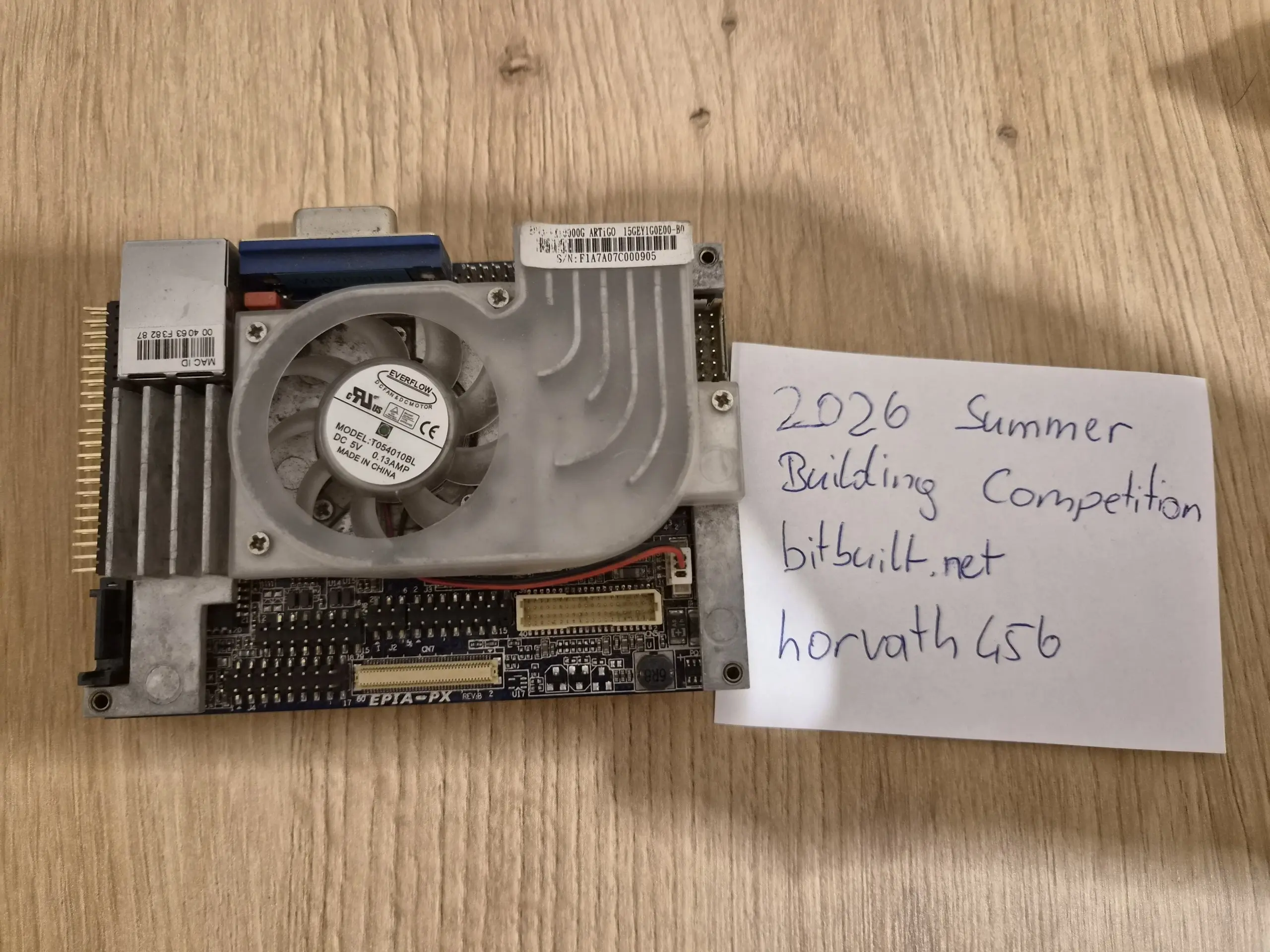
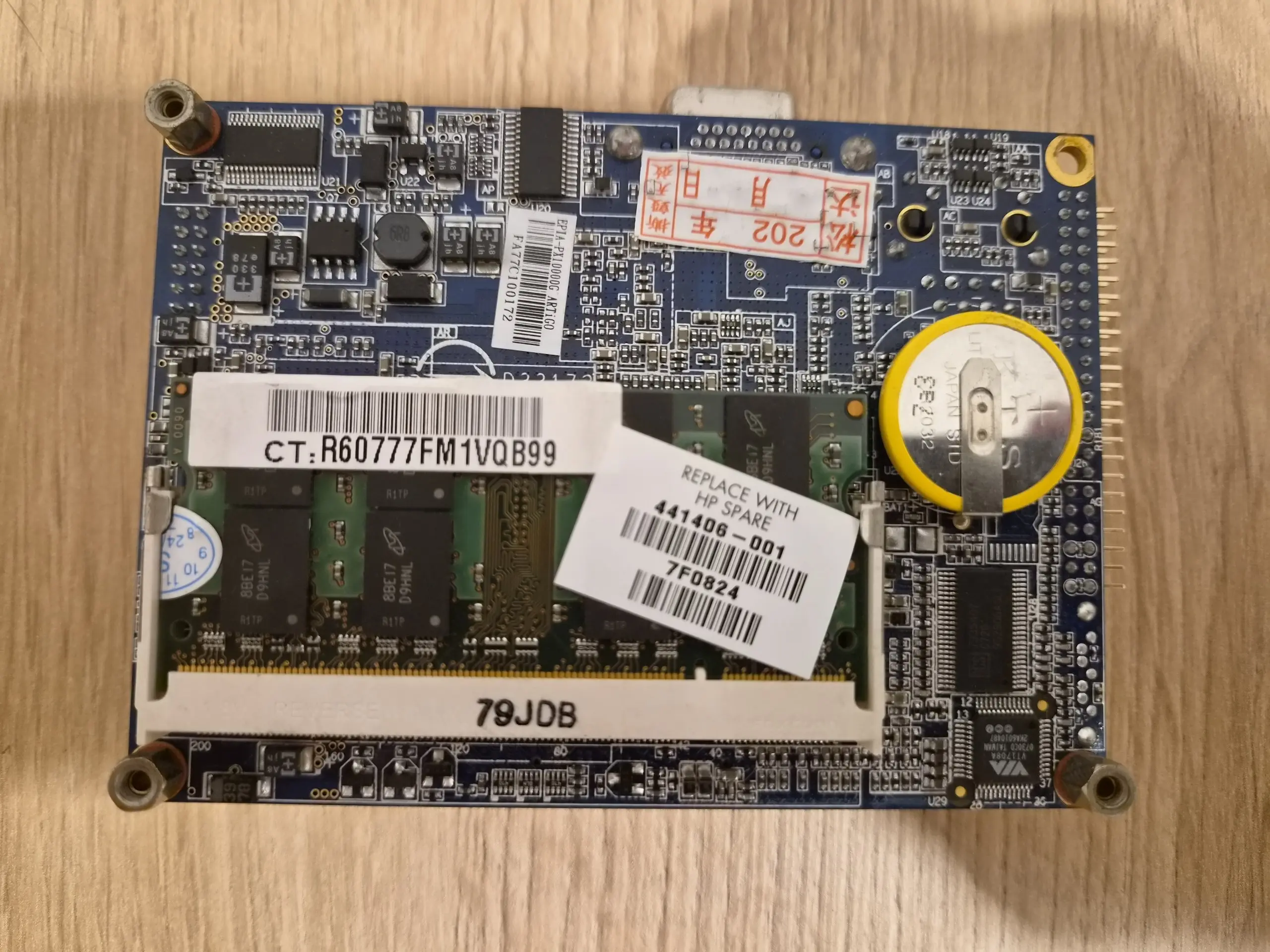
The main reason for starting V3 was finding the VIA EPIA-PX10000G. It is a complete 100 × 72 mm Pico-ITX PC with proper Windows 98 support, while being considerably smaller than the Nano-ITX board used in V2.
Rather than building another standard horizontal handheld around it, I want to use the smaller motherboard for a dual-screen clamshell.
The 6.5-inch main display will be mounted in the lid. The lower half will contain the motherboard, controls and a 3.5-inch touchscreen for additional controls and system information. The two halves will be connected using two Nintendo DS Lite hinges.
I am aiming for a footprint not much larger than a 3DS XL and as little thickness as possible.
Main hardware
The parts selected so far are:
The upper screen will be the normal Windows 98 display. The lower touchscreen will be driven by one of the RP2040s and used for game information, shortcuts, an on-screen keyboard, touchpad controls and system settings.
The second RP2040 will handle the physical controls and appear to the PC as a USB gamepad, keyboard and mouse.
Essentials
Stretch goals
Ordered PCBs
One of the main things I wanted to improve over V2 was the internal wiring. That meant I could no longer avoid designing my own PCBs.
These are not only the first boards for this project; they are the first PCBs I have ever designed. Until now, my handhelds were built mostly by connecting existing modules.
For a first PCB, the power board became quite ambitious: a four-layer board combining a 4S charger, fuel gauge, battery protection, several voltage rails and ATX power control. It eventually turned into four separate boards for power, I/O and the mechanical connection to the motherboard.
I spent a lot of time reading datasheets, checking the power requirements of the PX10000G and reviewing the layouts before ordering them. The boards are currently being manufactured by JLCPCB, and I am also using their assembly service for the populated boards. They should arrive in a couple of days, already assembled apart from a few parts that I will add myself.
I am reasonably confident in the designs (altough I just noticed I did forget some silkscreen labels), but the real test will begin when I power them for the first time.
Power board
The power board replaces most of the individual power modules used in the previous handheld. it will be glued onto the bottom side of the pixoITX board and secured with 4 ground plane solder connections.
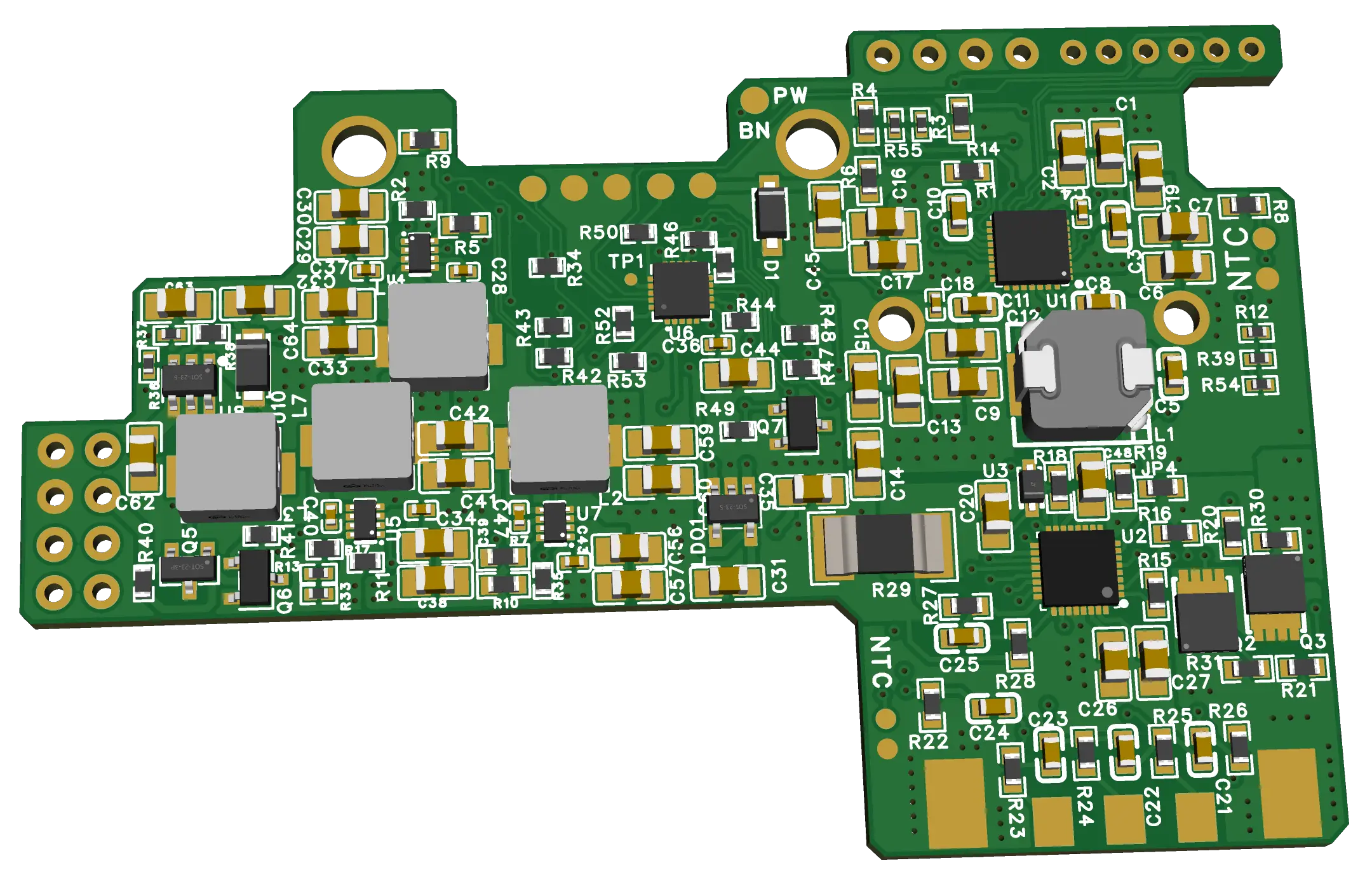
Main parts:
I/O board
The I/O board will sit along the rear edge of the lower half. It combines the ports, audio circuitry and optional radio modules on one long board.
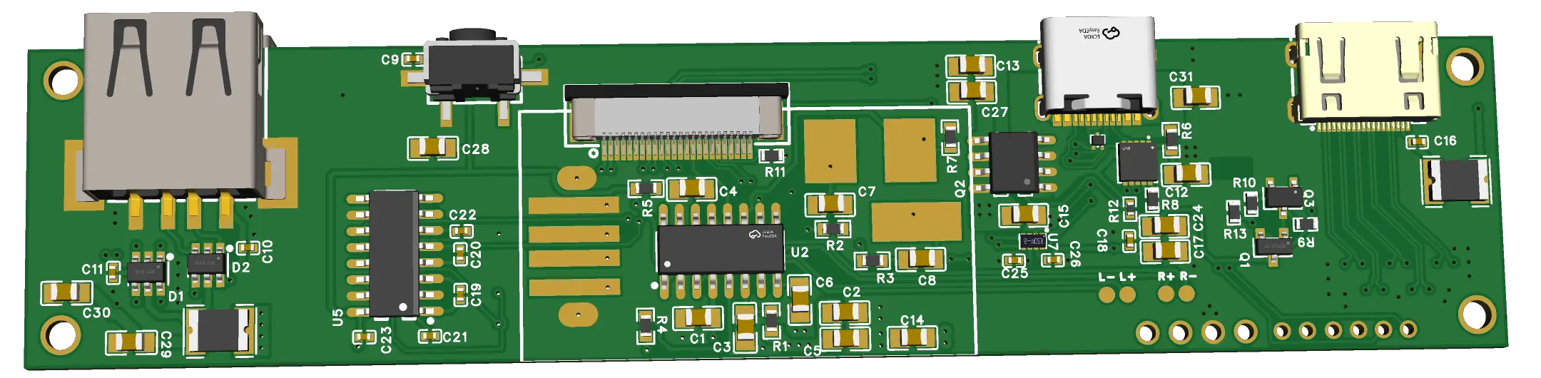
Main parts:
Power connector board
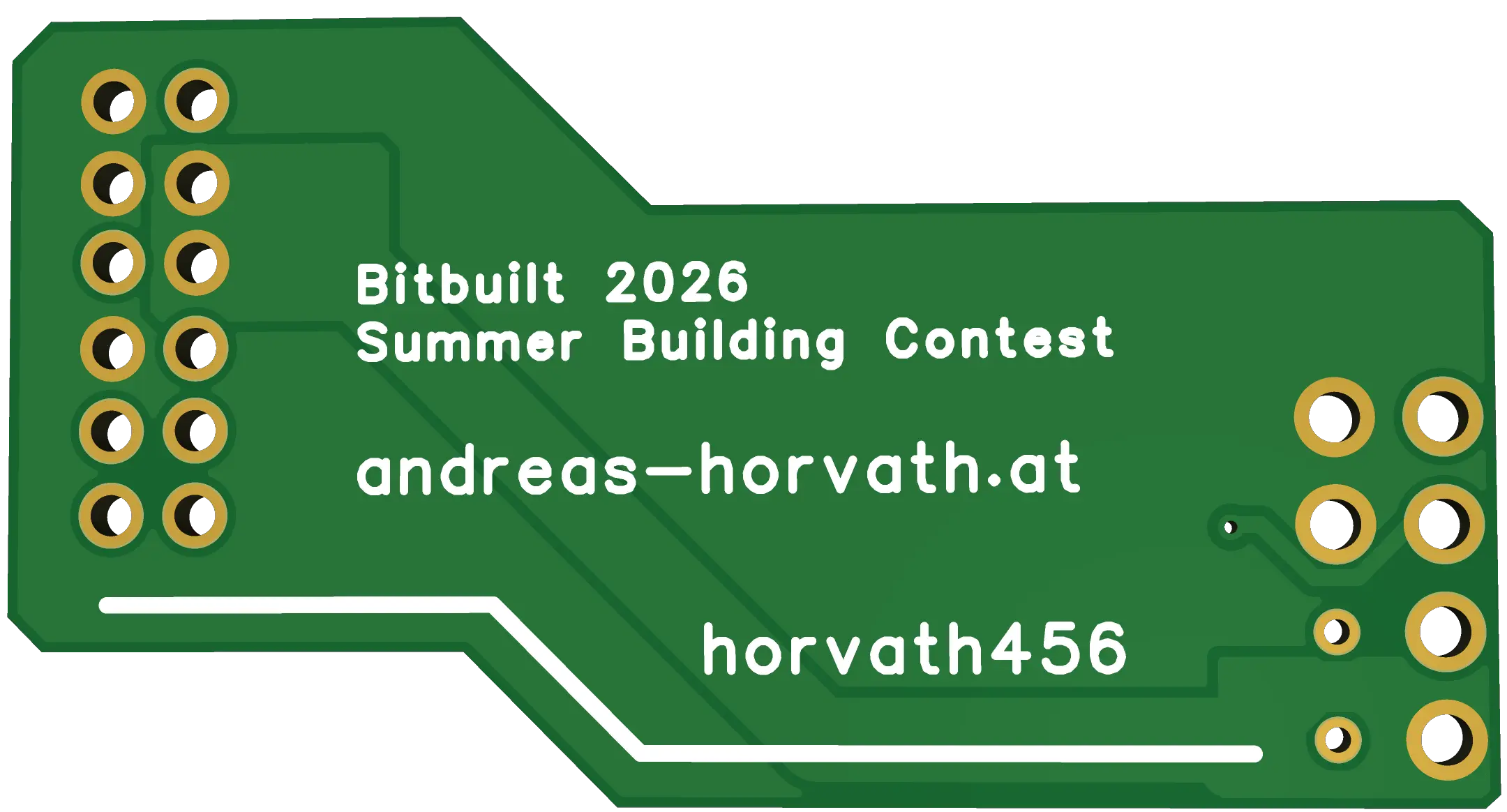
This is a small passive 4 layer board that plugs into the original 12-pin power connector on the PX10000G.
It connects the custom power board to the motherboard without needing a large bundle of wires.
I/O retention board
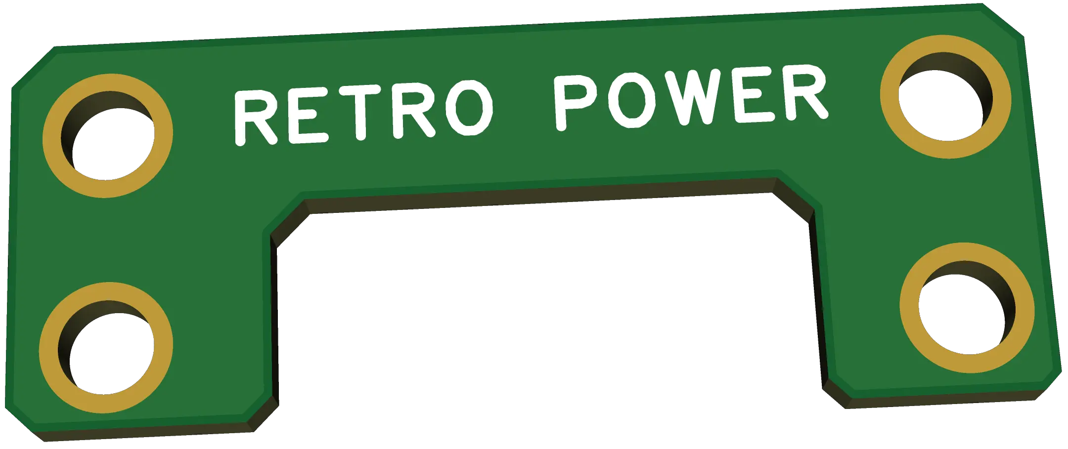
The final small board is purely mechanical. It connects the I/O board to the PX10000G assembly and helps hold both boards in position.
Next Steps
The next step is to power up the PX10000G, install Windows 98 and test its graphics, sound and power consumption.
The ordered PCBs should arrive shortly afterwards. They will come mostly assembled by JLCPCB, but still need to be tested thoroughly. The BQ41Z50 needs to be programmed and configured using TI bqStudio, I need to determine the correct register configuration for the BQ25798, and I still need to write and test the ATtiny1616 firmware. It will handle the soft power button, ATX power logic, NeoPixel status LED and serial communication.
I also need to design the custom controller PCB for the lower half of the clamshell. It will carry both RP2040s, the FFC connector for the lower touchscreen and the button contacts for the conductive rubber membranes. The two analogue sliders will sit in dedicated PCB cutouts and connect through separate 4-pin FFC connectors.
Once the motherboard and the first PCBs have been tested, I can determine the final internal layout and begin designing the clamshell enclosure.
this is my third attempt at building a Windows 98 handheld. I built the first one in 2020, followed by V2 for last year's competition.
I am starting this worklog a little later than most of the other entries, but I have already spent the last few weeks researching the hardware and designing the first PCBs.
V2 was a large improvement over the original build and actually worked quite well, but it still ended up being 39 mm thick, ran fairly hot and only managed around 1 hour of battery life. It also relied on many separate modules, which resulted in more internal wiring than I would have liked.
The main reason for starting V3 was finding the VIA EPIA-PX10000G. It is a complete 100 × 72 mm Pico-ITX PC with proper Windows 98 support, while being considerably smaller than the Nano-ITX board used in V2.
Rather than building another standard horizontal handheld around it, I want to use the smaller motherboard for a dual-screen clamshell.
The 6.5-inch main display will be mounted in the lid. The lower half will contain the motherboard, controls and a 3.5-inch touchscreen for additional controls and system information. The two halves will be connected using two Nintendo DS Lite hinges.
I am aiming for a footprint not much larger than a 3DS XL and as little thickness as possible.
Main hardware
The parts selected so far are:
- VIA EPIA-PX10000G Pico-ITX motherboard
- 6.5-inch AT065TN14 TFT with HDMI/VGA controller board
- 3.5-inch Waveshare capacitive touchscreen
- Two Nintendo DS Lite hinges
- Four 18650 cells
- Two 3DS analogue sliders
- Two RP2040 microcontrollers
- Custom power, I/O, control and interconnect PCBs
The upper screen will be the normal Windows 98 display. The lower touchscreen will be driven by one of the RP2040s and used for game information, shortcuts, an on-screen keyboard, touchpad controls and system settings.
The second RP2040 will handle the physical controls and appear to the PC as a USB gamepad, keyboard and mouse.
Essentials
- A functional dual-screen Windows 98 clamshell handheld
- A footprint close to a 3DS XL and as little thickness as reasonably possible
- Windows 98 SE running natively on the PX10000G
- Integrated gamepad, keyboard and mouse controls
- USB-C charging and charge-and-play
- Internal speakers, storage and active cooling
- Custom launcher and companion interface
- Custom PCBs instead of separate power and interface modules
Stretch goals
- Wi-Fi with an ESP8266 module acting as a Hayes-compatible modem (just like the WIFI232)
- Bluetooth audio
- External HDMI output (still unsure whether the motherboard properly supports DVI out)
- Nintendo 64 and GBA emulation (not sure the board can handle smooth emulation)
- Correct display output across the different resolutions used by DOS and Windows 98 games
- Updating both RP2040s firmware without opening the enclosure
- almost wire-free design
Ordered PCBs
One of the main things I wanted to improve over V2 was the internal wiring. That meant I could no longer avoid designing my own PCBs.
These are not only the first boards for this project; they are the first PCBs I have ever designed. Until now, my handhelds were built mostly by connecting existing modules.
For a first PCB, the power board became quite ambitious: a four-layer board combining a 4S charger, fuel gauge, battery protection, several voltage rails and ATX power control. It eventually turned into four separate boards for power, I/O and the mechanical connection to the motherboard.
I spent a lot of time reading datasheets, checking the power requirements of the PX10000G and reviewing the layouts before ordering them. The boards are currently being manufactured by JLCPCB, and I am also using their assembly service for the populated boards. They should arrive in a couple of days, already assembled apart from a few parts that I will add myself.
I am reasonably confident in the designs (altough I just noticed I did forget some silkscreen labels), but the real test will begin when I power them for the first time.
Power board
The power board replaces most of the individual power modules used in the previous handheld. it will be glued onto the bottom side of the pixoITX board and secured with 4 ground plane solder connections.
Main parts:
- BQ25798 buck-boost battery charger
- BQ41Z50 fuel gauge, cell monitoring, balancing and battery protection
- ATtiny1616 for power sequencing, power-button handling and status communication
- ATX PSU control circuitry and power converters built in
- Connection for the four-cell battery pack
I/O board
The I/O board will sit along the rear edge of the lower half. It combines the ports, audio circuitry and optional radio modules on one long board.
Main parts:
- HUSB238A USB-C Power Delivery controller
- PAM8406 stereo class-D speaker amplifier
- USB sound card connection
- MAX3232 interface to the PX10000G serial port
- ESP-01 footprint and control circuitry for Wi-Fi
- KCX Bluetooth audio module connection
- USB-C connector
- External USB connectors
- Mini-HDMI connector
- Power button
- Speaker connections
- 24-pin FPC connector to the lower touchscreen/controller board
- Resettable fuses for the USB and HDMI power outputs
Power connector board
This is a small passive 4 layer board that plugs into the original 12-pin power connector on the PX10000G.
It connects the custom power board to the motherboard without needing a large bundle of wires.
I/O retention board
The final small board is purely mechanical. It connects the I/O board to the PX10000G assembly and helps hold both boards in position.
Next Steps
The next step is to power up the PX10000G, install Windows 98 and test its graphics, sound and power consumption.
The ordered PCBs should arrive shortly afterwards. They will come mostly assembled by JLCPCB, but still need to be tested thoroughly. The BQ41Z50 needs to be programmed and configured using TI bqStudio, I need to determine the correct register configuration for the BQ25798, and I still need to write and test the ATtiny1616 firmware. It will handle the soft power button, ATX power logic, NeoPixel status LED and serial communication.
I also need to design the custom controller PCB for the lower half of the clamshell. It will carry both RP2040s, the FFC connector for the lower touchscreen and the button contacts for the conductive rubber membranes. The two analogue sliders will sit in dedicated PCB cutouts and connect through separate 4-pin FFC connectors.
Once the motherboard and the first PCBs have been tested, I can determine the final internal layout and begin designing the clamshell enclosure.
Last edited: