Hi all! Back in 2021, I joined the BitBuilt community and tried my hand at portabilization with the GameBoy Adwiince v2. It even snagged 2nd place in the summer competition, despite the fact that the project crashed and burned on the very last day. I shorted the power supply during final assembly, and it never booted again.
Reminder for v2. I'll do a little retro in a next post.
Still, that project was what got me into electronics. I learned a ton, and even switched career from game development to now being a second-year electronics engineering student. I've worked on other projects, kept learning, designing my own PCBs, and yet I kept thinking back to the build that started it all. And I thought... Revenge!
I want revenge!
I want to try again, with all the new skills I’ve picked up, and see how far I can push it this time.
The goal is still the same: cram a Wii into a GBA form factor with a 5" screen. Last time, I tried frankencasing, and while that was fun, constantly measuring, sanding, measuring, sanding, measuring, gluing, desparing when it didn't fit XP Final assembly was a nightmare no proper screw holes, nothing aligned, and everything needed copious amounts of glue which left a residue and was not strong enough, and it took up a lot of time I should probably have used on the electroincs side of things.
This time, I’m doing it simple: fully 3D modelled and printed. I can get it to look like I wanted to begin with, can prototype more, and can model in stronger better mounting solutions. Though I will not give up the colored translucent shell look from the original build, that 2000s GBA feel. So I'll probably ask a friend, or send it off to a company, to resin print the final version.
Where I really want to focus is on PCB design. Last time I just dipped a toe in, designing a simple backplane to make wiring easier. This time, I’m going deeper: I want to move as much onto custom PCBs as I can. Power supply, USB PD, BMS, you name it. I’ll be referencing open-source designs, modifying them, and soldering everything up myself.
It’s a big project, and I’ll be balancing it with work over the summer. But I think it’s going to be a really fun challenge, and if all goes well, I’ll finally get my revenge... and a working handheld this time. ^^
Alright, time to revive a project that’s been marinating in a box for four years. Here's where I left off, what broke, and how I plan to actually make it work this time.
First off, it’s not in great shape. The back split open because the glue didn’t hold, I’m missing the shoulder buttons, some of the wiring has come loose... and yeah, it didn’t actually work. XP
I’ll be tearing it apart to recover some components: USB PD, BMS, audio, and the GameCube controller PCBs. I’ll use those for prototyping, and maybe reuse them in the final version - unless I decide to make custom PCBs for those features, which is the current plan.
The goal is to design my own USB PD and BMS/power supply PCBs. I need to do that for another project anyway, so this is a great excuse to start. I’ll be relying on open-source designs and poking around a bit more before diving in. For audio and controller stuff, I’ll use open-source repos and look into how best to integrating them into my board.
Back to v2.
I put a ton of time into the case - rough cuts, sanding, fitting parts in by hand. I wanted it as small as possible, so I even carved into the corners to fit the screen. Next time, I’ll 3D print the shell and make the screen sit properly inside the case, but still keep it snug and within the GBA form factor.
I also hated the “double chin” at the bottom. I thought about grafting parts from a third GBA shell to smooth it out but ran out of time. This time, I’ll model it so the bottom either continues the curve or just flattens. Might print both and see what looks better.
Since the original GBA shell only had two buttons (A and B), I had to cut a hole and add another set for X and Y. I chamfered the opening to make a lip, so pressure transferred into the plastic instead of the glue. That actually worked decently.
But the buttons didn’t feel good. The GBA uses rubber domes on PCB pads, but I had to trim the rubber to make it fit, and that made them too soft. The PCB mounting didn’t hold the rubber down properly either, which made everything mushy. Plus, the whole d-pad and rubber setup was chunky and ate a lot of space.
This time, I’m thinking Joy-Con buttons. They’re low profile, need less support plastic, and are already meant for four-button layouts.
Now for the shoulder buttons - ugh. They were a pain. The design relied on the case fitting together perfectly to hold them in place, but the frankencase didn’t align well and the shoulder buttons needed more clamping force than the fragile case could give them. The buttons popped out early and disappeared during one of my moves.
I tried doing three-stage buttons to simulate analog input - unpressed, half, full. But getting the big GBA buttons to trigger tiny SMD switches was rough. Sometimes it didn’t register a full press, other times it got stuck. The actuation distance was just too short.
For ZL and ZR, I added extra buttons with long stems poking out of the case... not elegant. For v2, I’m stealing the Joy-Con shoulder design. Way easier, and now that I’m doing full 3D modelling, I can actually integrate them instead of glue-and-hope.
Thermals? I cut fan holes in the back, around the battery lid, and used the cartridge slot as exhaust. I’ll probably do the same again, but make the cutouts look cleaner and symmetrical this time.
Ports were kind of a mess. They didn’t line up well because I had to put them wherever the PCBs allowed. I had USB-C for power and a bunch of mini-jacks for GameCube controller output, component video, and audio. I thought about using the GBA-to-GameCube link adapter to combine stuff into one port, but ran out of time and just went with mini-jacks.
For this version, I might go with dedicated ports or try consolidating them into a single multi-port setup with a breakout add-on to reduce case holes.
I also slapped infrared LEDs on the bottom so it could act as its own Wii lightbar. Just for fun, really - but I’ll probably do that again. It’s cool and functional.
Let’s talk internals.
I made two main PCBs, one per side, connected by a ribbon cable. That let me mount buttons to each board on both the right and left, with the Wii motherboard sandwiched in the middle. One side had USB PD, BMS, and audio; the other had the GameCube controller PCB and the MX chip. Each PCB acted as both backplane and button contacts.
It was my first PCB design, and I’ve learned a lot since then. I’ll make new boards for this version - probably still two boards and a ribbon cable. One thing I liked was how they followed the shell shape and had cutouts for tall components like the display controller.
Now that I’m doing full 3D modelling, I can make stuff actually fit instead of measuring and eyeballing everything IRL.
One big screw-up on the old boards: I didn’t leave enough clearance between components. Pads were too tight, and spacing was bad. Worst offender? The BMS sat too close to the Z shoulder button and caused a short - ground from the button ended up connected to the BMS. This time, I’m being way more careful with spacing.
For the Wii, I didn’t go for the hardcore NAND relocation cut because I was depth-limited and didn’t want it pressing into the back shell. Still trimmed it a decent bit to free up space.
This time, I’m thinking of going full Omega cut - give up some depth, gain more room for the PCBs. We’ll see.
Main takeaway?
Proper 3D modelling, smart component layout, and clean mounting are going to be the biggest upgrades over v2. Last time, I was boxed in by the frankencase approach - stuck with whatever fit into two glued GBA shells, and couldn’t mount hardware well because I had to cut out the posts.
Now I can expand the shell where needed, use better buttons (hi Joy-Cons), and design proper mounts. I’ve got way more experience with electronics, soldering, and PCB design now, and that’s where I want to focus: making a custom power solution, trying out undervolting, and seeing how far I can push a fully custom PCB.
What comes next?
First up: sourcing a new Wii that I can cut.
Then comes figuring out components and specs. I found a 5.5” OLED display with thin bezels that I think could be really neat to use. It’s a phone display that runs over MIPI, but it comes with an HDMI driver board.
I’m also thinking of using Fujiflex by YveltalGriffin. It lets me ditch the AVE and do a more aggressive cut. I’ve even considered modifying it and adding an option to drive the MIPI connection directly from the FPGA using something like an SN65DSI83 or LT8912 bridge. That would let me drop the chunky driver board and all its ribbon cables and adapters. Still need to do more research there. Edit: MIPI is under NDA that I don't have access to. And the bridges I was looking at want FROM MIPI to flatlink. Not TO MIPI which the the display needs. It was an interesing investigation, but in the end I was just following a ChatGPT hallucination that seemed plausable before inverstigating it further.
For NAND relocation, I’m probably going to use something like nandFlex(also by YveltalGriffin), which is based on OmegaFlex by Omega47. That way I can go full omega cut.
Power-wise, I’m planning to design a supply based on ThunderVolt (YveltalGriffin again!) and handle battery management with a system based on RVL-PMS by Gman. I’ll also need to dig a bit into how best to handle USB-C PD.
For GameCube controller support, I’ll be borrowing from GC+ 2.0 by Aurelio92. Audio will be handled through Scampi, once again courtesy of YveltalGriffin.
Finally, I’ll start CAD work: finding files for the GBA shell and Joy-Cons, then modifying them so I can print a draft case and get a feel for the design in hand.
Massive thanks to @YveltalGriffin (mackieks on github) for the absolute goldmine of open-source projects, and especially for the reference list that helped me find so many of these. Also big shoutouts to @Gman, @Aurelio, ikorb (for GCVideo), and all the other amazing modders who’ve released open-source versions of their work. Being able to build on what they’ve done makes it possible for me to design my own PCBs that combine all of these features into what will hopefully be a pretty epic console.
Edit: MIPI is under NDA that I don't have access to. And the bridges I was looking at want FROM MIPI to flatlink. Not TO MIPI which the the display needs. It was an interesing investigation, but in the end I was just following a ChatGPT hallucination that seemed plausable before inverstigating it further.
Very good, I love both doing and seeing crafts being done, I think there is no better feeling than taking something and building everything from scratch, especially the body, and before I forget Good luck!
Time for a little update. Highlights this round are trimming, and jumping into the PCB rabbit hole.
Wii and trimming
First off, got a new Wii, it was super cheap as the case was rather banged up.
Naturally, I quickly jailbroke it, and installed RVLoader.
Then the fun part of tear it down and sketching out the outline for doing a Omega trim. I also desoldered the components which might be in the way, including the NAND for NAND relocation, and the AVE. Though I’ll be using Fujiflex for HDMI instead of the original AVE and component video.
Rough cut time! Tried to be careful, cutting way outside my lines so that I could cut and sand inwards later. But… the Dremel accidentally hit some of the GPU traces. It seems like it was only the solder mask that got scuffed and exposed some of the copper. I don’t see any damage on the actual copper traces, but I will investigate closer with a microscope later. And potentially add some solder on the exposed copper to bridge any micro breaks if it turns out to be a problem.
Used to Dremel to sand in closer to the final outline. Another tiny scuff, but only on the grounding around on of the screw holes. Did the final sanding by hand before measuring the resistances, which were pretty much all spot on. Except 3.3v which was more erratic jumping around, but generally stayed about 10k~20k higher than the listed values for OMGWTF / LMAO. But seeing from other posts it seems like that should be fine.
Some comparison pictures to my previous OMGWTF trim. Damn it quite a bit smaller than I expected.
Display
The display also arrived! It’s a phone display with an HDMI driver board. It’s slightly larger than my previous EYOYO component screen, at 5.5” vs 5”. But at the same time it’s ultra-thin, with almost no bezels (It feels like it will snap if I look at it wrong, lol). And the picture looks decent so far, though I have not tested it with the Wii, or with games in general.
Display test. Only ran it for a short time to check that it worked.
Though the display comes with a really dumb adapter to go from the display connector to the FCC connector on the driver board. It has a weird 90-degree rotation, and makes it not fit at all which is really annoying. So, I might look at making my own adapter PCB, following the traces on the existing PCB, and reusing the components from it.
I also got this nifty HDMI to micro-HDMI cable, which is just two boards with HDMI to FCC and back. But I think I can just disconnect the FCC cable and slot in one from the GCVideo HDMI for testing. Though I’ll likely desolder the HDMI port, along with all other ports, and which ever power regulators I can from the driver board. And just solder on the HDMI, and voltages directly for a slimer fit.
PCB stuff (ThunderKILL)
Beyond that I also started looking at PCB design. First off, in my previous post I said I’d investigate if I could somehow output MIPI from the FPGA from GCVideo, or use a MIPI bridge, so that I could drive the display directly without the driver board/make my own driver board. Well, that seems like a dead end. I followed a hallucination that seemed plausible before I realized that the MIPI standard was under NDA. And that the bridge chips were FROM MIPI, not TO MIPI. So, I’ll be sticking with just using HDMI.
Otherwise, I did a lot of research on power, BMS, USB C PD, and a bunch of other things. Trying to figure out how much stuff can I cram into it. (The schematics in this post are just a draft/first version. I’ve not rechecked all the components or connections.)
What do you get if you take the amazing fantastic, well balanced and well planned out Thundervolt, and try to make it overkill by squeezing too many features into one single board?
Introducing the ThunderKILL!
It has I2C regulated regulators like the Thundervolt, but now including 5V boost
Current monitoring on the 4 primary voltages
BMS
USB C PD
RGB led controller
Temperature and fan controller
Power button/switch handling
All in one compact package/Wii hat!
And more BGA chips to solder, yay!
I’ll have to expand the size of the board just a tiny bit to make it fit. I'm sure this is a great idea, does not require any major sacrifices, and there won't be any thermal issues from cramming this much onto the board. If only there was a warning somewhere by someone smarter than me, and with more experience… Ah well… It’s a fun project regardless of how it turns out.
BMS saga
So I spent a lot of time on the BMS section. I first found one charge controller that I thought, “Wow, this looks amazing, look at all the features, look at how powerful and good it is. Let me spend days figuring this out. Figure of merrit, expected power loss. Scavenging Digikey to find the most optimal components”. Then as I put it all into the schematic I went, “Wait… that a hell of a lot of components” Checked the pcb view… “Damn that would almost double the size of the Thundervolt just due to the BMS. Wait the RVL BMS wasn’t that big…”. Checked the spec sheet for the charge controller used in the RVL BMS…. Aaaaaand…. Realized the obvious. More features, more powerful, does not mean better for the job it is supposed to do. It just makes it more complicated without any useful gain in this case. Nevertheless, I found a much more suitable charge controller and implemented that instead.
My overkill BMS 1S-4S, Vin 3.5-24, 8A charging.
Reasonable 1S, Vin 3.9-18V, 3A charging.
Other pcb bits and bobs
Found this tiny nifty PD sink, I just need to implement a PD policy on the Tiny. Need to do more research to make sure I can do that and don’t need to go for a standalone PD sink.
Also some general bits and bobs from current monitor, temperature/fan controller, and led controller. They are “nice to haves” but are on the list of things getting cut if they don’t pan out during the layout.
Current sensing
5V boost
LED controller, and fan/temp controller
I2C address space
Have not started on reworking the Thundervolt layout to fit all the overkill features from the ThunderKILL. I’ll be double, triple, and quadruple checking the schematics to datasheets first. Then I’ll be looking at the layout next. Along with supporting PCBs for the controller portions, audio, hdmi mux switch, MX chip, display adapter board, and whatever else.
No case progress yet beyond downloading scans of the GBA and Joy-Cons to procrastinate plan with.
And that’s the current status of this GBAWii revenge build. Next up: layout time, side boards, and eventually some actual progress on the case, maybe, perhaps, possibly.
Anyway stay tuned, and as always, RIP my free time
First off, introducing the ThunderKILL. It's the Thundervolt, but 500% more overKILL.
(Do I have enough edge connectors yet?)
Specs:
I2C controlled voltage regulators for 1V, 1.15V, 1.8V, 3.3V, 5V
Current sensing on all of them, cause why not
USB-C PD input, into an eFuse for overvoltage, overcurrent, and reverse current protection. Is it overkill? Yes. Is it necessary? Probably not. Am I paranoid enough to add it regardless? Yes absolutely!
BQ charge and battery controller, with built in current sensing, cause why not get more current data. And a resettable fuse to the battery, cause again paranoid as fuck.
Temperature and fan controller, with a temperature sensor between the CPU and GPU to control the fan. And another sensor next to the charge controller, and a last sensor on the other side of the board between regulators, cause more data is fun.
RGB LED controller, cause RGB makes things go faster! And charge/status LED is neat.
And power button input, U10, and some jumpers for safe mode, and to set the power button mode.
Any suggestions on anything more I should add to make it more overKILL? I think the PCB is still visible on the left side XP
(Also, do you spot the lucky “easter egg” cat? He’s become a mandatory feature in all my designs.)
Next up: Front shell for the GBAWii3
Current iteration:
Comparison to GBAWii2:
Earlier iteration with Joycon buttons and D-pad:
Did a few iterations to get the rough placement of the display, buttons, and joysticks, and the overall shape of the console.
The original plan was to use Switch Joycon buttons and D-pad. But I hated how they looked and felt. Way too small for the console I was building, and didn’t fit the GBA theme. So I went back to my previous design, using original GBA buttons and D-pad. Placing the buttons on the same slant as the original, and then doubling them on top to get X and Y, creating more of a rhombus shape over the traditional diamond shape of all modern controllers. And so far I like to look and feel of that way more. Though I will adjust the exact positioning as I build out the depth and can get more of a feel for holding it.
Internals part 1: Display driver board
Option A:
Option B:
It's annoying how close I'm to placing the Wii and the driver board next to each other, instead of having to layer one on top of the other.
The driver board originally came with an adapter board to change between the connector of the display to FPC. And to add in OLED power. But it's positioned horribly, so I will need to make another solution.
Option A: Make a flex PCB which fits what I need it to do. The display connector on one side, fpc pins on the other so it can connect directly in. And the OLED power in the middle. It’s a simple redesign of just the adapter board, so that I can position things correctly. And is the most reasonable option.
Option B: The driver board is using a Realtek RTD2513A for HDMI to LVDS, and a POL8903 for LVDS to MIPI. I have the full datasheet for the RTD, and a smaller spec sheet for the POL showing pinout, footprint, and voltage data. That along with the original driver board, means I could reverse engineer it… And then just make my own driver board to fit the GBAWii3 perfectly without the need for the adapter board, and without the need to stack the boards. I’d have to reuse the components from the current board as you can’t buy the POL on its own. But it would give me full control, and I could nix anything on the driver board I don't need, like more power regulators, and audio.
But of course doing this would be a bit overkill, it's a 196 pin BGA chip, needs good impedance control for the LVDS and MIPI lines, and is a lot of work… So see you when I have a draft of that done XP
Internals part 2: Everything else
(Aren't my drawing skills amazing XP)
The Wii on the right on top of the back of the display.
The driver board on the left.
A USB C and mini HDMI ports between the wii and the driver board. I’ll put a HDMI mux on there as well to switch between internal and external. And a place to mount the microSD card on top, like a mini cartrage.
Right side controller PCB, for buttons, joystick, volume wheel, mini jack, audio controller.
Left side controller PCB for D-pad, joystick, power switch.
There will be an IR light on both of them to allow for motion controls.
I placed bluetooth, MX, GC+ and GC mini jack rather arbritratily, and they will likely move around as I get to those PCBs. Oh and I need to place the speaker(s) and rumble somewhere…
Final notes
I want the shell to be translucent like the OG GBAs and my previous attempt. I always loved being able to see the insides and the PCBs.
However, with the Wii mostly covered up by the heatsink, and the need for a LiPo battery somewhere, it could limit how much you actually see… Hmm it might be an idea to hide the battery under the driver board and under the middle PCB so that the driver board and middle PCB is still out towards the back. But we will see as I CAD out the design more.
Hey, looooooooooong time no see. Work’s been eating most of my summer, but I’m back with a big dump of updates. I’ve more or less completed all the PCBs I had planned, I just need to do final checks on them. Along with good progress on the case design.
ThunderKILL
Starting off with where I was last, ThunderKILL. It has the same features as last time, but I reworked the layout so that most of the power outputs are on the left side, to be more accessible by other boards. And more of the control signals on the right side. Also made a github page for it.
RainbowBRIDGE
I talked about wanting to minimize the driver board last time. And now I have done it! I looked into the RTD2513 which is a HDMI to LVDS chip, and the POL8903 which is a LVDS to MIPI chip, which together gives me a neat HDMI to MIPI bridge. I looked into all the other components on the driver board and ended up killing most of them. Onboard power regulation? Don’t need that, I can supply power from the ThunderKILL. Touch screen features? Nope. Audio? Nah, no thanks I’m good. And so on, until I was left with only the minimum amount of components needed to make it run, making my version, the RainbowBRIDGE, tiny in comparison. I also moved the OLED power regulators onto my board instead of having a useless daughterboard and making it so the driver board just clips directly onto the display. With all the cutting of features I added a single new feature, which is the option for hot plug detection, where the display can be turned off if you are muxing the signal out to an external display. In the end my version of the driver board ended up being the size of the old daughter board, a tiny 25x40mm vs the original 56x90mm.
Here is the github project for it. My hope is for it to be a more generic project where if others wanted to use the same 5.5” OLED panel, they could use the RainbowBRIDGE to minimize the driver board as much as possible. But however, it relies on that you are able to relocate the 196 pin BGA POL chip, and the RTD, so it is not an easy operation...
MelonLORD
Now while ThunderKILL and RainbowBRIDGE were developed to be more generic boards which can be used by others when I’m done developing them. These next ones are boards specifically for this project as support boards, acting to connect all the pieces together, and for buttons and ports and stuff.
First up is the MelonLORD! It is using the MelonHD by YveltalGriffin to get USB-C DP out, as such it also has a HDMI MUX to switch between using the internal display and the external USB C connection. I also put a SD to USB bridge on it, using the USB2244 from Microchip. I’m not sure if the Wii will accept it or not, but thought it was worth a try, I have a backup SD to USB from Electron Shepherd that I can use in case it does not work. (They sold them back when I did the GBAdwiince v2, but no longer sell them…)
This is the right-side controller board for buttons and joystick, along with MX chip + clock battery and audio based on Scampi by YveltalGriffin. It’s a support board, and there’s not much more to it really.
GhostPAW
Left-side controller board for d-pad and joystick, with the Bluetooth module, and GC+ 2.0 by Aurelio. Also a slightly boring board, there to interface between the Wii and the other boards. It also has the rumble motor, and the status LED, and the gamecube controller output. And both the GhostPAW and EastECHO have IR LEDs which turn on when hot plug says there is an external display, allowing the console to act as it’s own lightbar for the Wii mote while docked.
The case
Finally, the case has gotten some more work. Ended up using switch pro controller buttons instead of GBA buttons, but I kept the staggered GBA button layout. I also use the original GBA side pieces and shoulder buttons, though I’ll use joy-con RZ LZ for Z buttons.
And I definitely didn’t kill the display by trying to press fit it into a 3d printed case that had warped. (… yes I did… note to self, fragile displays are fragile, and don’t like being forced into place… had to order a new display… yay…)
Anyway, I think that is all for now, I had wanted to get an update out showing that I wasn’t dead or out of the competition. Next steps are triple checking all my PCBs before sending them for printing. Then it is soldering them and testing them. I also need to continue on the case, finishing the backside. Then it is fitting everything together (without destroying anything), writing/updating the firmware for the microchips on the various boards. And then, hopefully having a functional console this time.
(Did you spot all the different PCB cats? It’s “Amity, the amazing girlfriend”, got her commissioned so I could place a few different ones as a watermark for each board. Also, my terrible naming for everything, it started as a joke for the ThunderKILL (Thundervolt but overKILL), then I kept going, and now it is a pattern of bad names.)
Anyway, see you next time, when hopefully I will have 5 perfectly working boards, and not pretty display pieces.
K, cya, byeeeeeee
TLDR: No revenge this time, final submission at the bottom though the console is not done. I needed a reprint to fix some PCB issues.
(Update intended for Wednesday 22nd)
Heya ^^ Sooooo, I think I have been cursed…
Let me rewind. So after the last update I finished up the board, which you can see below. I realized I was targeting very small tolerances and that it would get expensive, so I did a pass to increase vias and such, though I was quite locked in.
Then I thought, “Oh it will be cheaper if I make a panel, especially when I have this many boards”. So I started looking at how to panelize the PCBs, however most plugins were designed for panalizing the same board over and over, not different boards. They also expected a grid pattern with more conventionally shaped boards. Neither which fit me. But in the end I found the panalizer by ThisIsNotRocketScience, which let me put different boards and place them as I wanted. It was finicky and slow, and processing the boards took forever. But in the end I got a result… which didn’t work… I tried importing the boards into the KiCad viewer, and got a lot of error messages. Then I tried uploading it to the JLCPCB checker, and it failed to import them at all… I spent a good amount of time going into the files and seeing if I could manually edit them to fix the errors, and got most of them to go away. And it seemed to import fine in KiCad. But JLC and PCBWay both complained when I uploaded.
I went, ahh, well, I’m not sure if I should delay more trying to fix the panel, JLC won’t make panels for me if there is too many boards, but PCBWay can. I’ll just upload all the boards to PCBWay and give them the panel render, and I can trust them to do things properly. They are the sponsor, and I got a small gift card with them, so it will be grand.
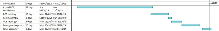
Here was my timeline when I sent in my boards. Some wiggle room incase anything goes wrong or I need to re-print any individual boards. It would be fine…
Original timeline
New Timeline
I uploaded my boards and sent the sales rep the images of the panel. And we messaged back and forth on Monday and Tuesday, she was great, clarified some of the aspects and checked that everything would work out. Perfect 10/10 service.
Then a big typhon hit china and the sales rep told me everything would be delayed, and I’m yeah, of course, stay safe. I don’t want them to work while the weather is dangerous. Just some bad luck. Then on Thursday, the engineering rep came to me, and asked about some details that I had already messaged the sales rep about… I messaged the engineering rep back, but heared nothing.
At the same time as I went to order the parts, I realized several of the components I had planned for were out of stock. Some would arrive on digikey or mouser in the coming days. But one of them would not arrive till November. And I’m just… shit… But then I figured out that there was a sister components with just a slightly different footprint which would arrive just a week later. I could technically fit the sister component in the footprint I had. But as PCBWay hadn’t even started on the panel yet. I figured I could try for a quick revision, making a footprint which would fit both component versions.
Digikey:
Mouser:
Digikey Different footprint
My current footprint with the new component over it.
Old footprint
New dual footprint:
So on Friday, not having heard anything since I answered them on Thursday, I send a follow up message, and include the pcb revisions, and ask if they have not started on the panel yet, if they can use the updated versions. I hear back and they say sure.
Then come Monday after some more questions, the send back the panel files as I had asked for them. I check them and see this
I wanted the supports in white to be removed. No supports inside the red boxes. And outlined the breaking order I had planned for to make the boards easy to separate.
And I felt unsure if the ThunderKILL would like having a support there, and I felt the ThunderKILL would be more likely to snap than the break tab. Along with that they added an extra support all the way on the left, making it impossible to separate out the two boards. So, I messaged them back, asking if they could change it. They said they would remove the support on the left, but they still wanted a support on the ThunderKILL and suggested moving the support here.
However they still really wanted some supports here
And me being stressed, already a week late, said sure, go ahead. I could just sand down the edges if they interfered with the Wii.
Then… came golden week. A holiday where the factories were closed for the rest of the week… Just my luck. I had hoped to get the boards through before then, but they had not even started manufacturing, and they said the panel would take 8 days… My buffer time was shrinking, but it would still be fine…
Monday the week after, 2 weeks after I ordered, they started manufacturing. And they finished the boards by Saturday, so they were faster than they had said. So, I thought great, there is 4 days shipping, if they ship on Monday I will get the board’s around 16th, and I’ll have 2 weeks to put everything together. It will be tight, but doable. Though there is no longer any buffer for ordering new parts of re-prints if anything is wrong.
Come Monday, and I get a message saying, “Hey our system says you zip code is going to X-town, but you have put it as going to Y-city, please double check the address” … X-town is a district in Y-city. If you know London, Canning Town is part of London, though I don’t live in London. I message them back 30 min later, saying no it is correct, X-town is just a district in Y-city. And I keep hoping that they will still send it out with the shipment… Many hours later I get a “Ok, we will send it out asap”… Tuesday nothing… Wednesday I get a message that the shipping label has been made… Thursday nothing… Friday I message them, asking if there is anything they can do to get it to move, as it has been stuck for the whole week. And they say they will do some calls. Saturday nothing… Late Monday I finally get the notification that the shipment has been picked up… A week after it was done… And that it will arrive on Thursday the 23rd… That gives me 8 days to solder all the components, do final fitting, update and flash the MCUs, connect everything together and mount it on the Wii, print and assemble the final case. And anything else I need to do. No time for any errors, or anything to go wrong…
Now I have gotten that the PCBs would arrive today, a day early, so that is something. But with my current plan I think I’ll get rid of all the unnecessary things, like sleeping and eating, to get it done in time. Here is my new revised plan.
Wish me luck, I’m gonna need it if I’m gonna have any chance at all XP
(Got distracted and didn’t posted this when I intended, lol) Tuesday 21st (11 days remaining):
Worked on the Fujiflex and nand flex, not done, but the nand and the FPGA have been soldered.
Wednesday 22nd (10 days remaining):
Excited boards arrived, I studied them and de-paneled them. Prepared workspace. Then sanded down the Wii further to size.
Thursday 23rd (9 days remaining):
Desoldered components from the OLED driver board, and started on the RainbowBRIDGE. Only to discover I messed up… I had calculated the footprint for the RTD wrong. The chip on the driverboard uses a different package than the standard in the datasheet, so I measured it and generated a version in kicad. However I messed up the pin pitch and my footprint has a pin pitch ever so slightly smaller than it should be… So I spent the day desoldering the RTD, trying to clean the solder off it, then adjusting the pins to fit the footprint, and then soldering it back on. It is a mess and uncomplete. Had the boards arrived earlier then I could have done a emergency re-print with the right footprint, but with all the delays, trying to make the RTD fit is my only option.
QFP hell...
Friday 24th (8 days remaining):
I’m starting to feel a bit sick, probably all the stress, this competition, university work, and everything else… No matter, just got to power through, no time for breaks, I’m already so behind but I can see the end goal.
I start on the ThunderKILL, and god damn I underestimated the BGA components. I’ve done some BGA stuff with the PS3, trying to make a frankie, and some other PS3 projects, so I kept expecting the BGA size to be like the RSX… But yeah no… these components I’ve chosen are way way way way way way way way smaller, and the balls are just pin pricks. I spend a good amount of time fiddling with them, trying to get them soldered in correctly, but I have no clue if they are forming a good contact or not. And it is taking way longer than I expected. Yeah no, I feel my chances of succeeding slipping. I give myself a maybe 10% chance of having something which works as long as nothing else goes wrong.
Later picture of the ThunderKILL. Didn't take any picures in the half finished state. This components are hellishly small to work with... Especially bottom right, there is both a 3x3 and a 2x3 BGA chip both smaller than a 0402 capacitor.
Saturday 25th (7 days remaining):
I got sicker, I’m behind in college work, and didn’t have energy to work more on this.
Sunday 26th (6 days remaining):
Sick, no work, realizing I’ll probably not finish in time.
Monday 27th (5 days remaining):
Sick, no work.
Tuesday 28th (4 days remaining):
Got better, but got to catch up on college work. No work on the project.
Wednesday 29th (3 days remaining):
Finally, back at the project. Finished soldering the ThunderKILL, untested, unflashed. Also fully soldered MelonLORD, EastECHO and GhostPAW, all untested, unflashed.
I discovered while working on the EastECHO that DigiKey sent me an empty strip where I had expected the clock crystal for the MX chip so there will be no MX time functionality... yay…
What remains:
Finishing RainbowBRIDGE, NandFlex, FujiFlex.
Flashing all the MCUs and updating any firmware.
Finishing the case and doing final print
Connecting all boards together and to the Wii
Testing the console
Final assembly
Make video (haha as if I’ll do all above in time XP lol)
Probably other stuff I’m forgetting.
I’ll try to keep this updated for this last bit of a scramble. But most likely my revenge won’t come in time… But I’ll see how far I get before the deadline, then finish it properly later.
Thursday 30th (2 days remaining)
Did more work on the case, and did a print of the case on my 3d printer. Had planned to do the case in resin, but won’t have time. But I have a purple filament, and if it turns out decent, then I can do a last print tomorrow and fix any remaining issues.
Spent the rest of the day messing with the RainbowBRIDGE, trying to fix the RTD chip being the wrong footprint. God it is so finicky, but I think I got it in a good place in the end.
At the very end of the day the case is done printing, but don’t have time to test fit it.
Friday 31st (1 day remaining)
… Tried fitting the finished PCBs into the case… and the buttons won’t work… nor the d-pad. I got some super slim buttons that I thought would be an improvement on just having rubber domes. I had planned on having the pattern for rubber domes underneath but skipped adding it due to time pressure. And now the rubber domes don’t press down on the slim buttons I have, and they don’t add enough spring to the buttons to make them reset properly… So they feel terrible and won’t work.
At the same time as I tried assembling everything I managed to rip off the ribbon cable for one of the joy con joy sticks. So all I have is one joy stick and the shoulder buttons. Though on a positive side, the shoulder buttons feel amazing, nice firm clicky, they are prefect, so… that’s something.
Ripped flex cable...
With one day remaining I can’t do another reprint so I can’t fix the buttons, or get a new joystick. So think this is the end of the road.
…
…
…
A few hours later, I felt like trying to go a bit further, finish up the RainbowBRIDGE to see if it will work, then might solder the FujiFlex and ThunderKILL to the Wii and see if I can get it to boot. Even if I don’t have buttons, I might still have something bootable.
…
Worked on the RainbowBRIDGE aaaaaaaand I forgot to order the IC which handles power delivery to the OLED panel. So even if the scuffed RTD chip still works and I managed to get the footprint right, I can’t power it… And don’t have time to order the missing IC…
Left side upper middle. Also yeah I know it is crusty, I tried to clean flux with IPA, but think even with 99.9% it is leaving a residue around the components.
Some more work, added the connector on the back for the RainbowBRIDGE where it is supposed to connect to the display… And I got the wrong connector. I had been unsure about it from the start, and it was on the list of things I wanted to check in case I needed to reprint… But yeah… no reprints on me.
These connectors don't match...
And just to put a nail in the coffin, my hot air station started making a popping sound, with the air pressure shooting through the roof with every pop. It sounds like an air pop, so might be a seal or something broken, but it means no more hot air, can’t finish the FujiFlex, so I cant test the video out of the Wii. At this point there is no point trying to assemble it any further.
Final comments/submission
The RainbowBRIDGE is triple broked, so no display for me. Buttons are nonfunctional, so I could not interact even if I used a external display. One joystick is dead. I don’t have Z button as I never added it to the case. My hot air station is borked so I can’t finish soldering. Oh, and yeah, I forgot about the height of the minijack for the external GC controller, so my cooling fan won’t fit where it is supposed to. So yeah… this project is not coming together for this deadline. Think I’m gonna leave it here, call it done, and move onto my next project. Might try for a reprint during Christmas or something, to see if I get it working in the end. But yeah, luck and revenge was not on my side this year.
But I have learned a lot, among them plan more time for pcb printing, and more spare components. For next year I have a even more ambitious project planned, so I’m looking forward to that, a V4 will come, even better and hopefully maybe even perhaps possibly working, who knows.


")