- Joined
- Jul 9, 2020
- Messages
- 230
- Likes
- 500
Hey y'all... been putting together an Ashida build and its been really fun. A few speed bumps and road blocks but I'm loving it. It's not going as smoothly as I had hoped... so its about time I update a work log to see if I can iron this all out. ")
I ordered the PCBs on day one and soldered all the parts on as soon as they came in the mail. I still didn't have a case though. I took the internal buttons and pads from an official gamecube controller. Got the good stick boxes with the screw mounts. Nice! Mounted all the switches and opted for ribbon cable. I don't think took any pictures of this stage.
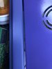
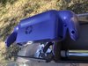
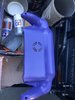
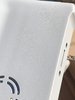
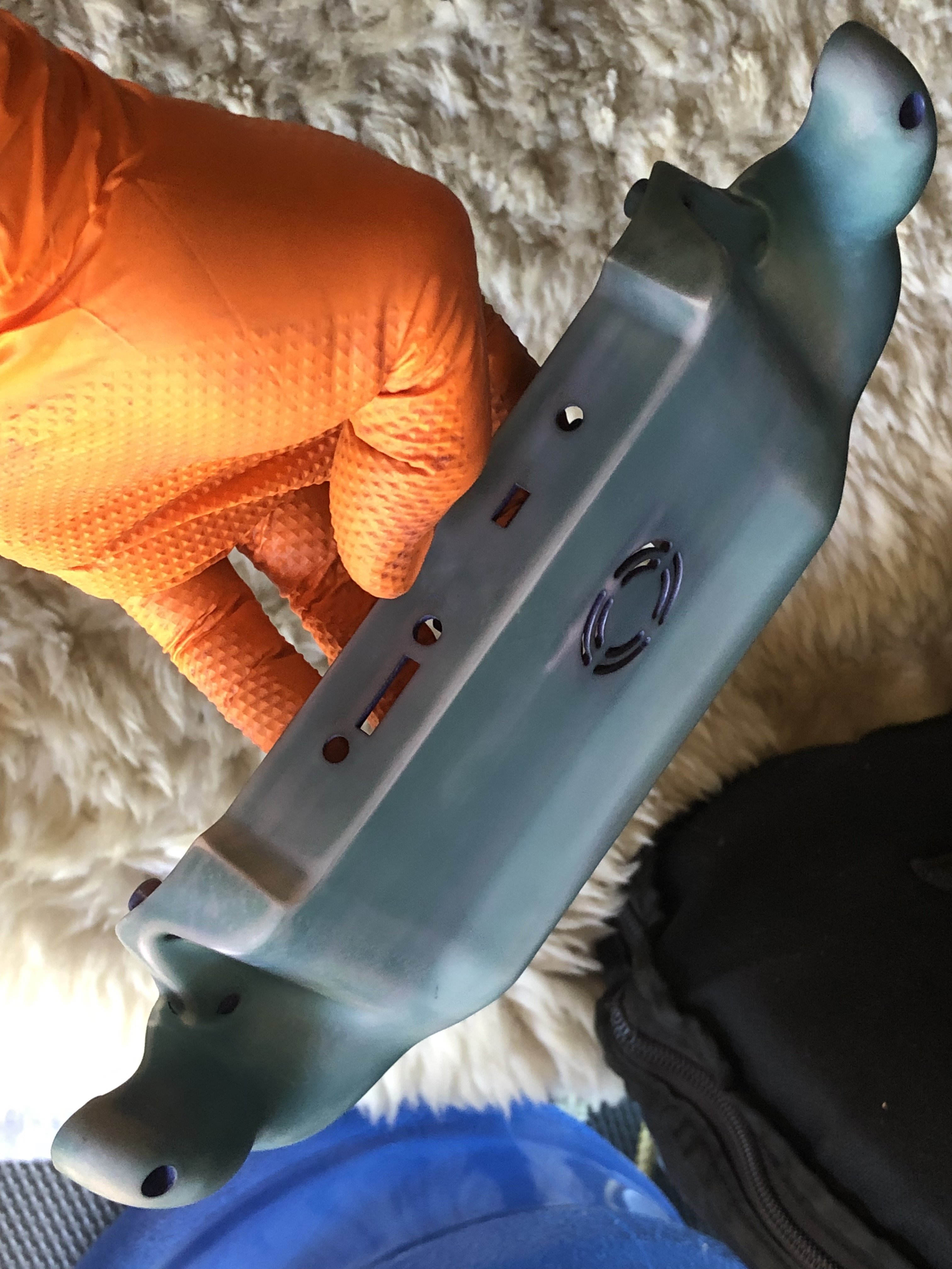
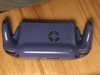
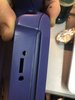
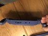
A few days after the Ashida was released, I ordered UTR 3100 dyed indigo from PCBWay. The case that arrived was painted as some of you may know the story of my and @Shank 's cases. They were not able to do a good dye job so they just ended up spray painting it.
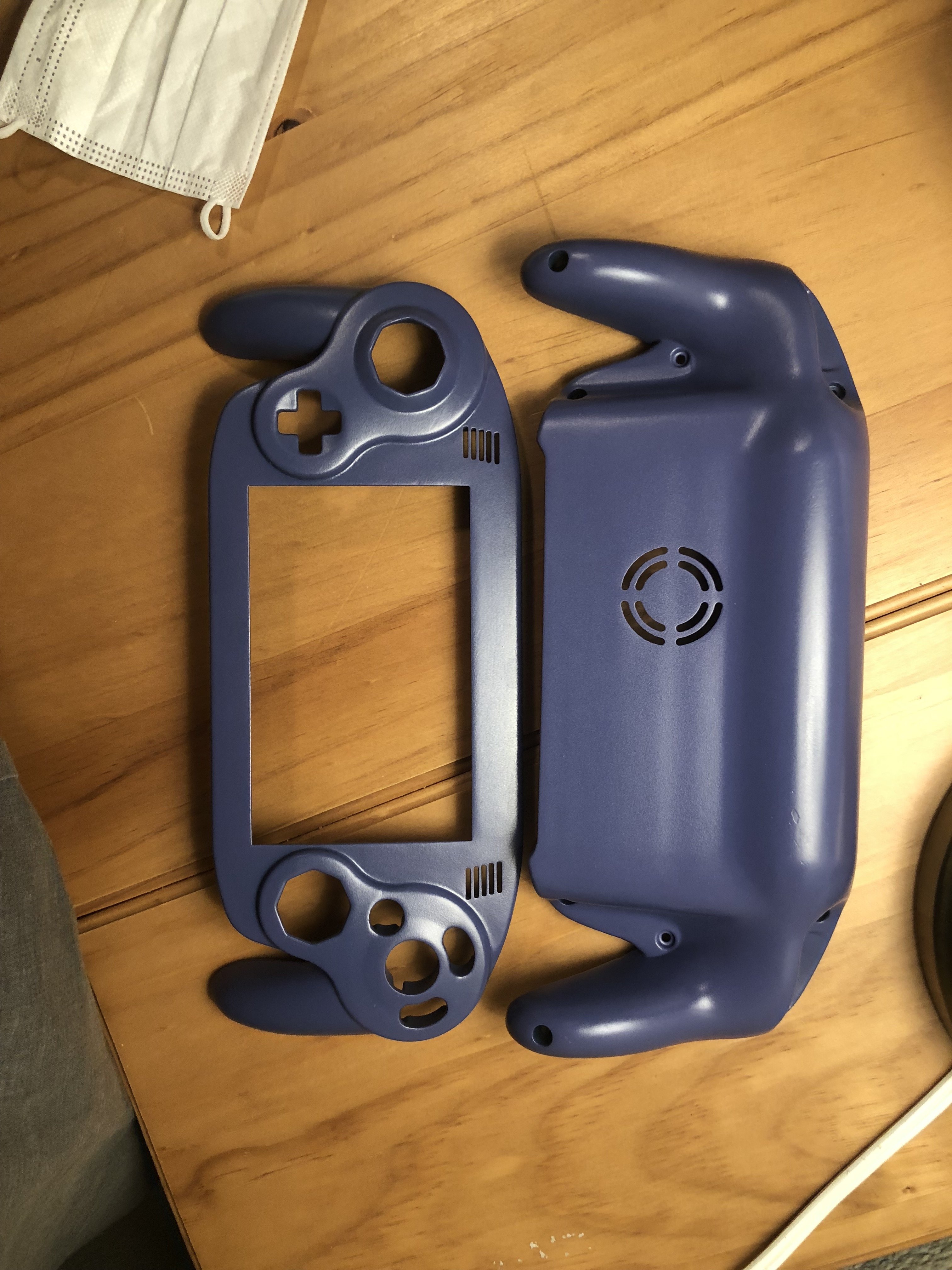
I was not totally happy with the paint job. Gman had given advice about going lightly and slowly with 1500 grit wet sanding to smooth it out and apply a clear coat. I thought it would be a nice thing so I decided to try to do follow that tip. I had never done any of that before so I kind of took off some of the corner paint. The layer was incredibly thin... woops.
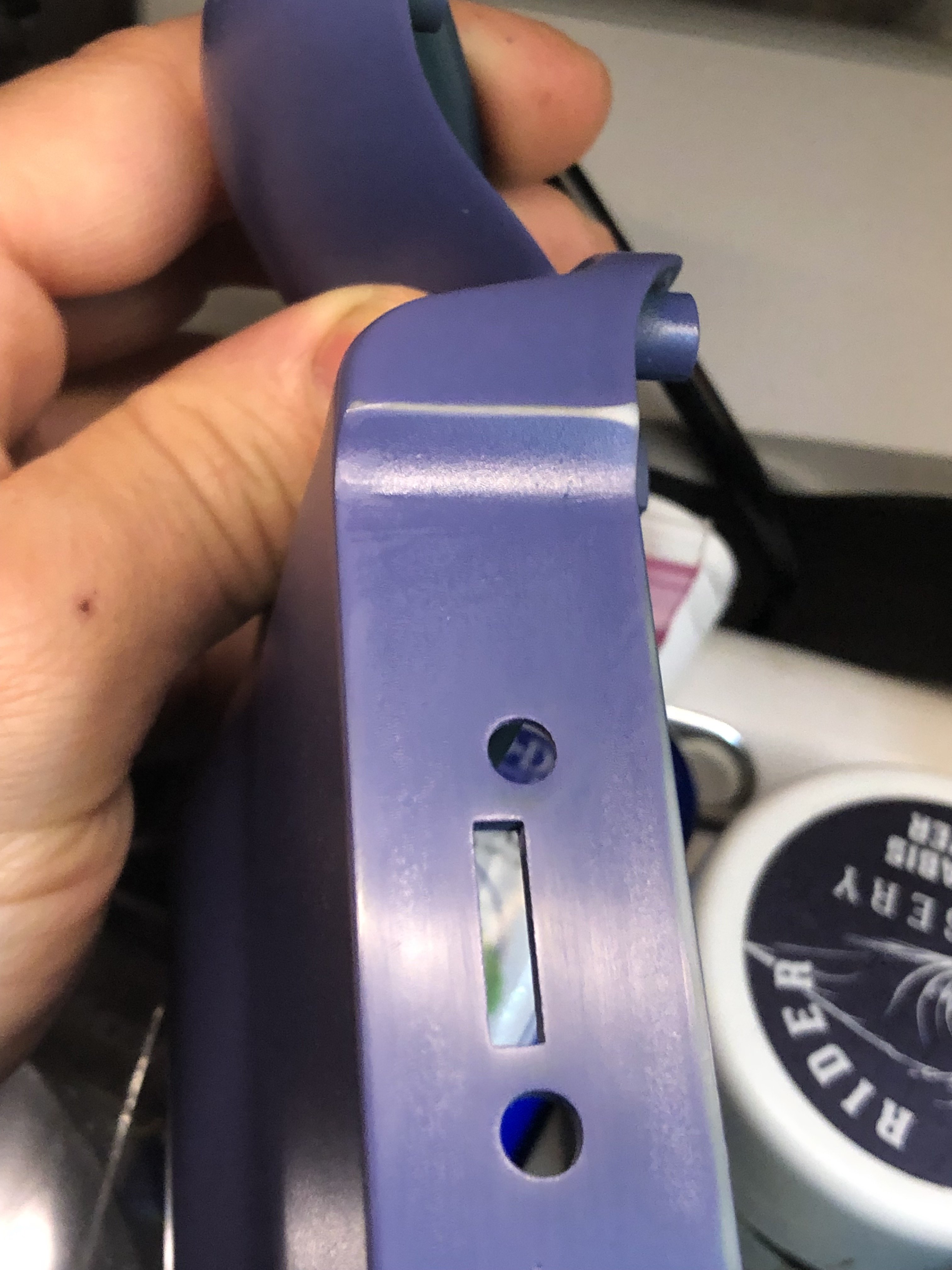
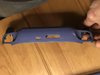
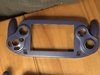
Then, I accidentally smudged the paint with IPA after cleaning a pcb. double woops... This prompted me to just strip all the paint off in hopes of repainting it nicely one day. I used 99% ipa and a clean lint free rag to rub off the paint layers. It has a strange appeal to it... Like a vintaged fender guitar. Except the partially dyed color is only OK looking. In retrospect, the paint job was actually not awful... Learning experiences.
I ordered some paint for the back, but actually couldn't wait any longer to build... so I just went with it. Whatever, it is what it is...
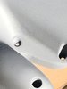
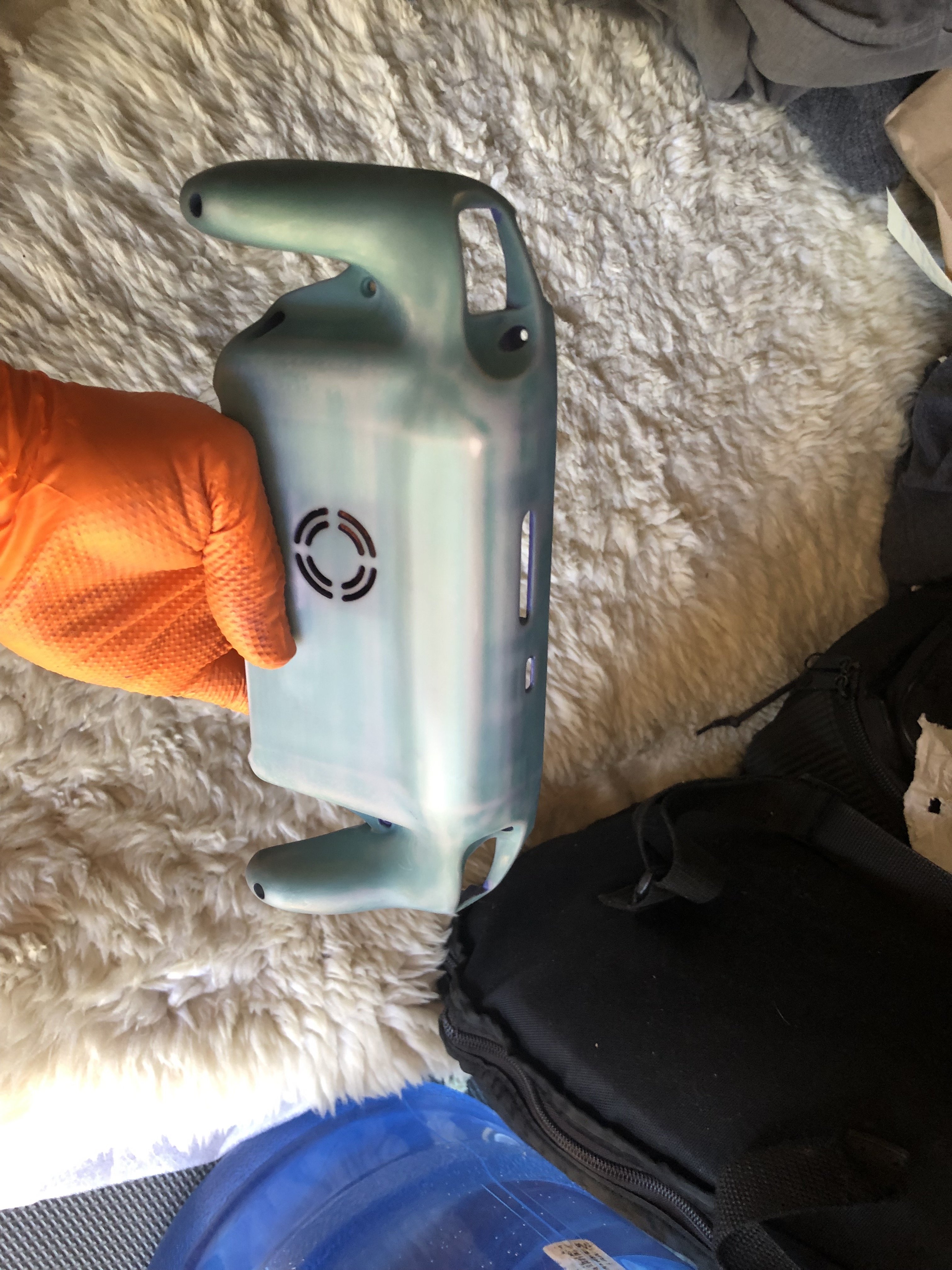
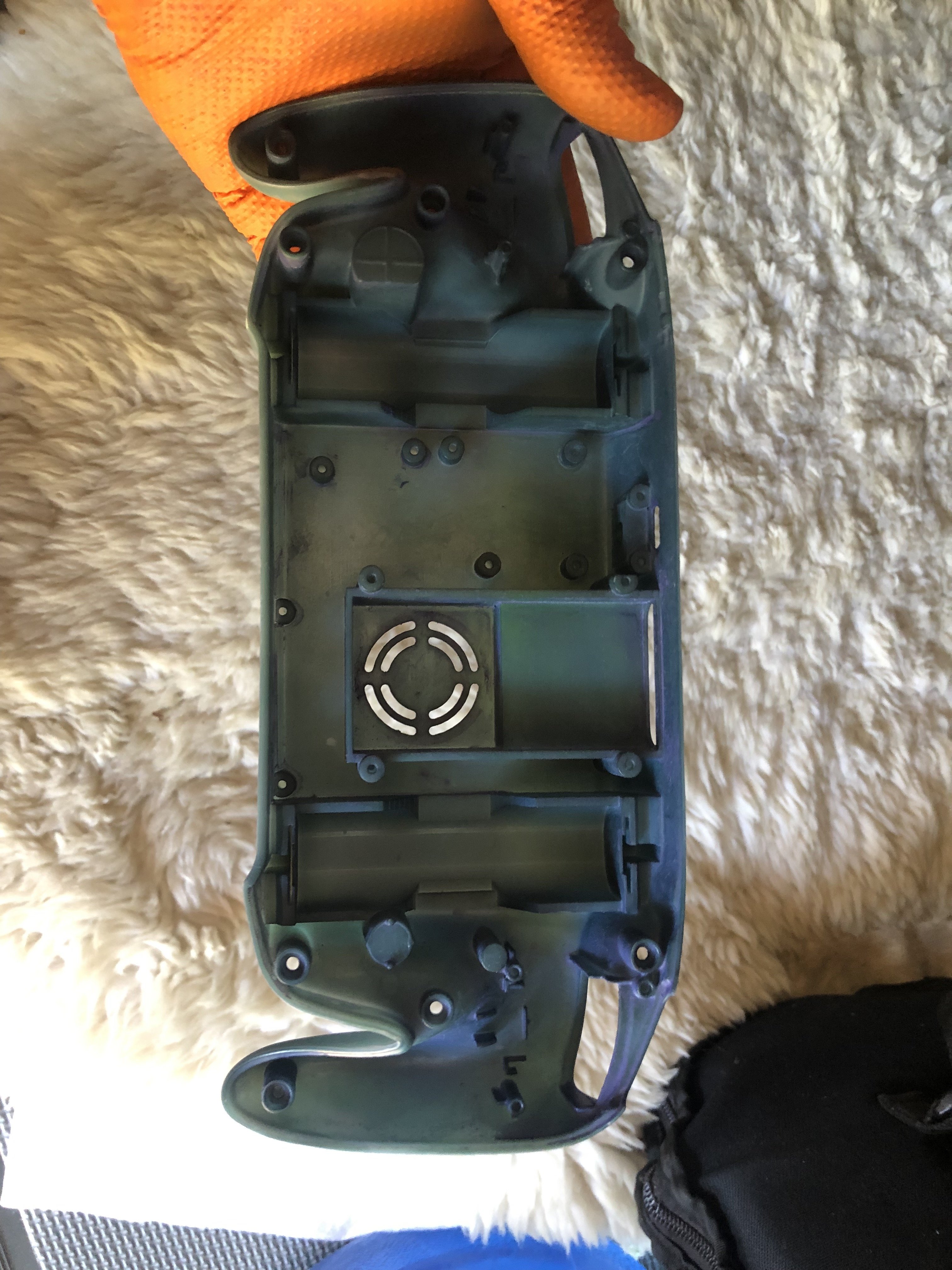
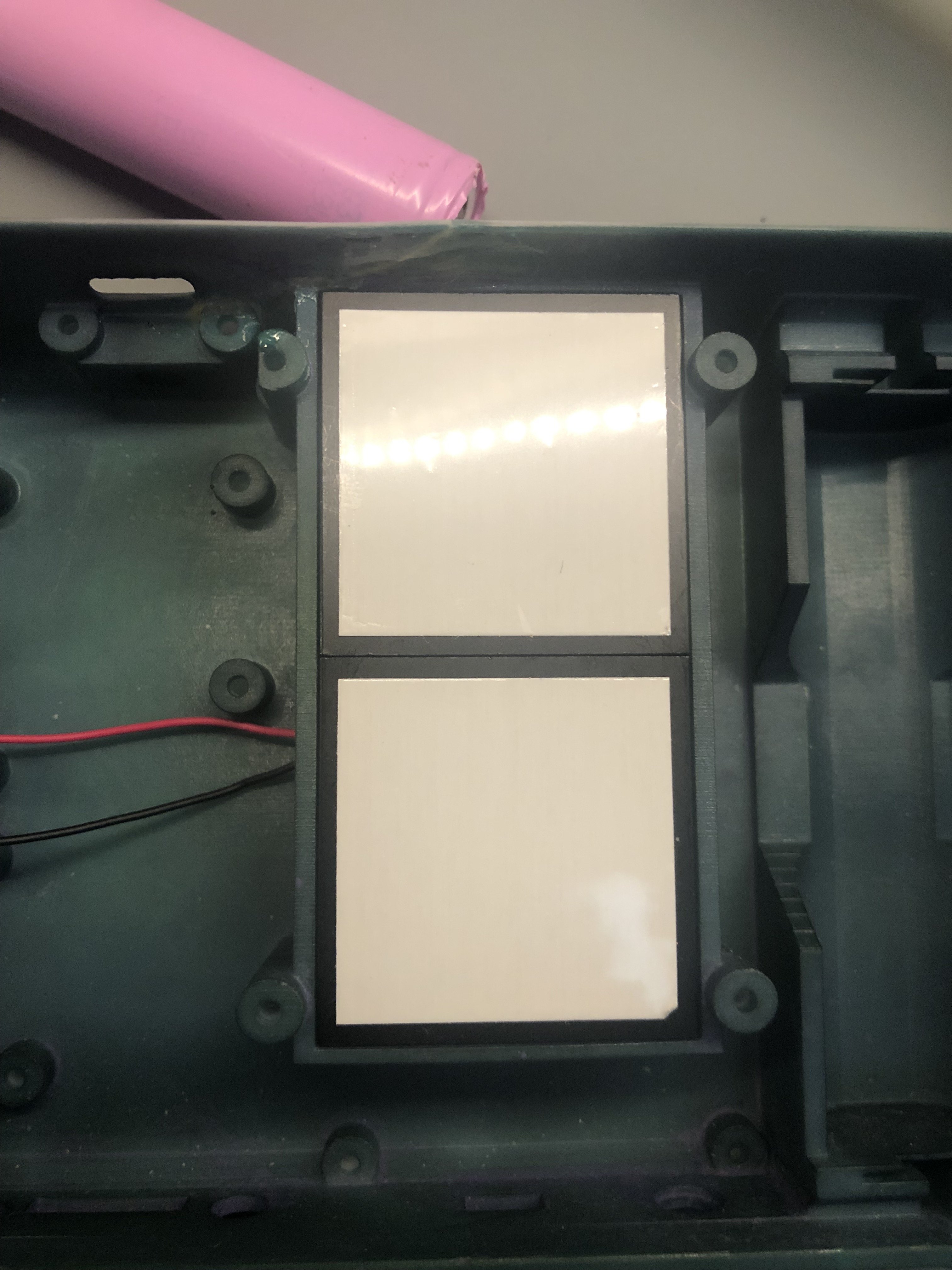
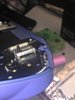
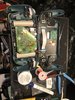
I started on the cooling system... Stuck the fan in with the sticker facing out so the axial fan sucks air in rather than pushing air out through the adjacent fan hole. There is a slot where the wires will pass through unhindered so they can be wired to the PMS. Inserted the two heat sink so that their channel was aligned with the exaust port on the top of the rear case half. Placed in heatsink with fins facing the fan. Prepped a piece of copper that was just big enough to be effective from a scrap I had in my parts bin. Peeled off the adhesive on the heatsink and stuck down the copper.
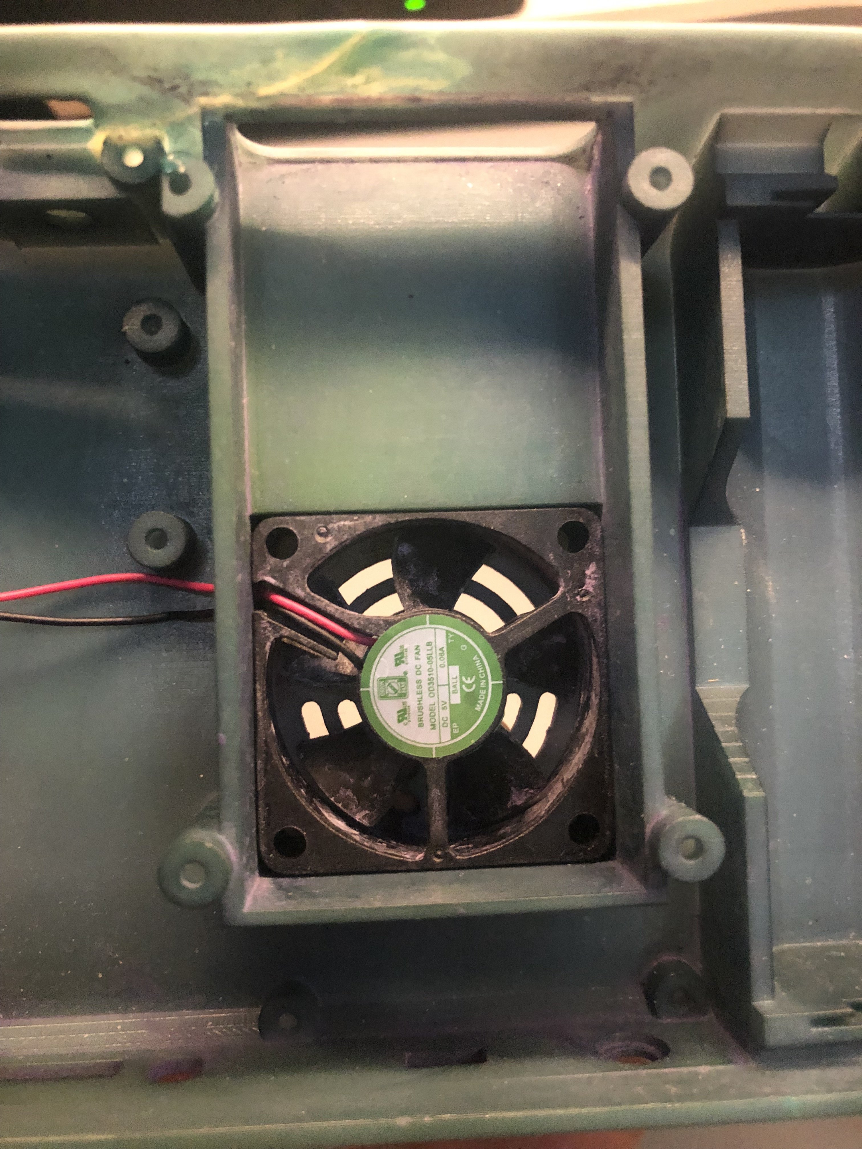
(i also accidentally left the fan in the rear case in the first few minutes of wet sanding hence the paint stains and loud bearing... ill replace that woopsie one day soon)
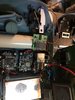
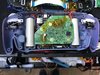
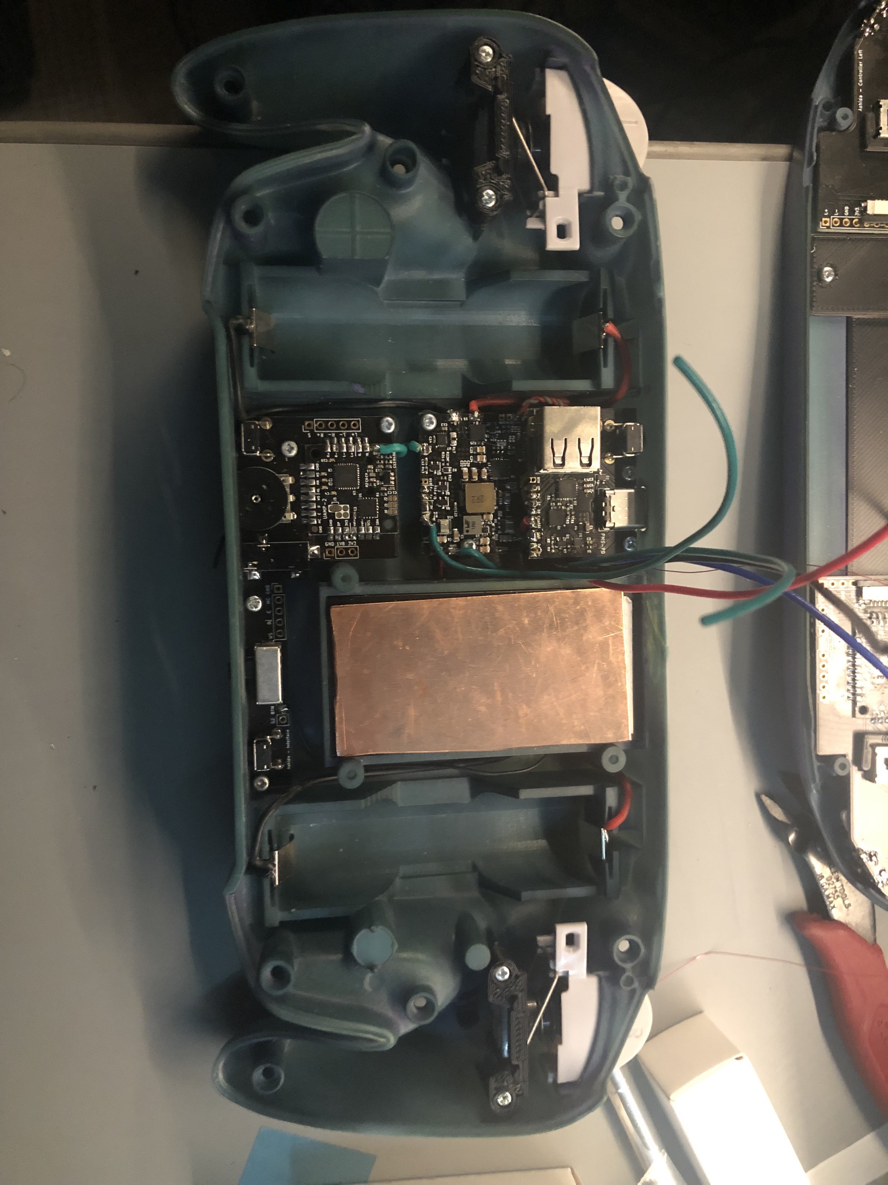
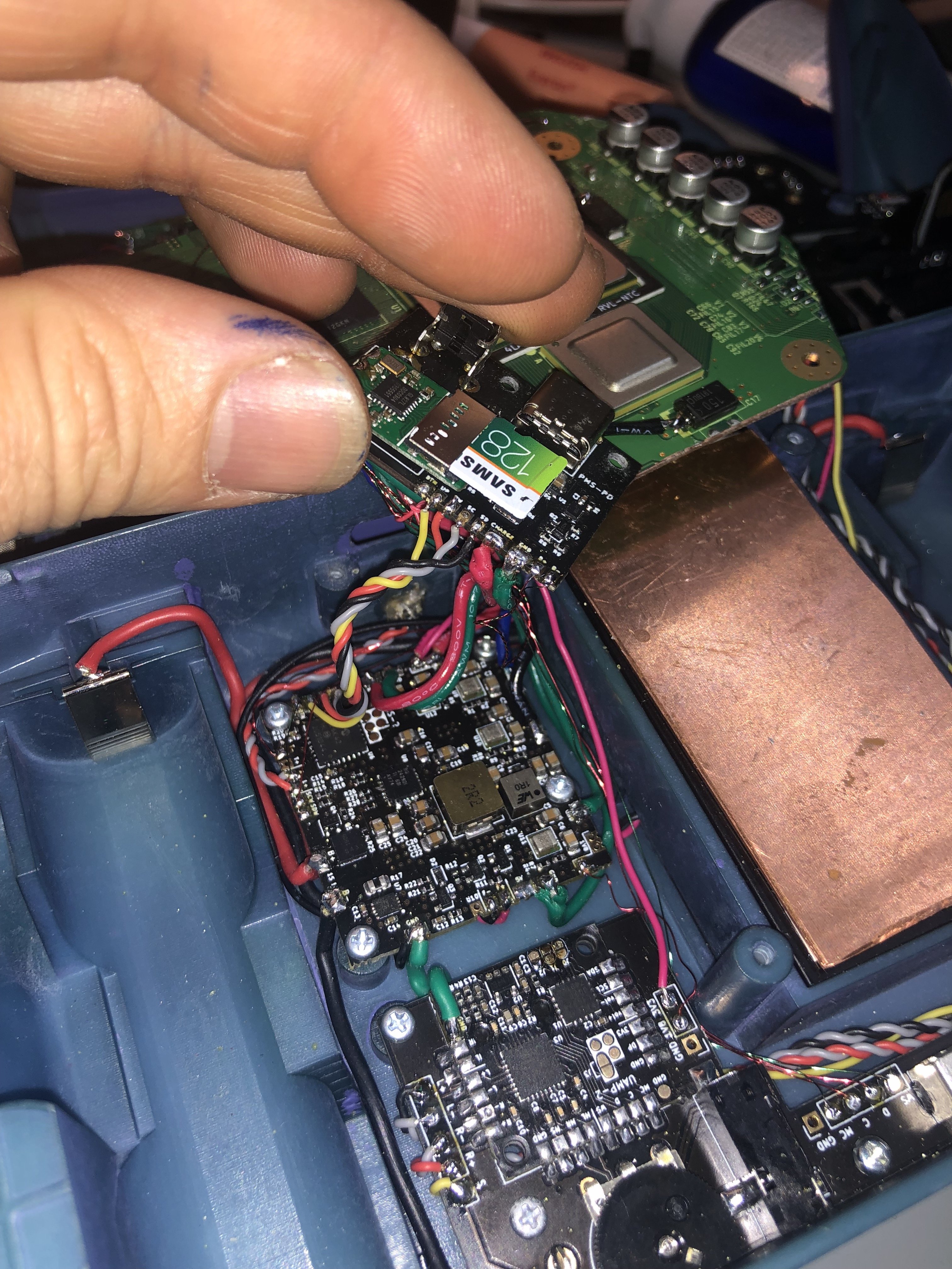
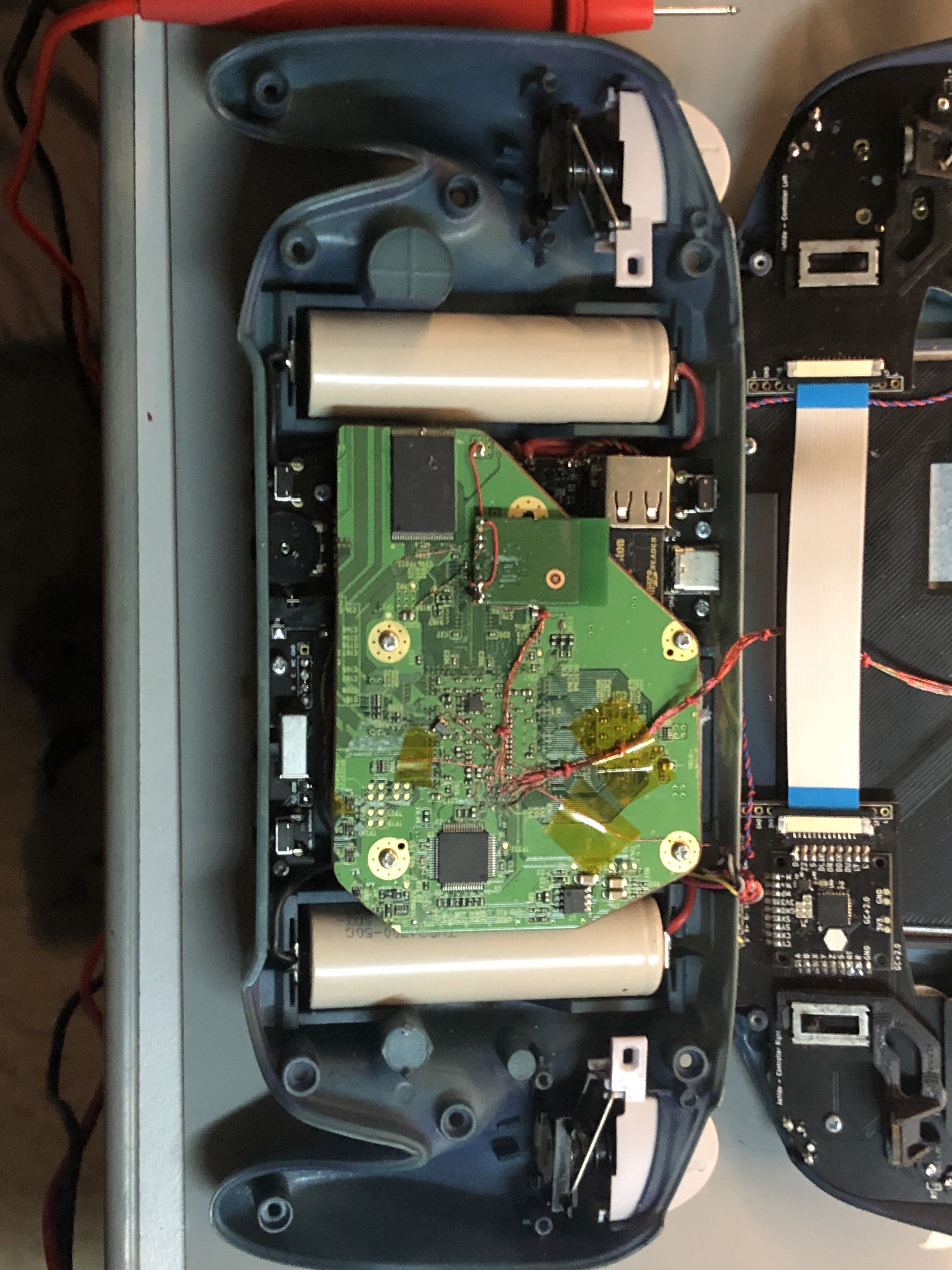
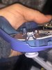
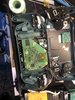
Wired up my PMS2 and PMSPD, dropped in the populated Ashida custom PCBs, wired up grounds, battery clips out in shoulder button assembly.
Put leads on voltage lines with color code. One thing I found helpful with the battery clips was not to solder the wires anywhere but the top edge so that the clip could fully seat in the slot. I also ended up running battery wiring through the handy pass through that is a the same depth as the fan in that negative space in the back face of the rear case half. Great layout.
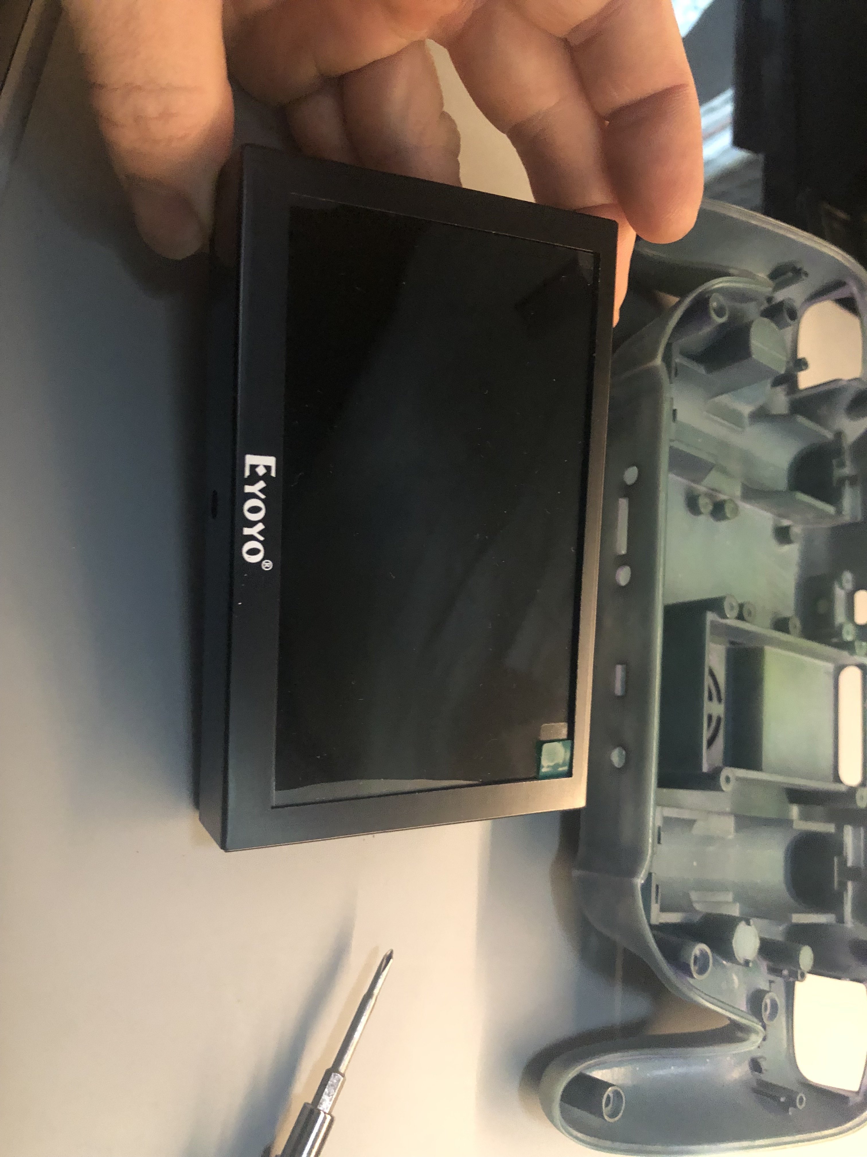
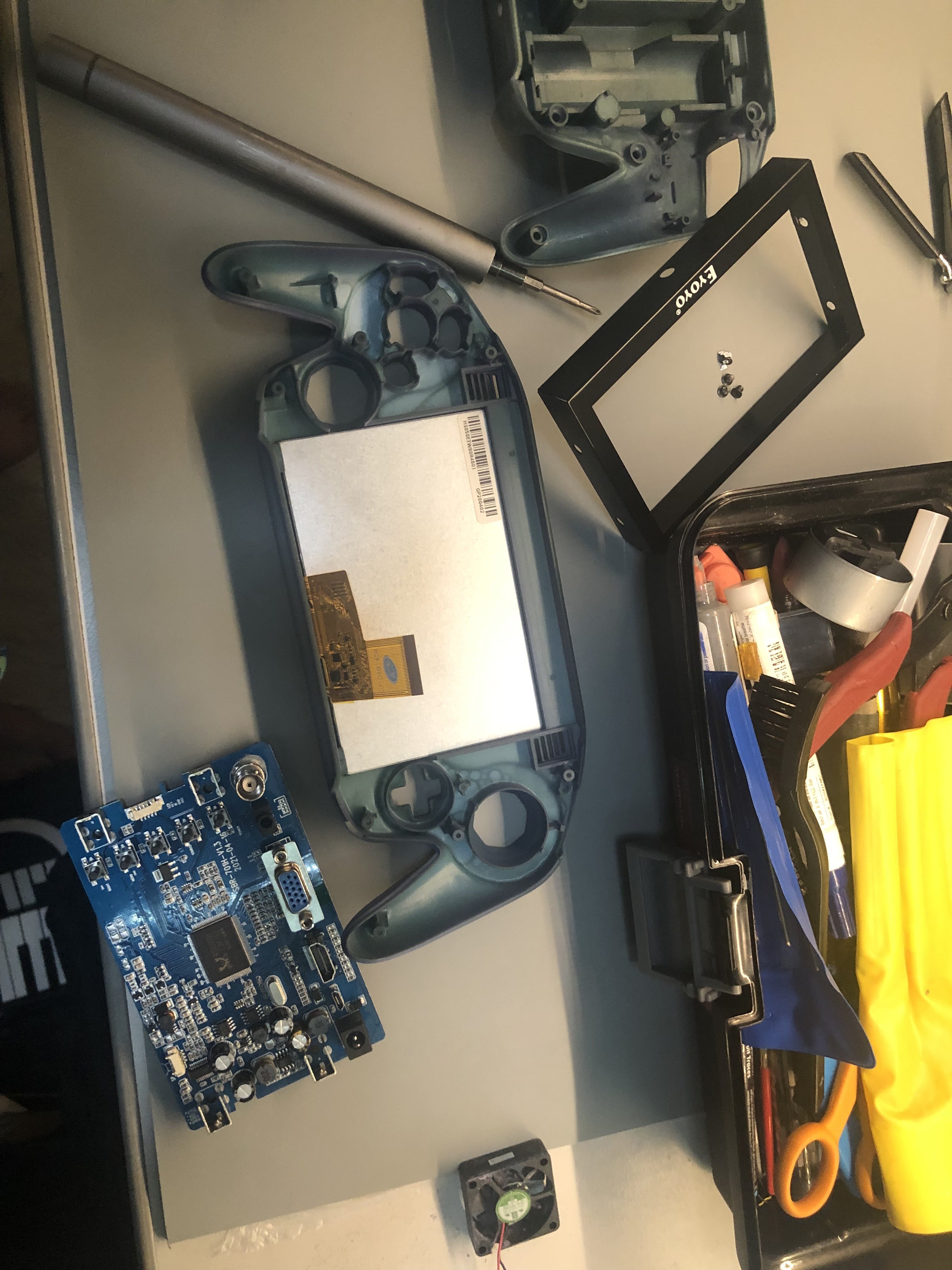
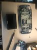
Disassembled the eyoyo ips screen case to discover a BEHEMOTH of a screen driver board that would never fit in the portable. Also, fit caps and buttons into the controller and boards... Its cool I didn't need to modify any buttons or pads for my build... @Wesk said you might need to with some pads but we are not sure. (You will have to modify the Z button plastic male hinge part... just trim/sand the longer nub a bit shorter so both sides are about the same nub size.)
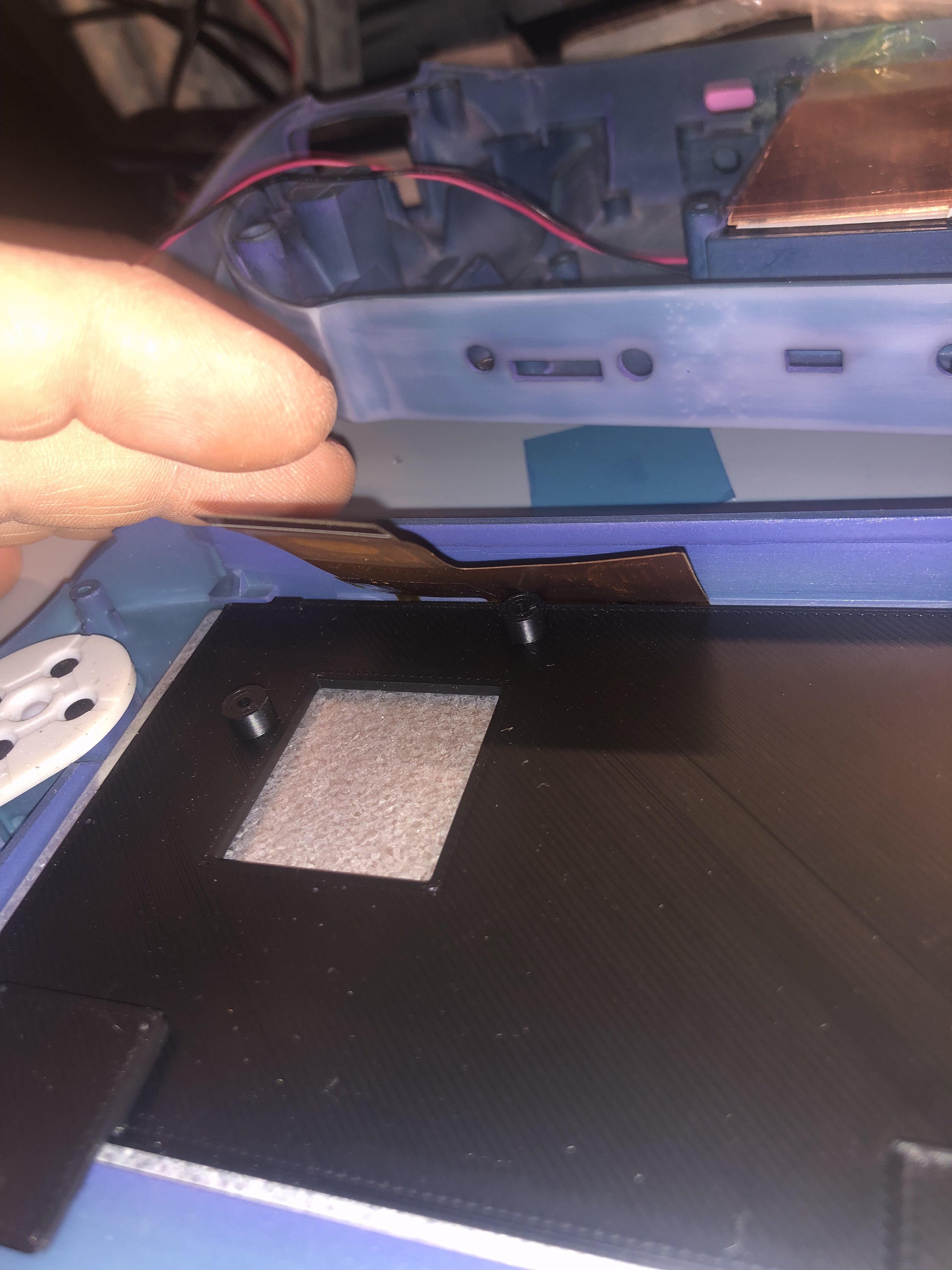
I hadn't planned on using my DirectDrive (DD) board for this project, but it was my only choice if i wanted to move forward with the parts i had on hand. Its a worthy project and a worthy screen. Set the screen in the slot like a glove... At first, I accidentally tried to attach the DD screen mount board with the ribbon set to go OVER the mount... but it actually goes flat against the screen with the mount on top of it... then bends around through the hole to mate with the board. Made a mistake about that at first... Never again. What a cute little board! Was so excited to see what it could do.
Oh, one note about the tact switches for the Z buttons... I didn't have the correct kind that matched the holes in the ashida board. Not sure if anyone was able to source these but I couldn't find them. I ended up just using regular short clicky tact switches, Cutting one side of the legs off and soldered them in place. Using solder, I carefully bridged the mechanical support pads to the front metal face of the tact... this will help support with the stress of pushing the buttons. Be frugal with the solder because it can flow into the plastic part and fuse it in place... this worked perfectly.
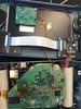
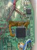
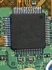
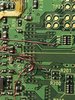
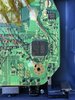
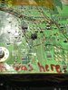
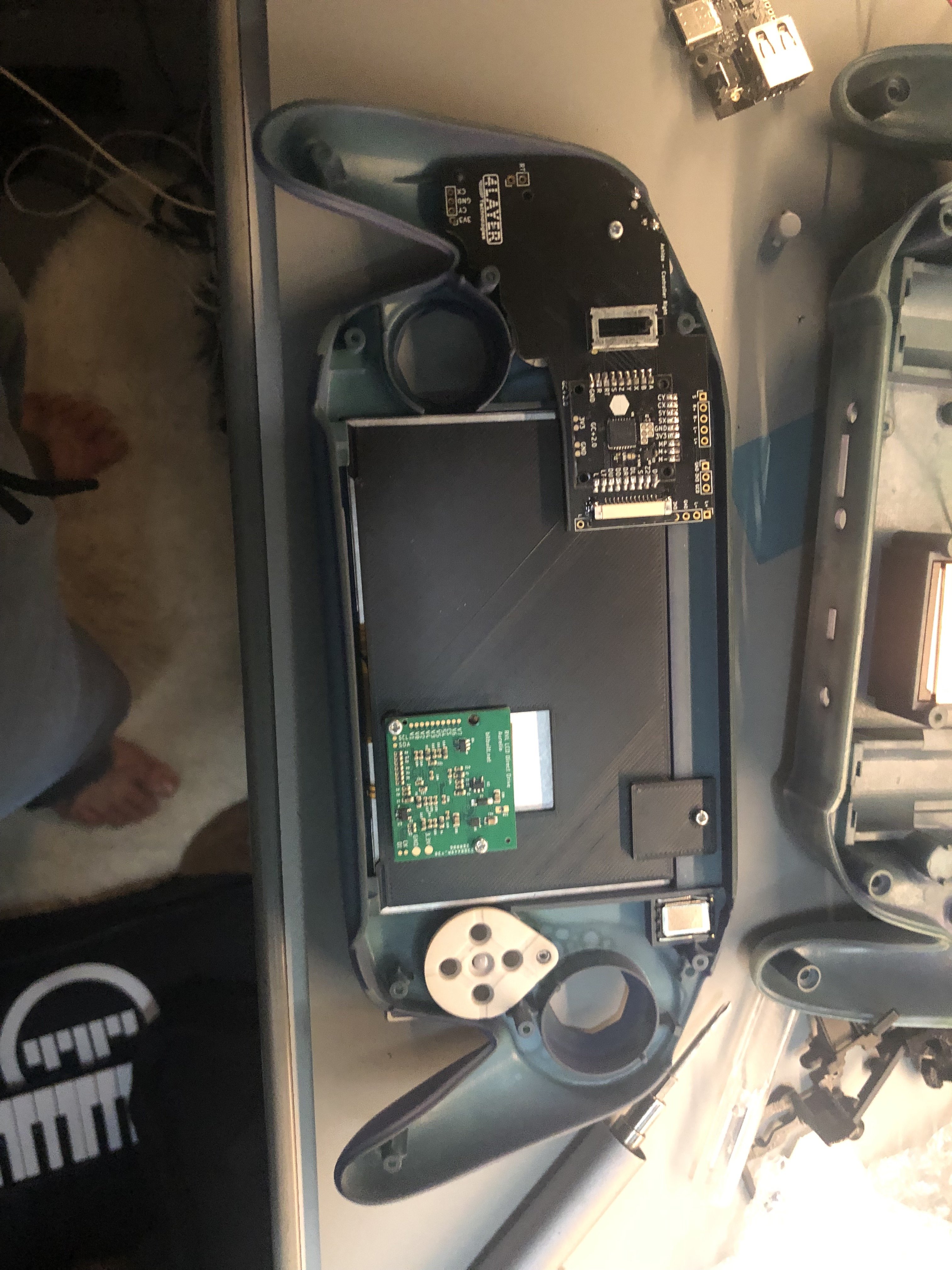
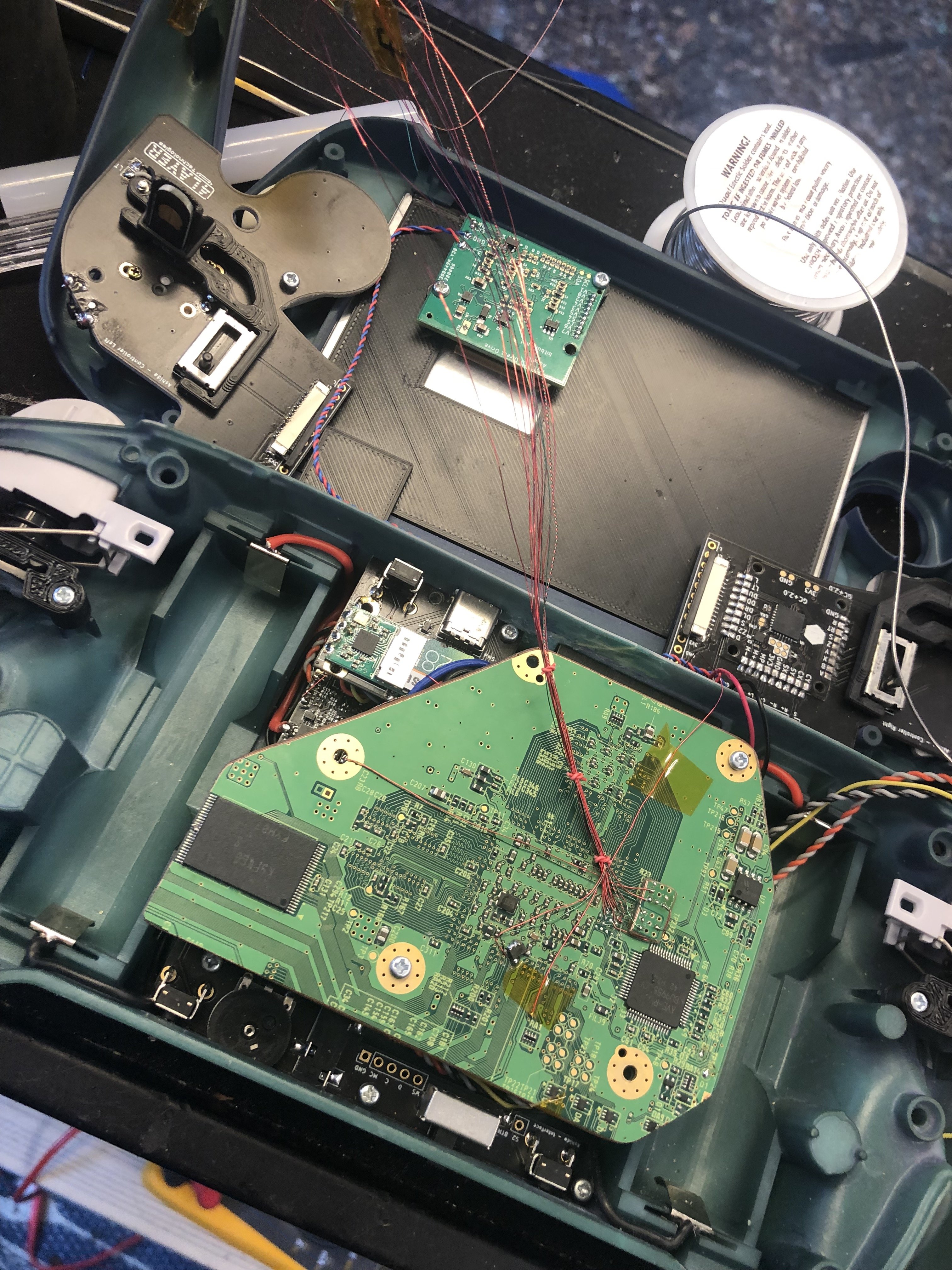
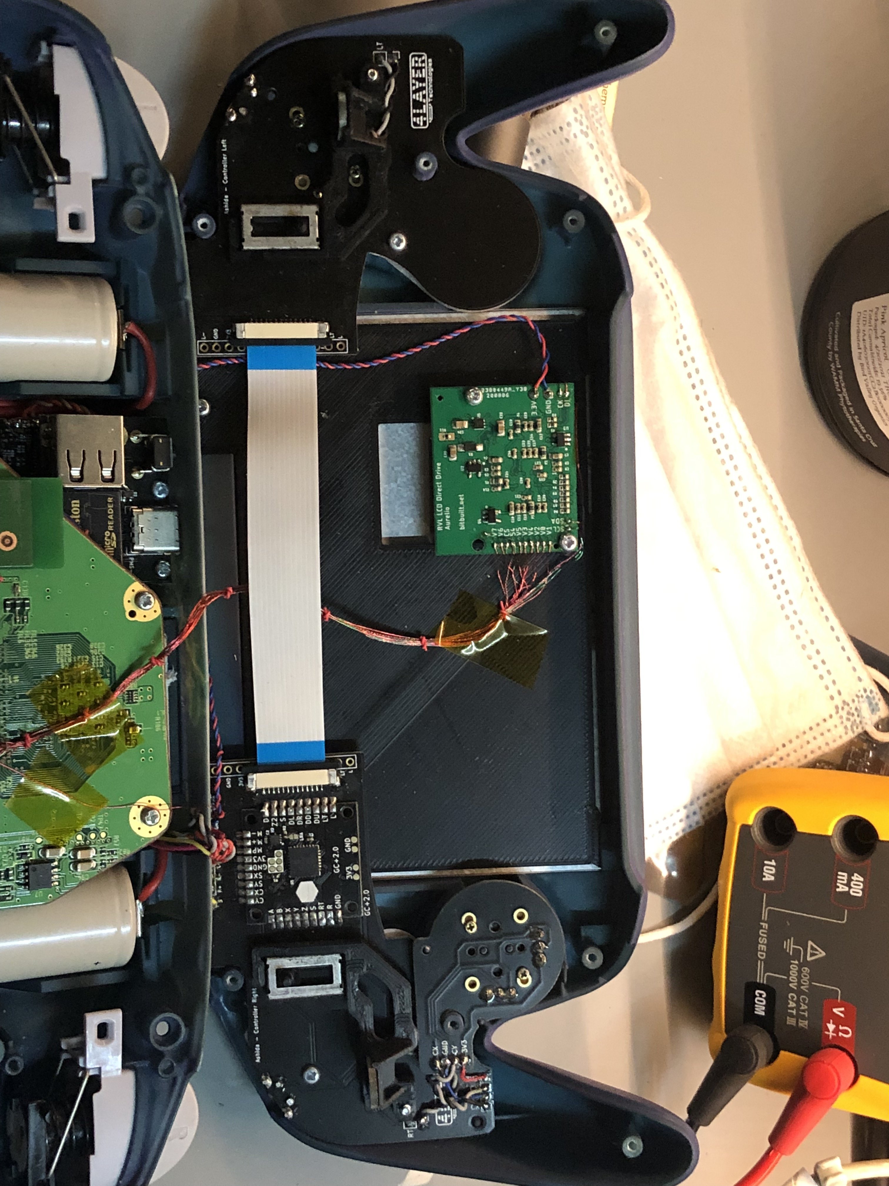
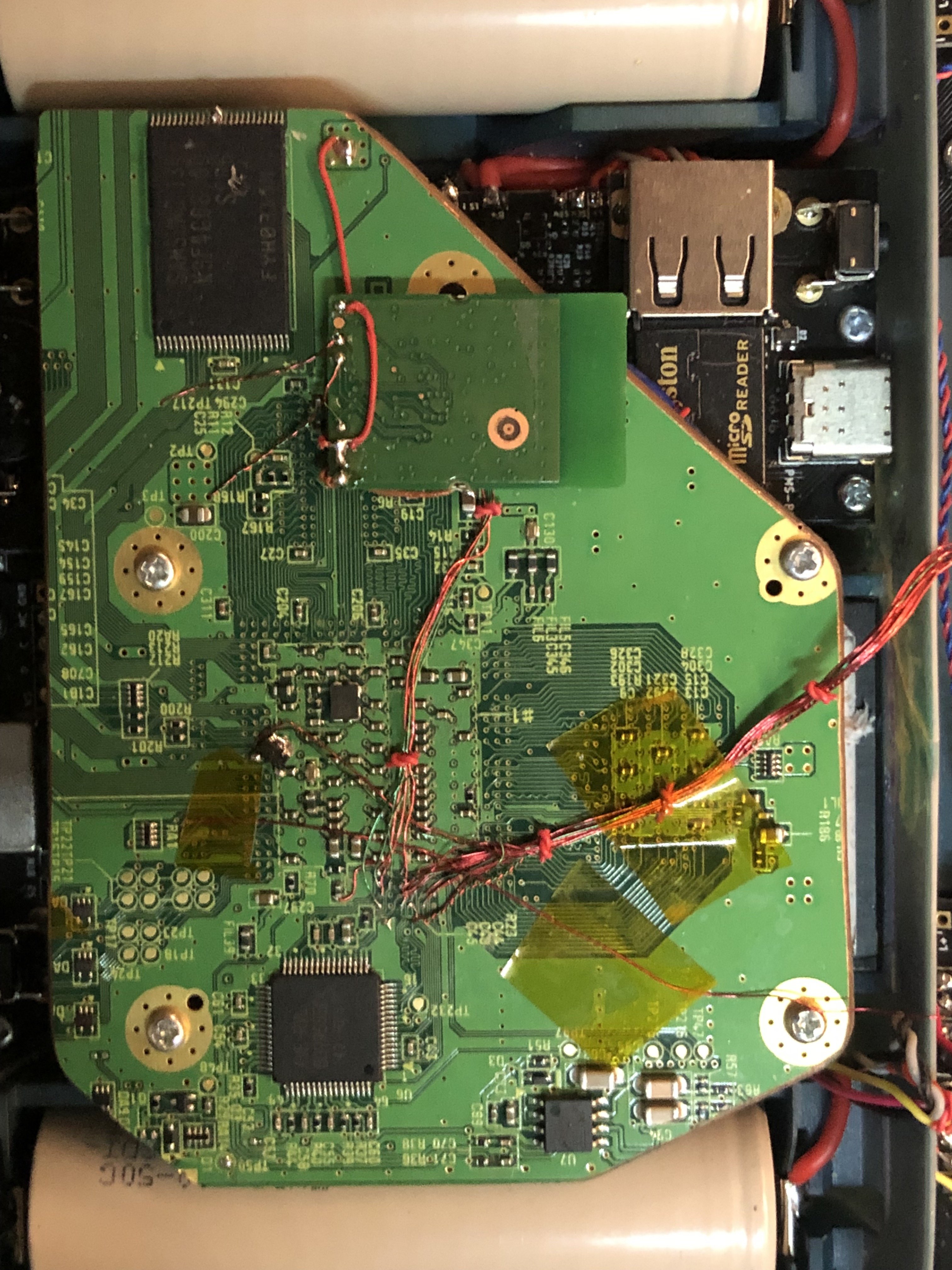
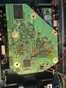
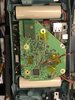
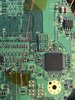
Time to do a quick trim and sand of a prepped 4 layer board... easy peasy. I've developed a trim method where after I cut the outline I will use the top face of the cutting wheel to sand the edges at a diagonal to get a good bit of the work done. Its kind of risky but i've had pretty flawless success with it so far. This time I actually got away with only doing a light filing with 200 grit diamond file and then finish with 320 sand paper. No shorts, all resistances were golden. I did the wireless U10 relocation and prepped all the i2c, DD and digital audio via's at the AVE-RVL patch points.
Wired up the Wii to the voltage lines... being sure to route them cleanly and cut them to length. Wired Power and Ground across the case halves to the GC+ board and jumped off of that for the DD power and ground lines. Soldered in the T- wire to the thermistor. Wired up the data lines... (of the two USB via sets, The INSIDE lines are D- and the OUTSIDE lines are D+... put that in the ol memory banks)... Ran the analog speaker wire pairs and start button tact line too. Wired up a temporary RCA cable to the composite AVE via and ground to test booting. Double checked there were no shorts... Popped the batteries in and pulled the switch...And it fired right up! Booting like normal...
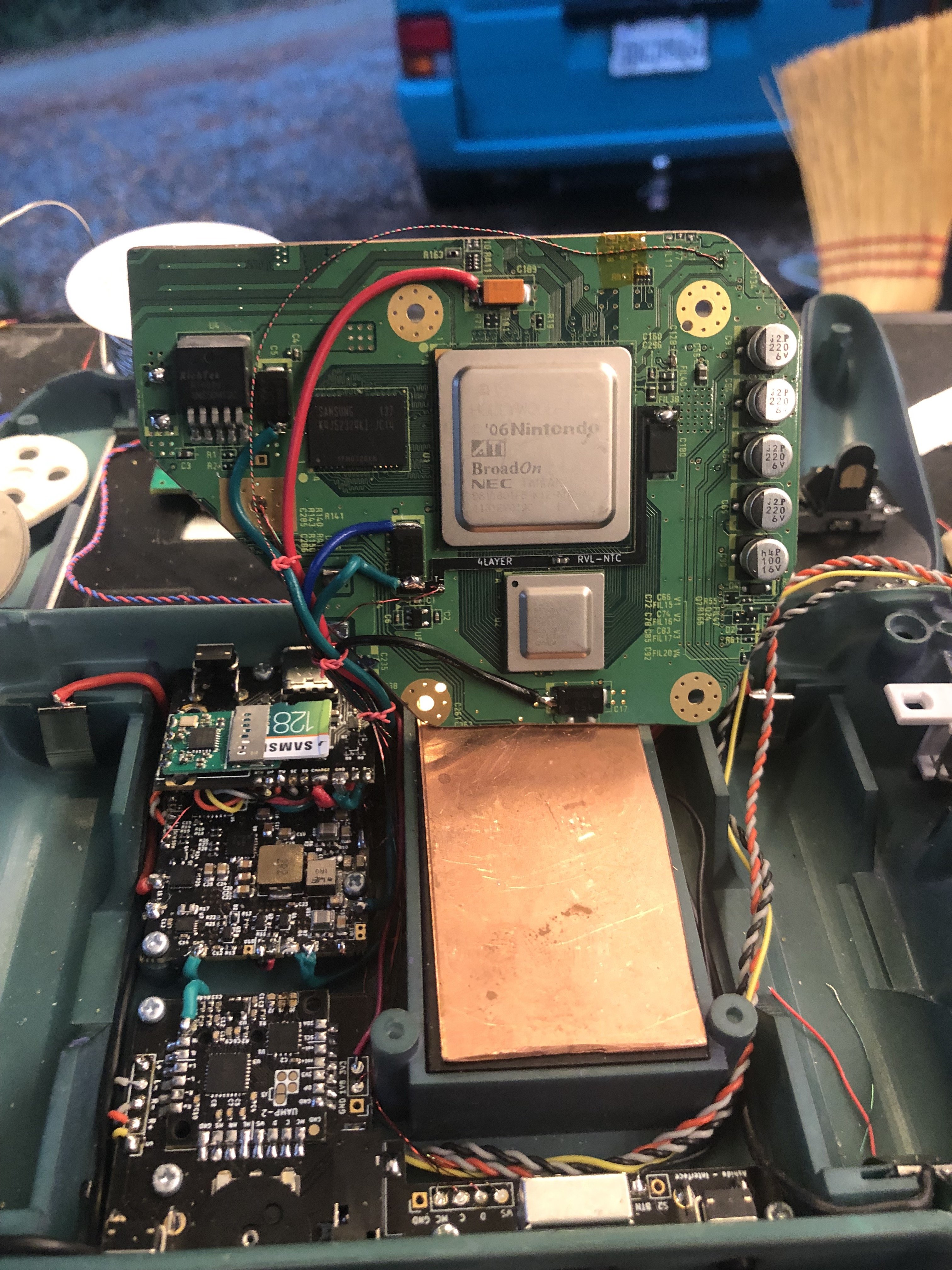
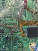
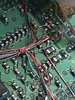
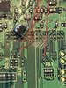
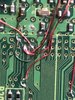
Carefully wired 34awg magnet wire to the via points for the DD and ran the labeled bare ends in the direction of the DD. I wanted to run all the lines and tie them off before wiring the other end so it would be a clean bundle. After tying them up I cleanly I cut each to length and soldered to appropriate pad. P1 data wired across top ready to go across the case to the GC+... I knew that i was going to have a few i2c devices that needed realestate at the vias. I tried one of these via fields that i trimmed off of the wii scraps. I thought I'd use one for SDW/SDA and one for SCW/SCL for PMS and DD i2c. However, this actually was the failure point. Maybe the extra layers caused interference?? I couldn't get them to work in the end but at this stage I was gonna try it. I also routed the digital audio wiring across and down to the wire run on the voltage side of the mobo.
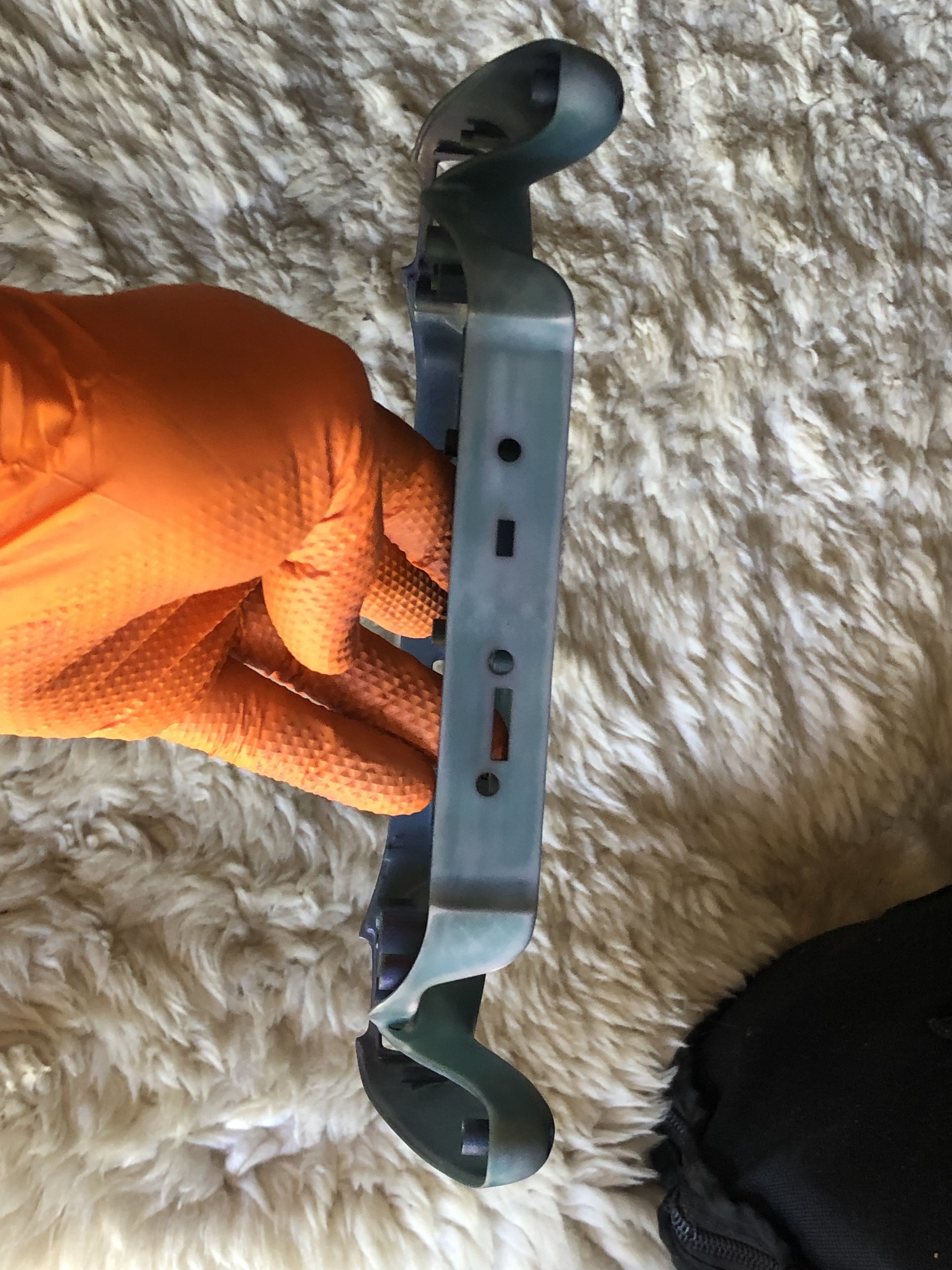
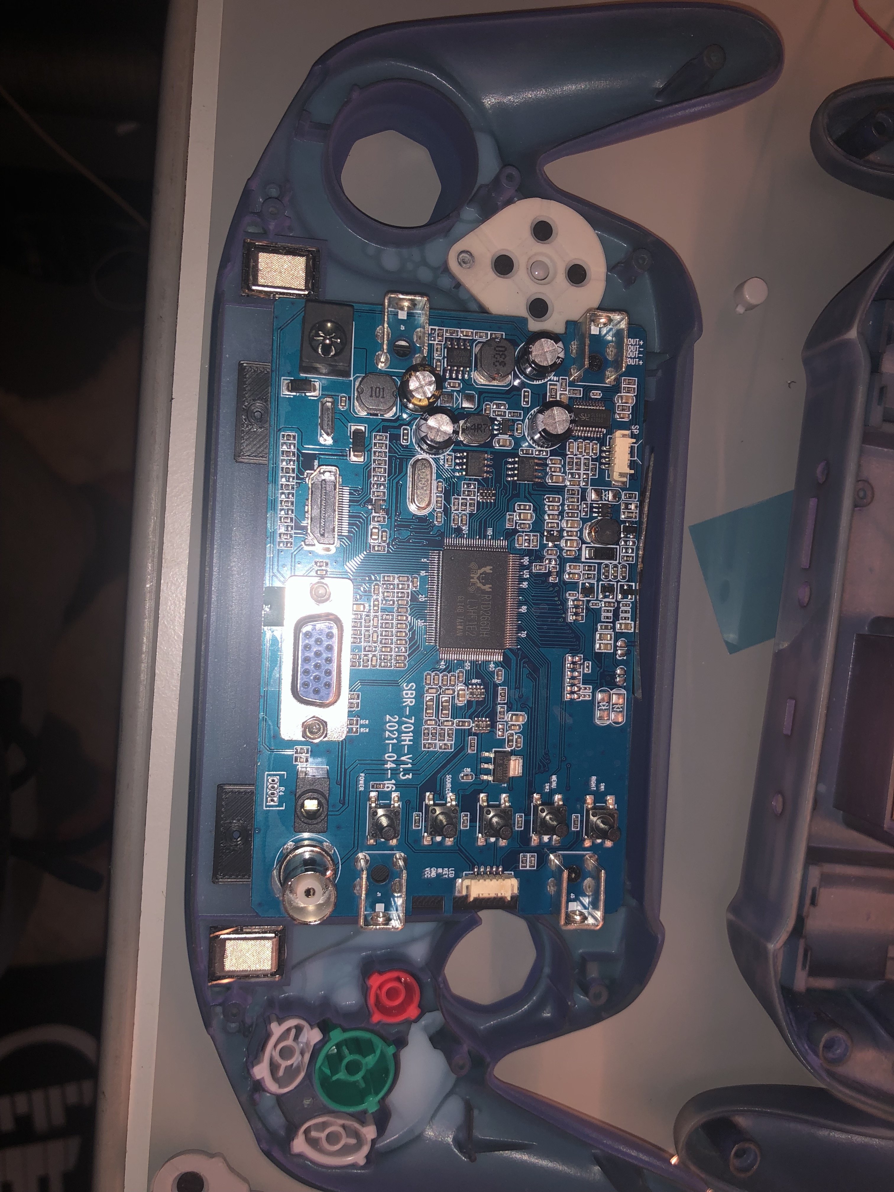
Also take note of the trigger brackets, this stumped me at first when wesk recommended I just watch the release video! It shows every part fitting together!
The first test of the DD and Eyoyo screen yielded a crisp and beautiful video signal... Feels good.
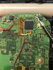
However, this is when I started to realize the problems. The PMSPD would not mount the SD card so i thought it needed a charge. The lithium battery I had came with very little charge. So, when I tried to test charging it led to the PMS board fritzing out and I think one of the chips got damaged... I have to inform y'all that the PMS board i used for this build at first was one of the boards i "fixed" from a short circuit mishap weeks earlier. I replaced the BQ chip and it booted up and voltages were outputting properly... I didn't test charging. So, something was wrong... And I believe this led to the PMSPD to also be damaged. I can not know for sure because my intimate knowledge of the deeper workings of these boards are still a bit beyond my understanding... but thats my hunch.
Anyway, PMS2 definitely was not working and by the end of troubleshooting the BQ was getting really hot to the touch with only inserting batteries... I luckily had a PMS Lite on the way from @4layertech that showed up the next morning. I wired up that bad boy next day and we had voltage lines back but still wouldn't mount or charge... 0v at UP and 0v at charging pads. Tried untwisting the SD, SC, PW and UP lines as @Gman advised. Oh yeah, don't forget to run a magnet wire from 1v8 line on the wii at LDO for 1v8 digital logic on the PMS Lite (and subsequently to the uamp)...
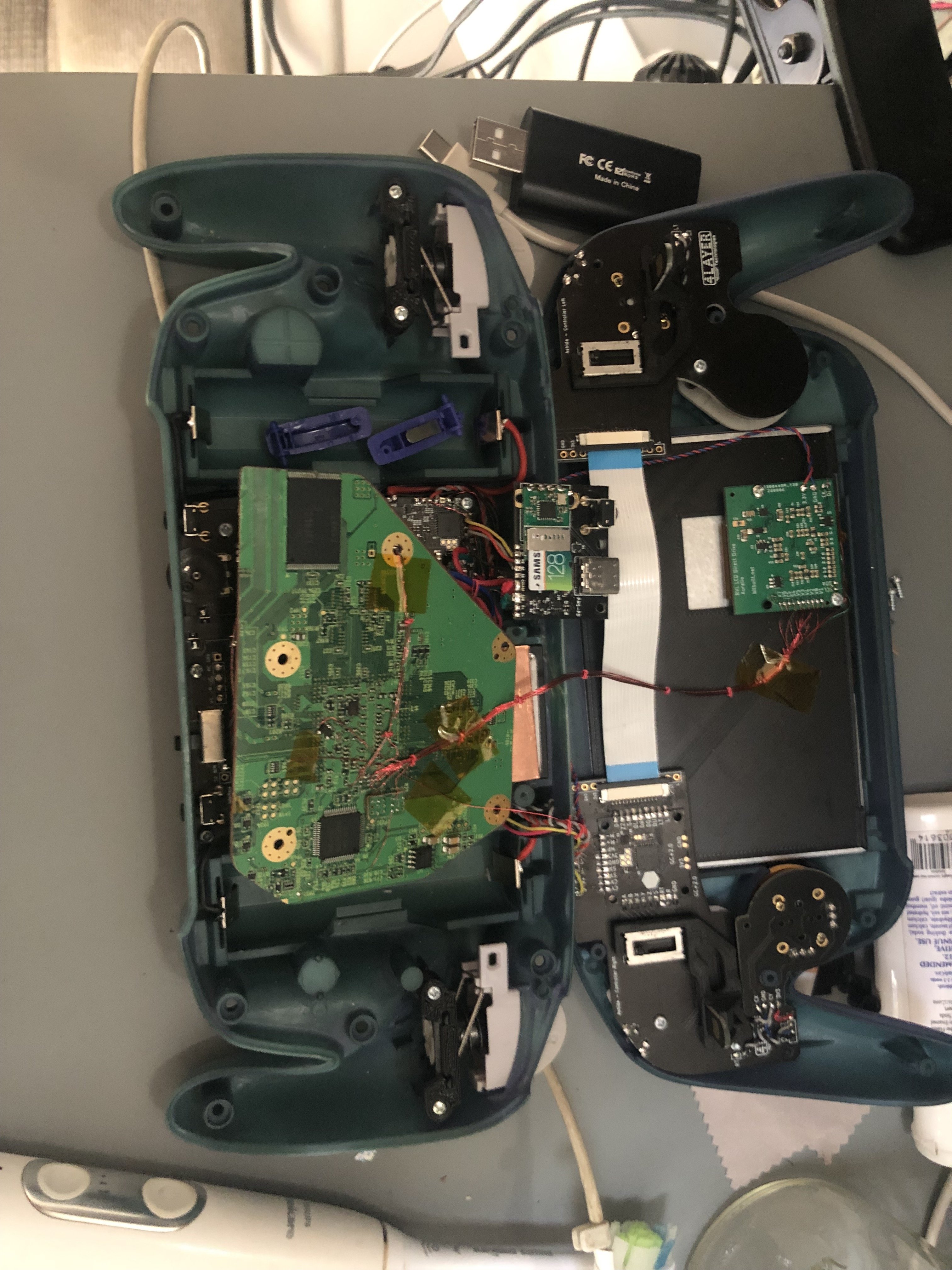
Swapped in a fresh PMSPD and we had all voltages and charging... ship shape. Still a bummer to have two bum boards from the first attempt. It means i get to learn even more about those boards to try to get them back into the line of duty. Progress...
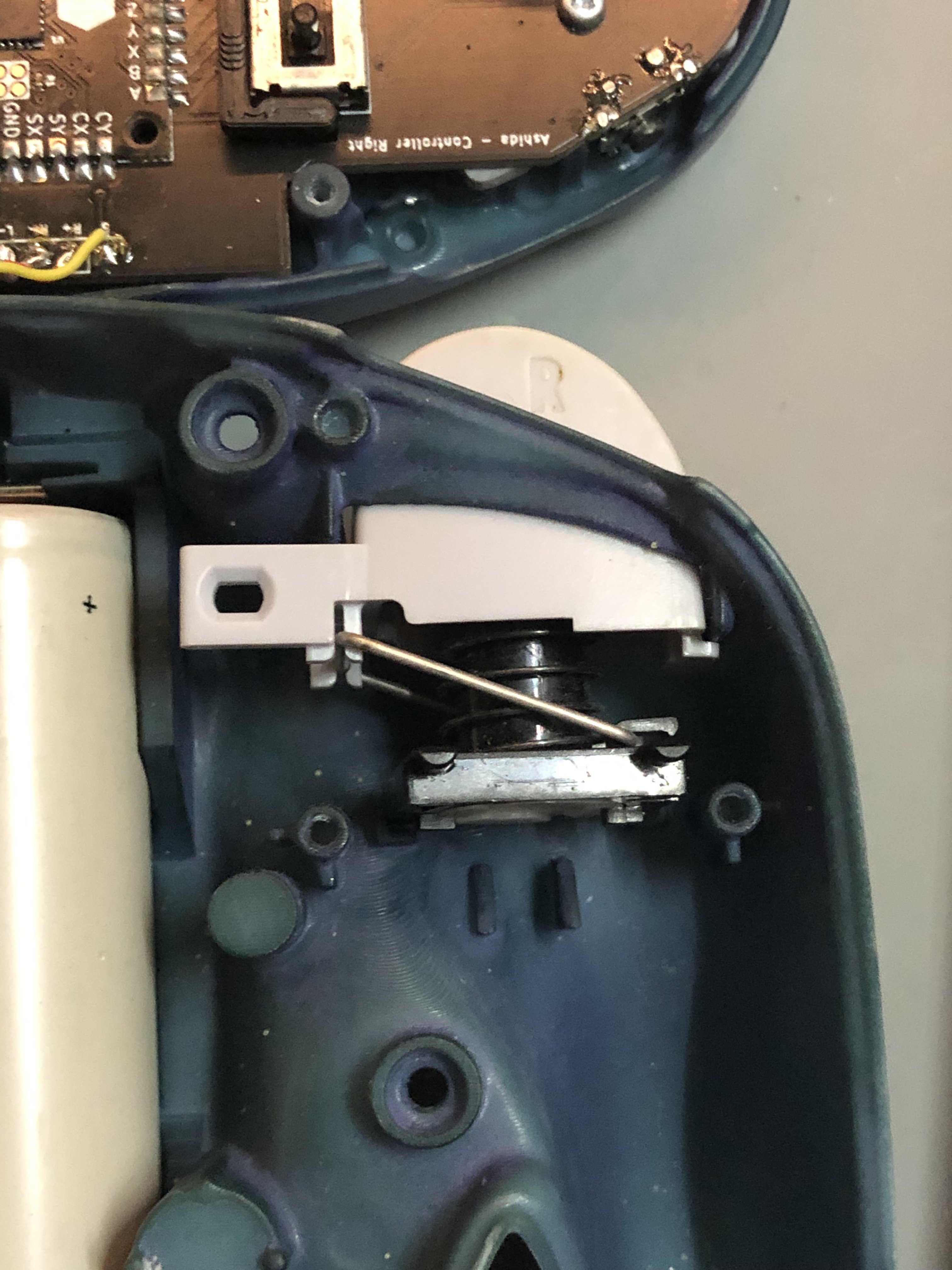
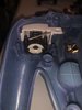
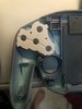
Next was dialing in the shoulder buttons. In button tester, only the analog parts of the triggers worked. Not the full presses. @Wesk Recommended removing the small bracket that holds down the trigger assembly. This allowed the triggers to actuate to their fullest and register the full button press.
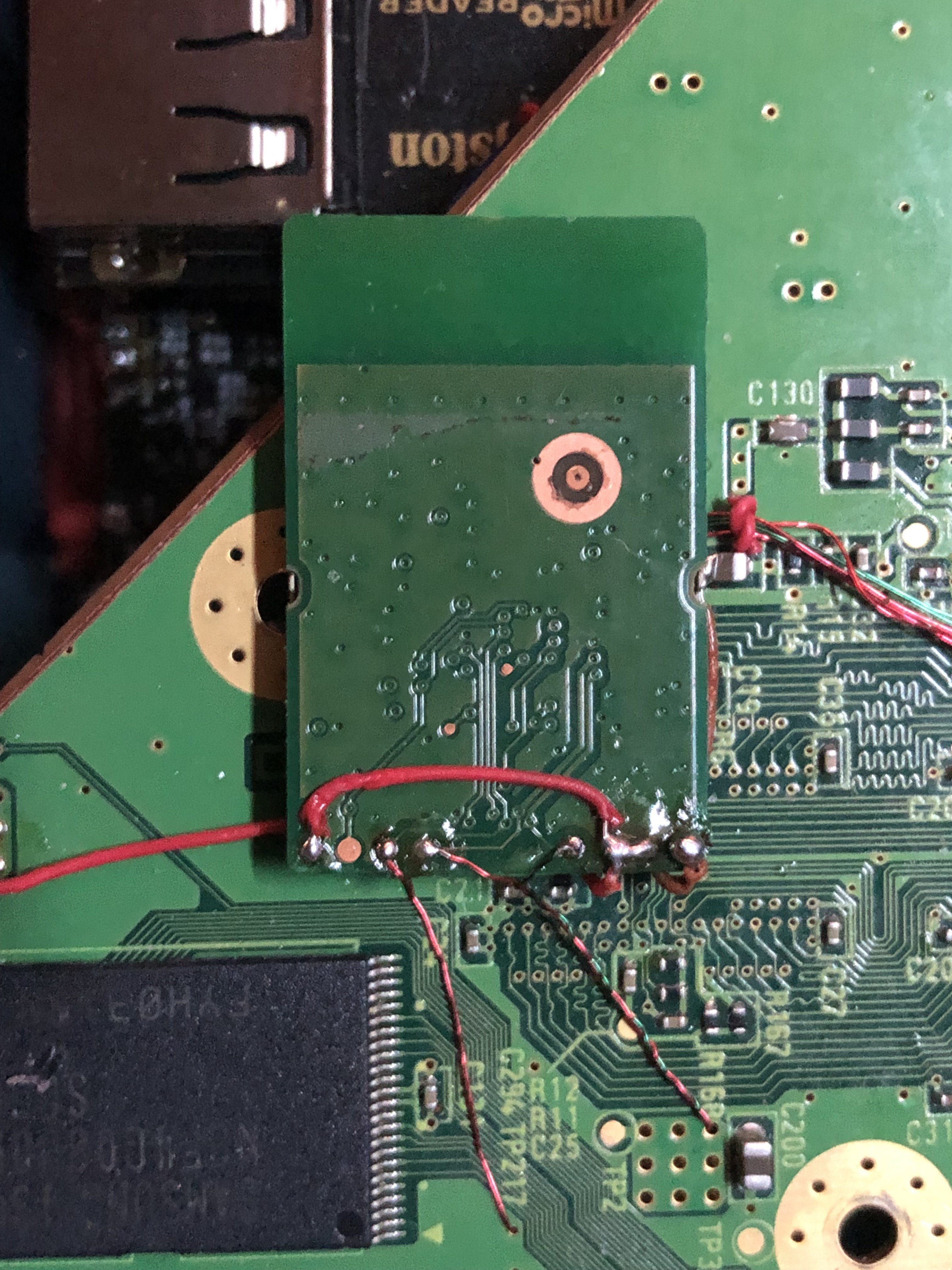
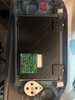
Added bluetooth module. But could not mount on nand as i usually do as the DD takes up that negative space on the other side. Needed to rearrange the layout a bit. Bluetooth relocation was a success.
I tested all functions of the portable (still have yet to do MX relocation) and the only thing out of place at this point is getting the speakers to fire. I know the digital audio lines are OK because I am getting sound in my headphones. I tested and re-tested speaker wiring (R+/- and L+/-) and both lines are connected correctly. Checked orientation of speakers... all as they are expected to be. So, either the speaker switch inside the headphone jack is malfunctioning, or there is an unforseen mis-wiring of analog speaker lines... I do remember @Gman having some sort of issues switching headphone jack on test build. I wonder if the same thing is going on for me.
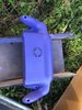
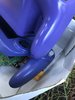
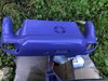
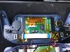
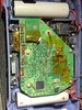
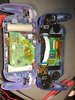
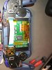
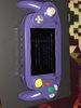
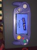
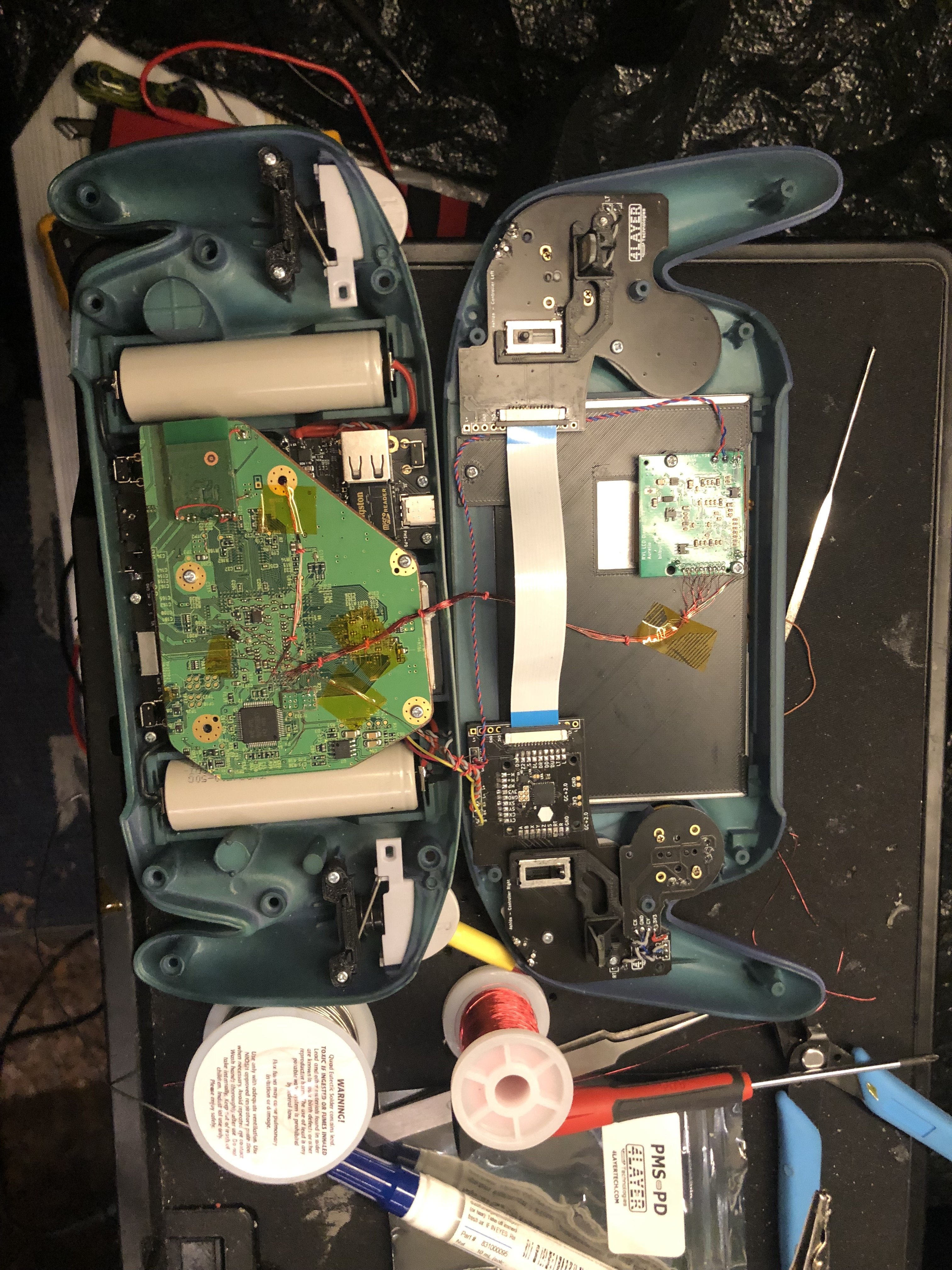
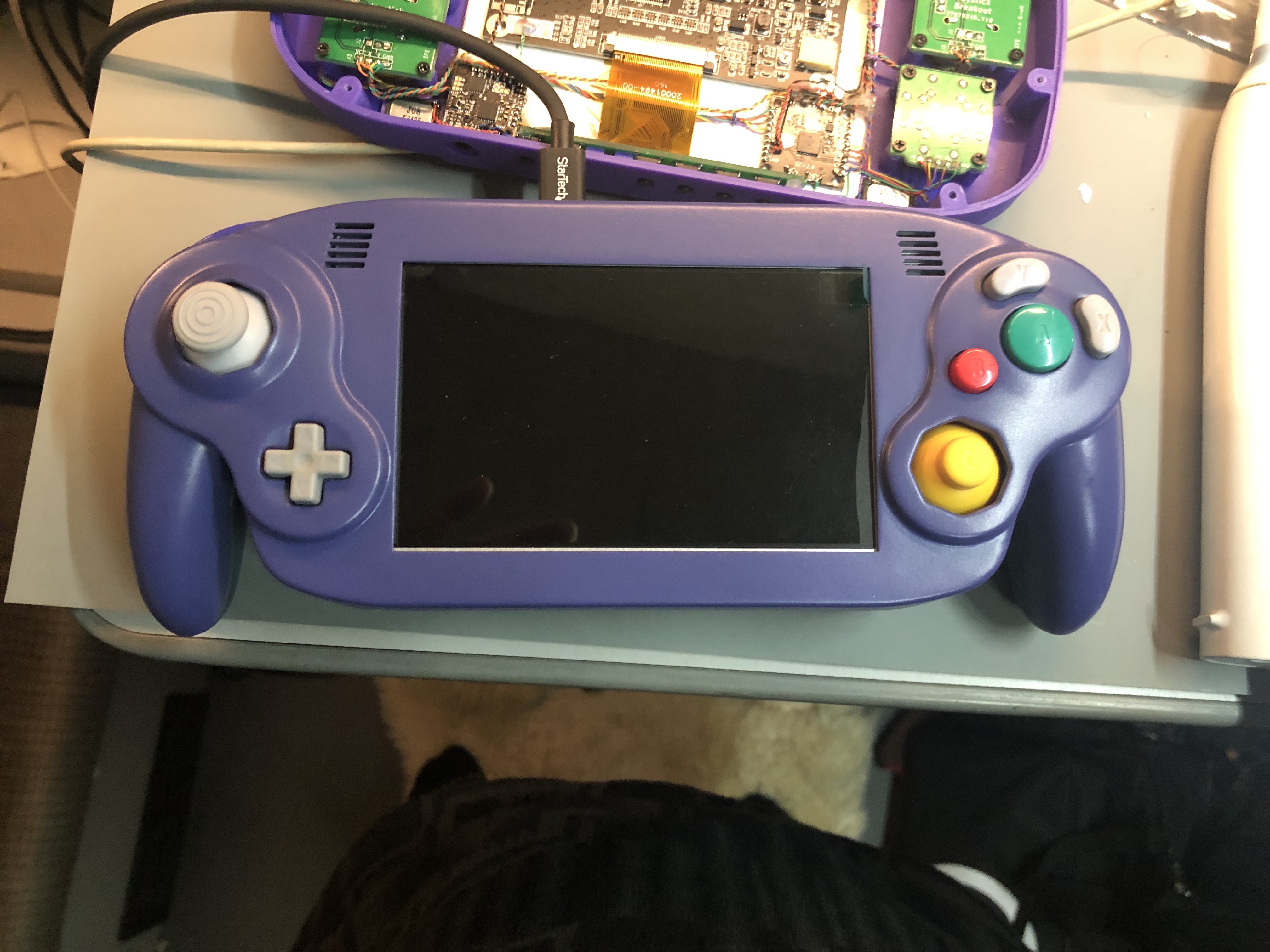
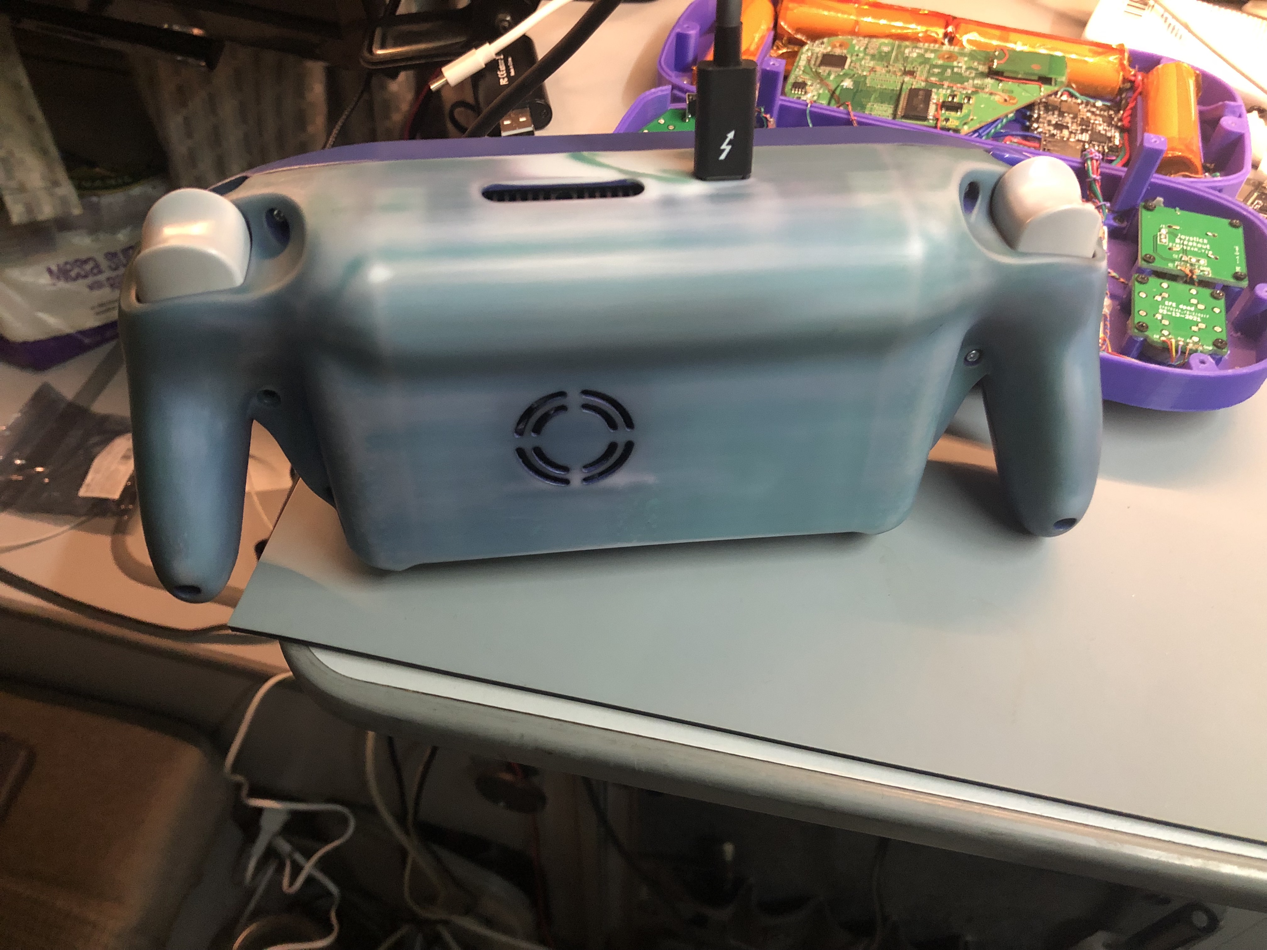
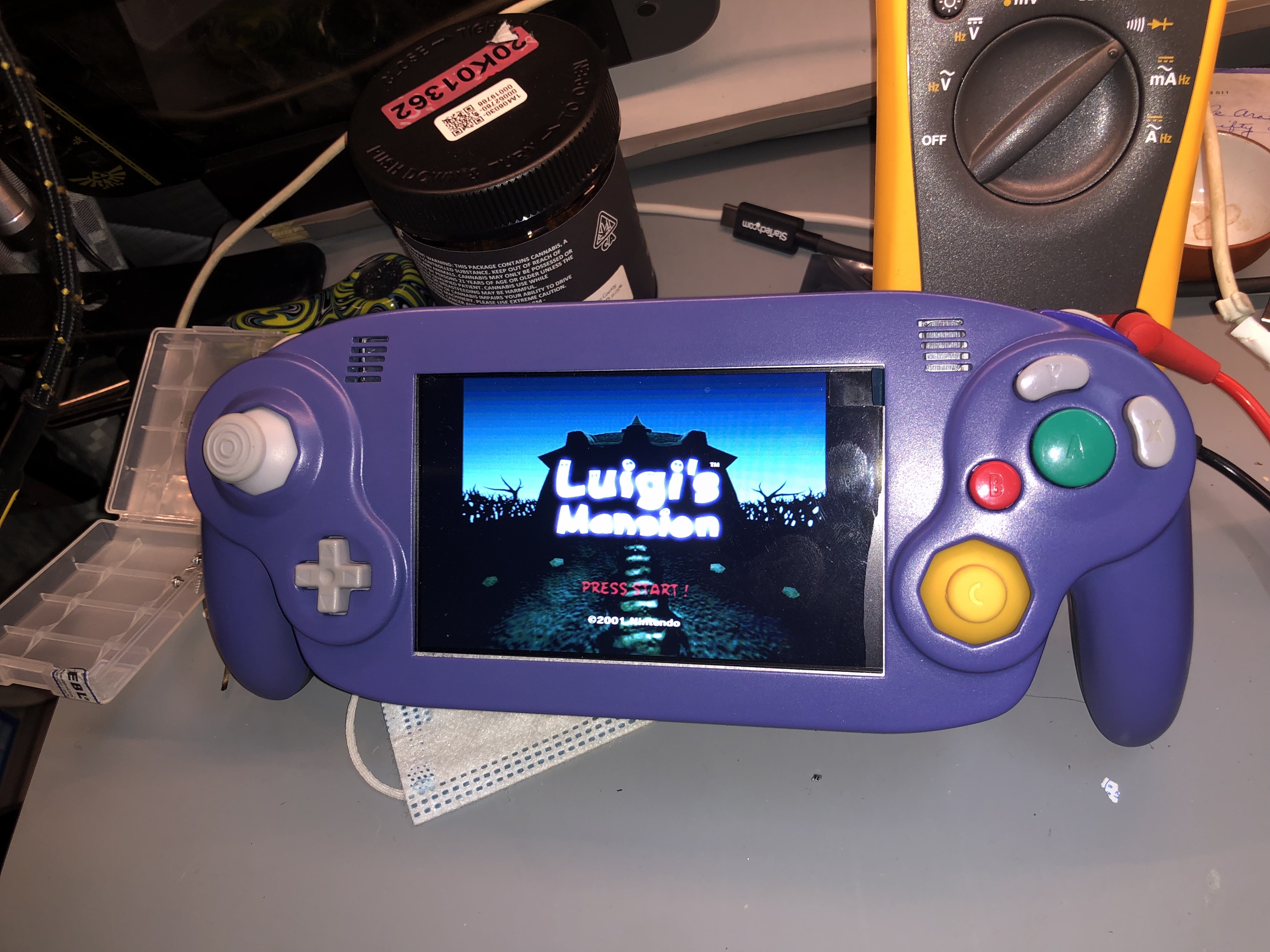
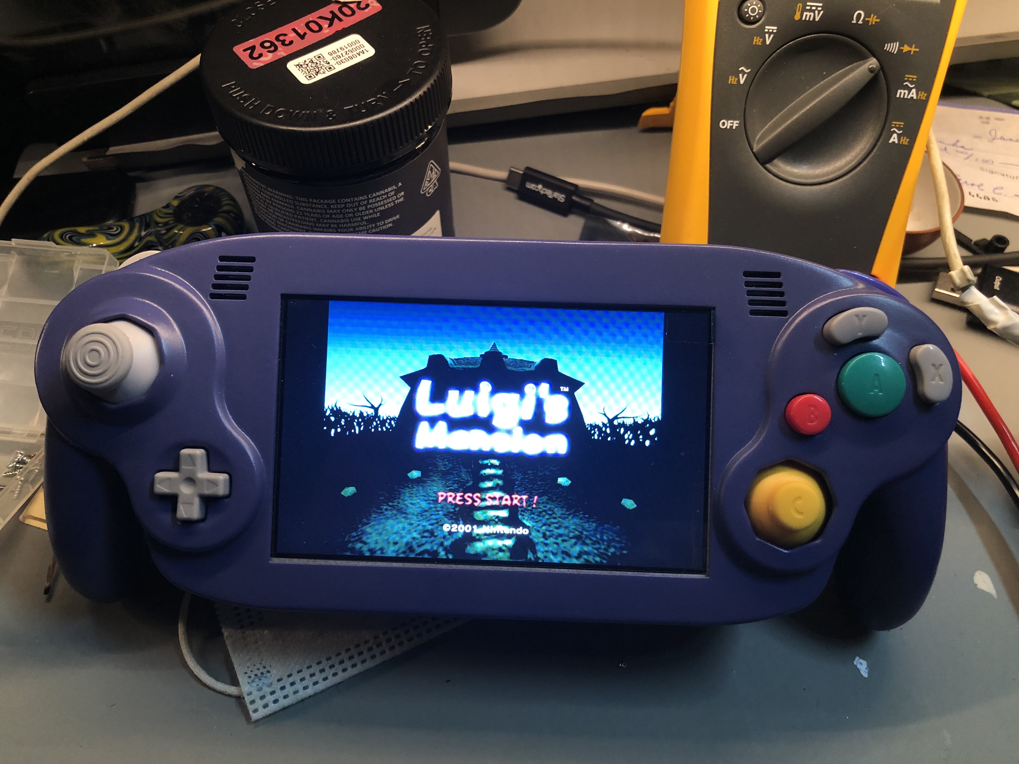
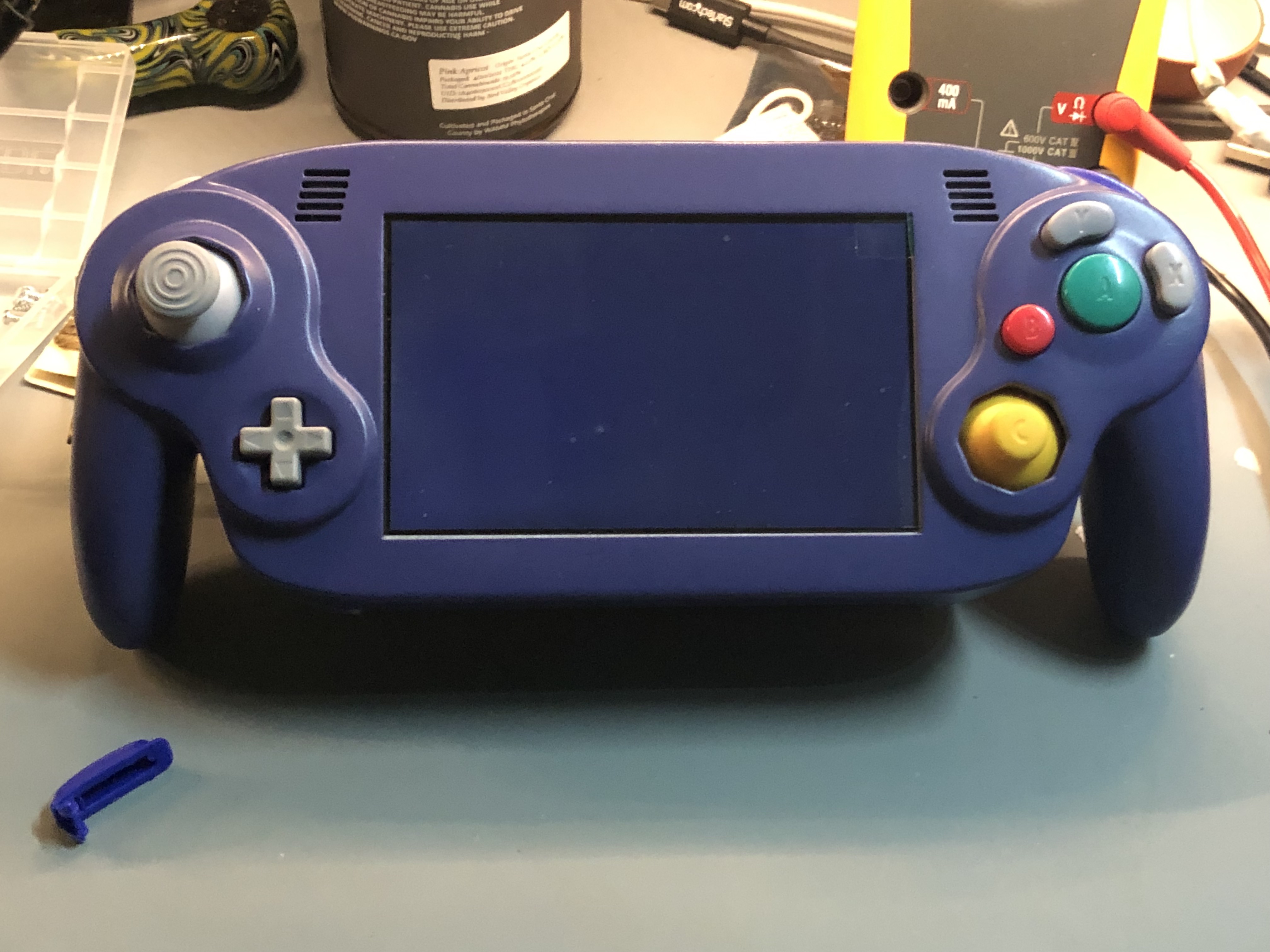
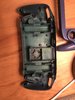
Other than this issue with the speakers this build is pretty much done... Unless, I do actually decide to paint the back... which is likely. But I am glad i got to get through this build with out waiting longer. I do have a utr8100 transparent case waiting for me at my PO box... so i may transfer these internals over to that, repaint and build a second... Or just build a whole other one with the transparent. Anyway. here are some photos of the semi-final internals and outisde.
Still tracking down the analog audio issue... This will get buttoned up soon.
Thanks to @That_Random_Guy for printing me the internal parts.
Special thanks to @Gman and @Wesk for putting this build together. And for also giving me tips along the way when I need help. Its such an elegant and brilliant design. Love it so much! Looks great, feels great, is great...
Cheers everyone.
I ordered the PCBs on day one and soldered all the parts on as soon as they came in the mail. I still didn't have a case though. I took the internal buttons and pads from an official gamecube controller. Got the good stick boxes with the screw mounts. Nice! Mounted all the switches and opted for ribbon cable. I don't think took any pictures of this stage.
A few days after the Ashida was released, I ordered UTR 3100 dyed indigo from PCBWay. The case that arrived was painted as some of you may know the story of my and @Shank 's cases. They were not able to do a good dye job so they just ended up spray painting it.
I was not totally happy with the paint job. Gman had given advice about going lightly and slowly with 1500 grit wet sanding to smooth it out and apply a clear coat. I thought it would be a nice thing so I decided to try to do follow that tip. I had never done any of that before so I kind of took off some of the corner paint. The layer was incredibly thin... woops.
Then, I accidentally smudged the paint with IPA after cleaning a pcb. double woops... This prompted me to just strip all the paint off in hopes of repainting it nicely one day. I used 99% ipa and a clean lint free rag to rub off the paint layers. It has a strange appeal to it... Like a vintaged fender guitar. Except the partially dyed color is only OK looking. In retrospect, the paint job was actually not awful... Learning experiences.
I ordered some paint for the back, but actually couldn't wait any longer to build... so I just went with it. Whatever, it is what it is...
I started on the cooling system... Stuck the fan in with the sticker facing out so the axial fan sucks air in rather than pushing air out through the adjacent fan hole. There is a slot where the wires will pass through unhindered so they can be wired to the PMS. Inserted the two heat sink so that their channel was aligned with the exaust port on the top of the rear case half. Placed in heatsink with fins facing the fan. Prepped a piece of copper that was just big enough to be effective from a scrap I had in my parts bin. Peeled off the adhesive on the heatsink and stuck down the copper.
(i also accidentally left the fan in the rear case in the first few minutes of wet sanding hence the paint stains and loud bearing... ill replace that woopsie one day soon)
Wired up my PMS2 and PMSPD, dropped in the populated Ashida custom PCBs, wired up grounds, battery clips out in shoulder button assembly.
Put leads on voltage lines with color code. One thing I found helpful with the battery clips was not to solder the wires anywhere but the top edge so that the clip could fully seat in the slot. I also ended up running battery wiring through the handy pass through that is a the same depth as the fan in that negative space in the back face of the rear case half. Great layout.
Disassembled the eyoyo ips screen case to discover a BEHEMOTH of a screen driver board that would never fit in the portable. Also, fit caps and buttons into the controller and boards... Its cool I didn't need to modify any buttons or pads for my build... @Wesk said you might need to with some pads but we are not sure. (You will have to modify the Z button plastic male hinge part... just trim/sand the longer nub a bit shorter so both sides are about the same nub size.)
I hadn't planned on using my DirectDrive (DD) board for this project, but it was my only choice if i wanted to move forward with the parts i had on hand. Its a worthy project and a worthy screen. Set the screen in the slot like a glove... At first, I accidentally tried to attach the DD screen mount board with the ribbon set to go OVER the mount... but it actually goes flat against the screen with the mount on top of it... then bends around through the hole to mate with the board. Made a mistake about that at first... Never again. What a cute little board! Was so excited to see what it could do.
Oh, one note about the tact switches for the Z buttons... I didn't have the correct kind that matched the holes in the ashida board. Not sure if anyone was able to source these but I couldn't find them. I ended up just using regular short clicky tact switches, Cutting one side of the legs off and soldered them in place. Using solder, I carefully bridged the mechanical support pads to the front metal face of the tact... this will help support with the stress of pushing the buttons. Be frugal with the solder because it can flow into the plastic part and fuse it in place... this worked perfectly.
Time to do a quick trim and sand of a prepped 4 layer board... easy peasy. I've developed a trim method where after I cut the outline I will use the top face of the cutting wheel to sand the edges at a diagonal to get a good bit of the work done. Its kind of risky but i've had pretty flawless success with it so far. This time I actually got away with only doing a light filing with 200 grit diamond file and then finish with 320 sand paper. No shorts, all resistances were golden. I did the wireless U10 relocation and prepped all the i2c, DD and digital audio via's at the AVE-RVL patch points.
Wired up the Wii to the voltage lines... being sure to route them cleanly and cut them to length. Wired Power and Ground across the case halves to the GC+ board and jumped off of that for the DD power and ground lines. Soldered in the T- wire to the thermistor. Wired up the data lines... (of the two USB via sets, The INSIDE lines are D- and the OUTSIDE lines are D+... put that in the ol memory banks)... Ran the analog speaker wire pairs and start button tact line too. Wired up a temporary RCA cable to the composite AVE via and ground to test booting. Double checked there were no shorts... Popped the batteries in and pulled the switch...And it fired right up! Booting like normal...
Carefully wired 34awg magnet wire to the via points for the DD and ran the labeled bare ends in the direction of the DD. I wanted to run all the lines and tie them off before wiring the other end so it would be a clean bundle. After tying them up I cleanly I cut each to length and soldered to appropriate pad. P1 data wired across top ready to go across the case to the GC+... I knew that i was going to have a few i2c devices that needed realestate at the vias. I tried one of these via fields that i trimmed off of the wii scraps. I thought I'd use one for SDW/SDA and one for SCW/SCL for PMS and DD i2c. However, this actually was the failure point. Maybe the extra layers caused interference?? I couldn't get them to work in the end but at this stage I was gonna try it. I also routed the digital audio wiring across and down to the wire run on the voltage side of the mobo.
Also take note of the trigger brackets, this stumped me at first when wesk recommended I just watch the release video! It shows every part fitting together!
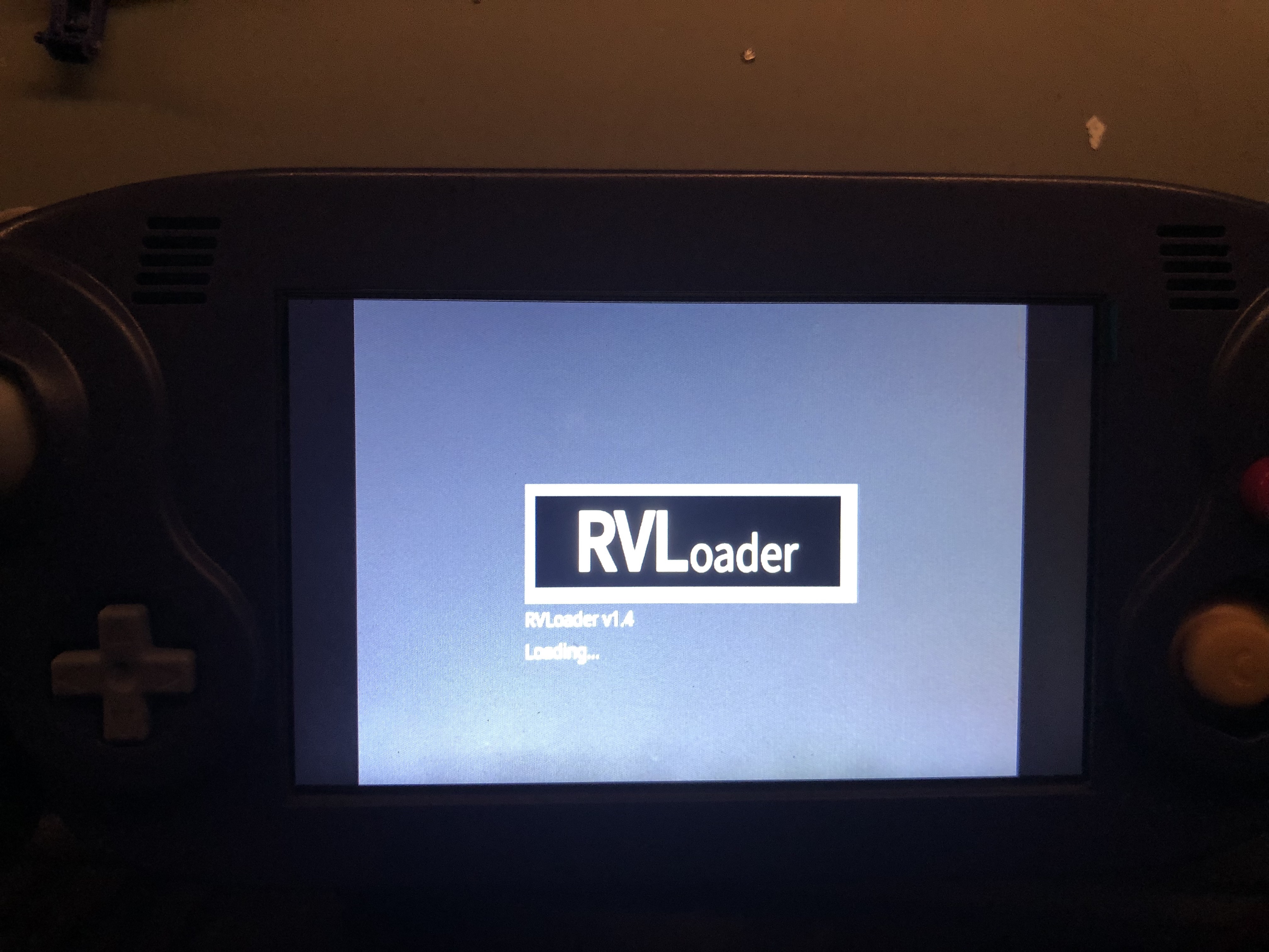
The first test of the DD and Eyoyo screen yielded a crisp and beautiful video signal... Feels good.
However, this is when I started to realize the problems. The PMSPD would not mount the SD card so i thought it needed a charge. The lithium battery I had came with very little charge. So, when I tried to test charging it led to the PMS board fritzing out and I think one of the chips got damaged... I have to inform y'all that the PMS board i used for this build at first was one of the boards i "fixed" from a short circuit mishap weeks earlier. I replaced the BQ chip and it booted up and voltages were outputting properly... I didn't test charging. So, something was wrong... And I believe this led to the PMSPD to also be damaged. I can not know for sure because my intimate knowledge of the deeper workings of these boards are still a bit beyond my understanding... but thats my hunch.
Anyway, PMS2 definitely was not working and by the end of troubleshooting the BQ was getting really hot to the touch with only inserting batteries... I luckily had a PMS Lite on the way from @4layertech that showed up the next morning. I wired up that bad boy next day and we had voltage lines back but still wouldn't mount or charge... 0v at UP and 0v at charging pads. Tried untwisting the SD, SC, PW and UP lines as @Gman advised. Oh yeah, don't forget to run a magnet wire from 1v8 line on the wii at LDO for 1v8 digital logic on the PMS Lite (and subsequently to the uamp)...
Swapped in a fresh PMSPD and we had all voltages and charging... ship shape. Still a bummer to have two bum boards from the first attempt.
It means i get to learn even more about those boards to try to get them back into the line of duty. Progress...Next was dialing in the shoulder buttons. In button tester, only the analog parts of the triggers worked. Not the full presses. @Wesk Recommended removing the small bracket that holds down the trigger assembly. This allowed the triggers to actuate to their fullest and register the full button press.
Added bluetooth module. But could not mount on nand as i usually do as the DD takes up that negative space on the other side. Needed to rearrange the layout a bit. Bluetooth relocation was a success.
I tested all functions of the portable (still have yet to do MX relocation) and the only thing out of place at this point is getting the speakers to fire. I know the digital audio lines are OK because I am getting sound in my headphones. I tested and re-tested speaker wiring (R+/- and L+/-) and both lines are connected correctly. Checked orientation of speakers... all as they are expected to be. So, either the speaker switch inside the headphone jack is malfunctioning, or there is an unforseen mis-wiring of analog speaker lines... I do remember @Gman having some sort of issues switching headphone jack on test build. I wonder if the same thing is going on for me.
Other than this issue with the speakers this build is pretty much done... Unless, I do actually decide to paint the back... which is likely. But I am glad i got to get through this build with out waiting longer. I do have a utr8100 transparent case waiting for me at my PO box... so i may transfer these internals over to that, repaint and build a second... Or just build a whole other one with the transparent. Anyway. here are some photos of the semi-final internals and outisde.
Still tracking down the analog audio issue... This will get buttoned up soon.
Thanks to @That_Random_Guy for printing me the internal parts.
Special thanks to @Gman and @Wesk for putting this build together. And for also giving me tips along the way when I need help. Its such an elegant and brilliant design. Love it so much! Looks great, feels great, is great...
Cheers everyone.
Attachments
-
 976.6 KB Views: 179
 -
 2.1 MB Views: 188
 -
 1.4 MB Views: 182
 -
 1.6 MB Views: 178
 -
 908.3 KB Views: 166
 -
 1,013.1 KB Views: 170
 -
 1.1 MB Views: 166
 -
 828.8 KB Views: 172
 -
 928.8 KB Views: 179
 -
 1.2 MB Views: 198
 -
 909.6 KB Views: 184
 -
 1.7 MB Views: 194
 -
 2.6 MB Views: 198
 -
 1.7 MB Views: 187
 -
 2.1 MB Views: 177
 -
 1.9 MB Views: 181
 -
 2 MB Views: 185
 -
 2.2 MB Views: 200
 -
 1.8 MB Views: 187
 -
 1.7 MB Views: 185
 -
 2.4 MB Views: 177
 -
 1.4 MB Views: 174
 -
 1.1 MB Views: 176
 -
 1.6 MB Views: 195
 -
 3.4 MB Views: 197
 -
 2.4 MB Views: 197
Last edited: