Completed Egg Boy Color

Joined
Apr 6, 2025
Messages
8
Likes
72
Hey all! I'm back for a second year, and intend to finish this time -- as a matter of fact, I've already made it farther than last year by posting a thread.

Setting the Stage
You may know me from my prior projects where I made custom form factor Game Boy Colors using original hardware:
  1. Frog Boy Color: full size, mostly fully featured, wide Game Boy Color -- serious business
  2. Tad Boy Color: small, while still using OG cartridges, most features preserved
  3. Time Frog Color: stupid side quest -- Game Boy Color in a watch, including tiny custom cartridges -- completely impractical
The Idea
As my GBC mods continue to get smaller, and I approach the minimum possible size with the TFC, I think it's time to round out my ever shrinking amphibian themed family with the smallest practically usable GBC I can imagine. And so, I'm Introducing the Egg Boy Color: the answer to the question, "what if Benjamin Button, but Game Boy?"

Key Features
  • Built using original Game Boy Color CPU and RAM for compatibility with original software
  • Compatibility with the same tiny cartridges I designed for the TFC
  • Audio output via speaker
  • Custom tiny buttons
  • Small enough to reasonably fit on a keychain
Stretch Goals
  • Magnetic charging dock using pogo connections
  • Link port support over aforementioned pogo connections
Worklog
For ease of reading, I will post a summary of worklog entries in this main post in addition to more fleshed out ones as separate posts.

5/23/2026
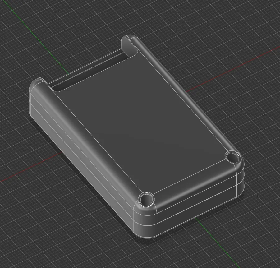
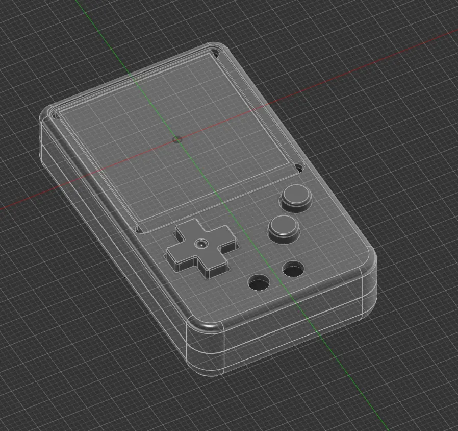
Project kickoff! Started working on the main shell design, both front and back. Front shell is designed around a 1.54" 320x320 IPS screen so I can get a clean 2x upscale on the GBC video.

Fusion360_lzAqSHxj6e.webp
Fusion360_m1LD2tgZB8.webp
 
I love your work! I plan on getting a Tad Boy Color very soon. I’d like to make one but I’m gona have to get it commissioned. Could you recommend anyone?
 
Got started on the Egg Boy Color electronics this past weekend by designing an RP2040 development board for the main LCD candidate that I'm considering for this project.

LCD Info

Model: ET015SQ05
Size: 1.54"
Resolution: 320x320x16bpp
Interface: SPI, ST7796U driver

I've also attached the datasheet for this LCD so you don't have to email them like I did.

The units I have appear to have been manufactured in late 2019, which I'm hoping isn't a bad sign for future availability. At the very least, I've found multiple Chinese sellers using what looks like the same panel with slightly different flex bridges. I'll be sampling some of those to determine compatibility. Fingers crossed, since this resolution at this size doesn't seem to be widely available, outside of some MIPI panels.

LCD Dev Board

kicad_xgSINwyKir.webp
kicad_wdW3PZrpPF.webp


The LCD dev board is an RP2040 carrier board -- based off of the minimal circuit implementation from the RP2040 datasheet -- that is purpose built to test both the screen driver circuitry, as well as the firmware for translating the GBC video signal to SPI for the new LCD.

On the back of the board is a 50-pin FFC socket that connects to a standard Game Boy Color. The video signals from the GBC -- pixel data, pixel clock, H-sync, and V-sync -- are routed to GPIO on the RP2040 through this connector. 3.3V is also carried over the connector to allow the dev board to be powered by the GBC.

The other connector on the back is the 24-pin mezzanine connector that the LCD will plug into. This was actually one of the trickiest parts of the design, as the LCD appears to use an obsolete connector, the OK-22M024-04. It's a 0.4mm pitch 24-pin male connector with a stack height of 0.7-0.9mm. I was unable to find stock of the equivalent female part anywhere, so I had to take measurements and dig through datasheets for similar parts.

After some trial and error, I'm now fairly certain it's a clone of a KYOCERA AVX part. Test fits show it mates well with the 245804024000829+ female connector, so unless I discover later that the pins actually don't connect quite right -- not going to know that until I have the dev board and start powering things up -- that mystery appears to be solved.

The only other interesting parts on the board are LDOs for 2.8V and 1.8V rails. These are required by the LCD, at least according to the datasheet which is somewhat vague on exactly what this thing wants. The SPI lines appear to be 3.3V tolerant according to the datasheet, so I assume there's some level shifting happening internal.

What's Next?

I've ordered the dev boards, so I expect those to arrive in the next couple weeks, and then I can assemble and start testing things out.

In the meantime, I think next I'll start refining the EBC shell, specifically focusing on the buttons since they're still in a bit of a rough shape.
 

Attachments

Last edited:
After seeing your other projects, im suitably hyped for this one! Good luck and God speed!
 
Despite my lack of worklog entries over the last 3 months, things have been rolling right along. However, because of the large amount of information there is to go over, I'll be splitting up the updates by workstream over the next few days. Today, I'll be going over the electronics.

EBC-LCD-DEV1

Picking up where I left off in the previous update, I'll briefly discuss the EBC-LCD-DEV1 board. In short: it worked. There was very little drama with the actual hardware, beyond an error in the LCD datasheet -- pin 15 was marked as D/C for the SPI interface, but it's actually pin 16. A quick bodge had things up and running pretty quick.

chrome_9yJxV5pFCQ.webp


The software side of the LCD driver ended up being an absolute shit show. TL;DR: this LCD does not support the SPI clocks necessary to hit the bandwidth requirements for a 2x scaled GBC image, and in some cases you can't always trust the SPI clock you think you're at. However, I'll save most of that story for the next update.

EBC-CPU-X1: Schematic

With the hardware side of the LCD driver proven out, I moved on to the schematic and layout for the integrated EBC motherboard, designated EBC-CPU-X1 -- in keeping with Nintendo naming conventions.

The actual schematic design was a pretty simple affair. This is, after all, my 4th custom GBC motherboard design, so I have a solid understanding of that side of things. And because I had already designed a separate dev board for the LCD driver that interfaced with a GBC, it was just a matter of smushing the two schematics together, and directly routing all of the display signal lines from the GBC CPU to the RP2040 instead of through connectors.

The net-new pieces of the design are power, charging, and audio.

For power, I needed to generate 5 different voltages:

5V -> GBC IO
3.3V -> GBC core and RP2040 IO
1.1V -> RP2040 core voltage
1.8V and 2.8V -> Required by the LCD for reasons I'm not privy to.

kicad_bTm6uLXCn0.webp


You might notice that I've chosen to implement an external 1.1V source for the RP2040 using a boost converter, in contrast to most RP2040 designs I've seen, which simply rely on the MCU's integrated 1.1V LDO. For a larger device, or one that's intended to remain plugged in, I wouldn't have bothered. But because the EBC can only fit a small battery with a capacity of ~200mAh -- and because the RP2040 cores will be constantly working -- I wanted to ensure that it was as efficient as possible.

Charging is handled via my beloved BQ24072, which is a linear charge IC from TI. The nice part is that it integrates power path management, so system power is automatically switched between battery and USB VBUS when a charging cable is plugged in.

kicad_MskNjYcj0R.webp


Audio is a very simple affair. All Game Boys support stereo audio, but because there's only room for one speaker, and none for a headphone jack, the two channels are simply ran through their own DC block cap and resistor before getting merged at the audio input of the amp. No room for my beloved and totally non-controversial volume wheel, so volume control is handled via PWM from the MCU.

kicad_uA30rTmUe6.webp


Not shown, but I also added PWM brightness control for the backlight -- also from the MCU -- as well as a voltage divider that halves VCC(battery voltage) and connects it to a GPIO on the RP2040 for a software battery indicator(TBD).

EBC-CPU-X1: Layout and Routing

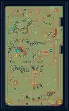
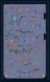
I'm the wrong person to discuss PCB layout in any detailed or meaningful sense, but this was where most of the effort went with this board. It's a 4-layer 0.8mm board, and holy shit, layout and routing was a nightmare.

kicad_i08yNhTVlF.webpkicad_CJWqtH2zSz.webpkicad_zpqUIsbJL9.webpkicad_InDhPdROXd.webpkicad_S5M7VQbSDT.webpkicad_tFGd6AP6Cz.webp

In hindsight, I would have had a much easier time if I had gone with a 6-layer board and just sucked up the added cost. While I tried to keep by internal power and ground layers as clean as I could, some of the signals ultimately ended up getting routed on them because of just how close together everything is. I'm also inept and a bit of a dummy, so that certainly contributes.

EBC-CPU-X1: Testing

In comparison to layout and routing, assembly and testing was actually a breeze(with one caveat, which I'll get to). I used a past stencil and a hot plate for most of the assembly, which made even the tiny QFNs easy peasy lemon squeezy. I was quite chuffed to see it booting to a familiar screen.

eggboybooted.webp


The frustrating part of all of this was that the pictured unit is in fact the second one that I assembled, because I couldn't for the life of me get the first one to actually boot into a game. Even worse, I initially couldn't get the second one to do so either, which really had me worried that I had messed up the schematic somewhere -- it seemed exceedingly unlikely that two separate boards would have an assembly error resulting in the exact same problem.

However, you might notice that there are no tac switches installed in the picture, and this is related to the cause of my woes. While verifying some ground connections on the CPU, my multimeter probe slipped onto one of the pins for the buttons, and I got a beep. Checking each of the buttons, I noticed that they were in fact all shorted to ground.

Turns out I had installed every single button rotated 90 degrees out of the correct orientation, which resulted in all of them registering as pressed all of the time, and it turns out that certain games -- including the two games that I tested, Tetris and Mario Land II -- absolutely hate that. Everything booted right up as soon as the buttons were removed, and things just worked after putting them back in the correct orientation.

So we're in business! The core thing works.

EBC-CPU-X1: Misc. Learnings and Future Plans

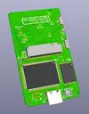
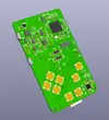
The eagle eyed among you might notice that the board renders actually say EBC-CPU-X2, and that's because I'm writing this in hindsight, after having pulled together a second revision, though not yet ordered. Changes are discussed below.

MCU controlled GBC reset

The reset line of the GBC CPU will now be controlled by the RP2040. This is largely to give me control over the entire system boot sequence so I can put a nice level of polish on things -- currently, the Game Boy boot screen initially appears mid-way because it takes some time for the RP2040 to boot and initialize the LCD.

Fixed GBC boot bug

I fixed an interesting issue -- also related to GBC reset -- that would cause the GBC portion to not boot the first time you try to power it on, but only when the battery level was above a certain point. This turned out to be a power sequencing issue.

In short, the 5V regulator has a soft start feature that makes startup time dependent on the regulator input voltage -- the higher the voltage, the faster 5V comes up. Because the reset IC is monitoring the level of 5V, and pulling CPU reset LOW below ~3.1V, higher battery voltages cause reset to go HIGH relatively early. This happens faster than the 3.3V rail can come up, and the CPU ends up in a bad state, being out of reset but with too low of a core voltage.


The MCU controlled reset is incidentally one fix for this, since it will allow me to implement a delay in software before pulling the CPU out of reset, beyond what the 3.3V rail should take to start. The second was simply tying the CE pin on the 5V regulator to the output of the 3.3V regulator so that 3.3V always comes up before 5V.

What's next?

In the next update, I'll go over the final design and fabbing of the shell.
 
With the electronics out of the way, I'll now talk a bit about the shell: what changed since the original log entry, how I fabbed it, and how it has turned out.

The Final Design

The final design remains largely consistent with the original work that was done -- it got a couple millimeters thinner, but otherwise most of the changes made were either internal, or made to accommodate features that needed to be exposed externally in any case: speaker holes, buttons, screw holes, etc. The only notable callout, is that I settled on USB-C for charging instead of the pogo connections, so there's now a cutout for that.

Fusion360_SUmJ65ro4N.webp
Fusion360_uNS3m6JsGH.webp


The inside, however, has undergone significant changes, which is to say: it went from basically nothing, to the rest of the fucking owl, to use the parlance of our times. Standoffs for the motherboard, speaker well, walls around button holes to keep the buttons in place and hole membranes. There are also a lot of cutouts on the back shell to prevent collisions with parts on the motherboard -- these frequently evolved as the board changed, or -- more commonly -- as I forgot there was a part somewhere when fabbing the prototypes.

Fusion360_XiEmuM7e54.webp
Fusion360_o0TRyZcnDi.webp


Milling

I do very little to maintain my 3D printer, and as a result, it doesn't print so well anymore -- because of this, I pretty much just went straight to milling the shell out of aluminum on the Carvera Air. That said, unlike previous projects, I spent a lot of time getting the design right the first time, instead of churning out dozens of prototype prints.

The first and only prototype for the front shell was mainly to test lens and LCD fit. I actually streamed a good chunk of the CAM, setup, and milling for this first prototype, which you can checkout on my YouTube channel if that interests you.

chrome_whTKj7Behc.webp
chrome_Ck2wKxiWRV.webp


I did no more prototypes for the front shell after verifying the important parts fit, and went straight to fabbing what will become the final shell for the initial unit.

chrome_WzNqQrK9xQ.webp
chrome_NPO5KaaFcr.webp


I did 3D print a test back shell so that I could get a feel for an actually functional unit -- this was after I had assembled and tested the first motherboard -- and I'm glad I did, because some of stupid motherboard parts I mentioned before showed their stupid faces and got in the way. Better to catch those on a quick print, instead of a an aluminum part that I then have to rework. I quickly followed that up with an aluminum version once the fit issues were fixed.

chrome_myq9kgm0CE.webp
chrome_ku5jSdfW7D.webp


Surface Finishing

The final thing left to do after milling the shell was to surface finish it, which constitutes two parts:

1. Bead blasting to hide machine marks and give it a nice feel
2. Anodizing to allow dying and provide scratch resistance

Bead blasting is a relatively simple process, although I did ruin the first front shell I made because it turns out high velocity glass beads can and will deform thin sections of aluminum. RIP in the peace to the speaker area on that one.

chrome_EPaRo1W5iE.webp
chrome_OqlppbVa0H.webp


Anodizing is a much more involved process, utilizing various chemical baths, and introducing a bunch of pit falls that need to be looked out for. The process I followed:

1. Thorough cleaning of the parts

2. Electropolishing in 85% phosphoric acid, which yields a much shinier final finish post-anodizing. This generally requires a heated solution, but I found that the amount of power getting dumped into the bath during the process -- up to 150W in my case -- was more than enough to thoroughly heat my small container.

chrome_rpVKcOJRio.webp


3. Again thoroughly cleaning the parts.

4. Anodizing of the parts in an acid solution -- I use a constant current strategy, where I target ~6 amps of current for each square foot of part surface area, capping the voltage at 20V. I don't like the idea of keeping concentrated sulfuric acid solution around my house, so I use a solution of water and 20% by weight of sodium bisulfate, which is generally used for lowering the pH of swimming pools. It's not quite as effective as sulfuric acid, but is in general safer, and comes as a bag of dry crystals, which is much easier to store.

5. Thorough rinsing of the parts.

6. Immediately placing the parts into a heated dye bath for ~15 minutes. I initially thought my anodizing had failed, as the dye didn't appear to be soaking into the oxide layer, but it turned out that I prematurely placed the parts before the bath had heated enough -- 85C is the general target for the Caswell dyes I'm using.

7. Another thorough rinsing of the parts.

8. Immediately placing the dyed parts into a near boiling solution of nickel acetate to seal the pores in the oxide, thereby locking the dye in place, hopefully permanently. Boiling water also works -- though not quite as well -- but I already had a solution of nickel acetate that I've been using for nickel plating items.

9. Tada:

chrome_T4LposU2VE.webp


What's Next?

With the shell complete, I'll move onto the buttons in my next update -- that should be a shorter, but hopefully still interesting update.
 
Moving on to buttons, which -- unlike most other console mods, which use existing commercially produced buttons -- are bespoke, due to the small size of the system.

The Design

In short: they sure are buttons. The initial intent was to make monolithic buttons -- that is to say, buttons with integrated membranes -- out of injection molded silicone, the design for which you can see below.

Fusion360_fjvoMLlXok.webp
Fusion360_ja74RTXGwM.webp


I actually made the mold for these and did some test castings, but unfortunately, the silicones I had on hand at the time aren't fit for this purpose -- some 50 Shore A silicone that's east to cast, but too soft to be playable; and some 60A that's far too viscous for me to properly cast with hand equipment. You can see some tests with the 50A here, which look sick as fuck, but sadly feel gross.

chrome_QtGUIZTq9I.webp


I have recently procured much more easily workable 60A silicone that should work well, so I absolutely intend to get back to this concept, especially since I already have the mold. I think it will open up a lot of cool visual looks that are otherwise tough to get with milled or printed buttons.

That said, for the moment I've moved on to traditional buttons and membranes for the sake of time, which probably sounds ridiculous at first given the need to make traditional membranes and buttons.

Lucky for me, the design change is easy enough by just slicing the monolithic buttons down the middle and adding some registration features on both halves.

Fusion360_d5XW3BZDu1.webp
Fusion360_rVpvEOl1YV.webp


Making the Membranes

The membranes -- and the monolithic buttons that preceded them -- are injection molded using a simple two part mild steel mold that I milled on the Carvera Air. Normally I make my molds for silicone from aluminum, but I wanted to try steel to see if it would reduce sticking and increase longevity -- only time will tell if that thought bears out long term, but they sure are pretty and could be used to kill said aforementioned bear if circumstances necessitate it.

Below you see the mold for the full silicone buttons, but thankfully the change to standard membranes only required milling a new top mold, as the bottom features were completely unchanged.

chrome_nL3rWLfMwR.webp
chrome_mqja7PLY1q.webp
chrome_mo7SWVlaZB.webp


Making the Buttons

The buttons, despite their small size, are actually quite easy to mill. I've milled two sets now -- one from aluminum, and another from delrin(incredible plastic, holy shit) -- using a technique called window machining, where the parts remain suspended within a stock billet via tabs that are then cut and ground away. This allows me to do all of the buttons in two operations, instead of having to individually hold and locate each button in a vise or collet.

chrome_6XejBwqIj2.webp
chrome_BvFj61n80d.webp
chrome_I8LHAzHlQ0.webp


The Troubles

Beyond the issues with the all silicone buttons, things have not all been smooth sailing.

The pips on the bottoms of the membranes that actuate the tac switches were initially too small, causing problems filling completely during molding, and even when successful, having too much give to provide a good feel when pressed. Fixing this involved reworking the mold to make the pips bigger, and doing what I could to get a good cast from the thick-ass 60A silicone, which I eventually did manage to do.

More of an issue was the D-pad, which required a bit more refining, mostly in regards to the diameter and length of the pivot. The aluminum buttons I made have a pivot that is too wide, which can end up bridging pins on the tac switches and creating false inputs -- this was fixed for the next revision. Then I had issues with the length of the pivot -- too short and you can press all of the directions at once, but too long and you can't press anything. The length difference between these two outcomes is roughly 0.2-0.3mm, so we're talking quite tight tolerances to get this working right.

However, in the end I did get it working, and now I've got a set of buttons that feel most excellent.

chrome_BZhETxWXfW.webp


What's Next?

In the next, penultimate update I'll cover the software that has gone into this thing -- because despite being a real GBC at heart, the screen and such require such nonsense.
 
It's finally time to talk about the software for this thing, and all of the woe that has come along with that.

A Quick Refresher

As previously noted, despite the Egg Boy Color being a legitimate GBC with the OG GBC chips, there is software involved, which handles three key things(and one future thing)

1. Converting the image signal from the GBC CPU into a compatible signal for the new display
2. LCD brightness control
3. Volume control
4. In the next revision, control over the GBC CPU's reset signal

This update will cover the first three things, but mostly the first.

Driving the LCD

In principle -- and largely in practice -- pulling the GBC image data and driving the LCD is a relatively simple affair.

The Game Boy Color uses a simple parallel RGB interface, which boils down to a VSYNC, HSYNC, pixel clock, and 15-bits of color data that update prior to each pixel clock pulse. In my case, I use a couple of PIO programs on the RP2040 to monitor the timing signals, pull in color data, and then dump that into the TX FIFO queue.

External to the PIO, there are two chained DMA routines that watch the TX FIFO and move the incoming data into a frame buffer until the buffer size has been hit. The reason for the chained DMAs is because I'm using a double buffered setup -- each DMA is assigned to one of the buffers, and during the DMA completion handler, the active buffer flips and the next DMA is kicked off.

I didn't feel like faffing about with writing my own software for interfacing with the LCD, so I opted to use the TFT_eSPI library, which supports SPI communication with a wide array of LCD driver ICs, and has a bunch of helpful features baked in, like window addressing for writes. As soon as a frame is ready -- and the TE signal from the LCD indicates the start of a new frame -- the contents of the most recently completed buffer are sent to the LCD.

The Scaling Problem

As great as it would be, modern LCDs with a resolution of 160 x 144 are essentially non-existent, which requires the use of something with a higher resolution. As previously noted, I chose a small 320 x 320 panel that allows me to use a clean 2x integer scale to fill the entire screen.

Unfortunately, this is where things start becoming difficult. Integer scaling is by itself a simple thing -- taking an image of a given size and scaling it into an appropriately sized buffer is easy. However, doing so within the RAM and CPU limitations of an MCU becomes more difficult.

RAM is by far the biggest issue of the two, with a single 320x288x16bpp buffer using ~184kB of RAM, which is nearly 3/4 of the RP2040s 264kB -- 2 buffers simply won't fit.

The question then becomes: why not use smaller 160x144 buffers and then scale them up to 320x288 before? There are two very good(allegedly) reasons for not doing this:

1. Doing so requires additional CPU cycles to scale the image -- this eats into CPU budget that's needed for other duties
2. Scaling still requires an additional buffer that is at a minimum 320x144. This along with the two native size buffers total that same 184kB mentioned earlier -- not unreasonable, but not worth it when bundled with the CPU cost.

As such, the approach I've taken is a bit different, and gets me all of the scaling more-or-less for free -- as an added bonus, the implementation is very simple.

In the PIO program that ingests pixel data from the GBC CPU, I simply push each pixel out to the TX FIFO twice, effectively a 2x horizontal scale for free since there's additional time budget in the PIO. For vertical scaling, I can simply draw each line twice across two LCD lines -- or just leave every other line blank. This way I maintain only two buffers sized 320x144 for that same 184kB RAM cost, and get to skip most of the CPU time needed to scale traditionally.

Ill Tidings

With scaling figured out, you'd think the rest would be simple since we can already draw to the LCD. However, the big thing that I haven't gotten into yet is SPI bandwidth.

SPI is a serial communication protocol, which means it transmits a single bit per clock pulse. This means to transmit 60 frames that are 320x288x16bpp requires an SPI clock of a bare minimum of ~88MHz, with some additional to provide overhead for the SPI instructions needed to setup draw calls.

History tricked me into thinking this wouldn't be an issue. The Time Frog Color uses the same strategy, with some additional shenanigans to upscale by 1.5x to fill the 240x240 panel, but still for "free". The bandwidth required for that is ~50Mbp/s, which worked fine despite the ST7789 LCD driver IC being officially rated to only handle something like a 20MHz SPI clock. I was -- seemingly -- able to bump SPI clocks as high as 100MHz with no issues. Incredible.

The ST7796 in the Egg's panel is rated similarly, but initial testing indicated that I couldn't bump the SPI clock quite as high -- 50MHz seemed to be the ceiling. That's fine! I can just do that thing I mentioned earlier where I leave every other line blank, which cuts the necessary SPI clock to 44MHz -- barely in budget, but it works, and nerds love "scanlines", as it were.

Shit Hits the Fan

All of this was figured out back when I was still working with EBC-LCD-DEV -- as it should, as that was the whole point.

Sadly, things are not always as they seem, and it turns out I hadn't done sufficient testing before patting myself on the back and calling it a day. As soon as I assembled the initial motherboard and got it booting games, I noticed that things were not running at full framerate, like originally thought. Games played smooth... ish, but there was a lot of tearing. Tying screen updates to TE ending up hard locking the framerate to 30FPS, which was odd given my prior bandwidth calculations. No matter, I thought, I'll just play with SPI clocks to see if I can go a bit higher than my prior tests.

This is when shit got weird.

While testing out various SPI and RP2040 clock combinations, I noticed that there were a number of cases where higher SPI clocks performed substantially worse than lower clocks -- not unstable, mind you, just worse. This made me question whether or not the SPI clock I was configuring -- which was done through the TFT_eSPI config -- was actually the same as what was being generated.

I was basically tearing my hair out at this point, because it didn't make a lick of sense, and I was on the verge of pulling out the oscilloscope to start poking around. Then I made a breakthrough.

C++:
// Set clock divider, frequency is set up to 2% faster than specified, or next division down
uint16_t clock_div = 0.98 + clock_get_hz(clk_sys) / (clock_freq * 2.0); // 2 cycles per bit
sm_config_set_clkdiv(&c, clock_div);

This is the code in TFT_eSPI that sets the PIO clock divider based on the configured SPI clock. This piece of shit, for reasons that I haven't been able to piece together, is intentionally truncating the result of this float calculation to an int, and the closer the system and SPI clocks are to one another, the the larger the possible error gets.

Some examples:

SPI(configured): 40MHz, SYS: 120MHz -> clock div of 2 -> SPI clock of 30MHz
SPI(configured): 50MHz, SYS: 200MHz -> clock div of 2 -> SPI clock of 50MHz
SPI(configured): 40MHz, SYS: 200MHz -> clock div of 3 -> SPI clock of 33.3MHz
SPI(configured: 50MHz, SYS: 150MHz -> clock div of 2 -> SPI clock of 37.5MHz

The first and last examples are especially egregious, with an error of -33.3% between configured and actual. This all explained why I wasn't getting consistent results.

C++:
//Set the state machine clock divider (from a floating point value) in a state machine configuration.
static void sm_config_set_clkdiv (pio_sm_config *c, float div)

This is the actual function definition from the RP2040 SDK, which quite explicitly accepts floating point dividers, so the rationale for TFT_eSPI doing what it does just completely escapes me.

C++:
// Set clock divider, frequency is set up to 2% faster than specified, or next division down
  float clock_div = clock_get_hz(clk_sys) / (clock_freq * 2.0f); // 2 cycles per bit

This was the entire fix. As far as I can tell, this had no negative impact, at least in regards to my use case, and I was finally getting my expected SPI clocks. The day is saved.

Solving the Bandwidth Problem

Except not quite. Now that I had reliable SPI clocks, I found that the ST7796 does not in fact accept SPI clocks up to 50MHz. The actual cap was somewhere around ~40MHz, which is below what I need to get full frame rate updates, which means I needed to trim bandwidth usage somehow. The solution to this -- with some notable tradeoffs -- was to go all in on the concept of partial frame updates, i.e. only updating the changed parts of the image.

The ST7796 -- along with many other LCD drivers -- contains an internal frame buffer, and will maintain whatever image has been drawn to it without requiring a continuous flow of image data. This fact, along with the ability to address specific areas within the panel, is what enables these partial updates.

In short -- because this whole thing is getting far too long winded, even for me -- the way partial updates are achieved is by:

1. Breaking each row in the image into chunks of 16px in width
2. Compute a checksum for each chunk, and compare it to the checksum for the same chunk in the previous frame
3. If the checksums match, the chunks are the same, and that chunk does not need to be redrawn
4. If the checksums don't match, the chunks are different, and the new chunk should be drawn to the screen
5. Adjacent chunks that do not match the previous frame are joined into one larger chunk to save on SPI instruction overhead

This actually works pretty well in most cases. Game Boy games are very often:

1. Non-scrolling, and so the only changing parts of the image are sprites, or
2. Have scrolling but utilize simple backgrounds with lots of empty space

And as a result, on average less than half of the screen actually changes from one frame to the next. There are two main exceptions to this:

1. Full frame fades will usually trigger a full frame update, though these normally happen outside of active play.
2. Scrolling areas with unusually detailed backgrounds will very have a high enough change percentage that it pulls the framerate down. Examples are the overworld in Mario Land 2, or moving between screens in Link's Awakening.

Just today, I've been tinkering with ways reduce the impact this can have on game play -- where that's relevant -- if not actually reducing how obvious it is when it happens. The current method:

1. While rendering a frame, count the number of changed pixels based on the number and size of mismatched chunks.
2. At the end of the frame, if the number of changed pixels is over a certain threshold -- currently set to ~50% of the full screen pixel count-- flag that frame updates are behind
3. On subsequent frames, when the flag is set, only update every other line. Even lines on one frame, odd lines the next, then repeat.
4. At the end of a frame where the flag is set, if the number of changed pixels is below a certain threshold -- currently set to ~25% of full screen pixel count, because the running count only takes into account half of the screen -- turn off the flag and go back to updating every row on the next frame.

This is working out pretty well from a smoothness standpoint, but has the tradeoff that vertical scrolling sections, especially, will look a bit blocky, especially if it's scrolling at exactly 1 pixel per frame. The plan for the future is to add the ability to turn this feature off from the OSD in case some people find it distracting.

Long Term Solution Plan

Ultimately, I would like to not have to use partial frame updates, and so I've been looking around at different panels. I already have one of the same size that accepts an 8-bit parallel interface. I've also identified another that should be able to support QSPI, which would quadruple my bandwidth at the same SPI clock. Both of these solutions require more GPIO than I have on the RP2040, so they'll necessitate moving to the RP2354B for the expanded GPIO.

Other Things!

As mentioned at the beginning, the software is also responsible for controlling the brightness and volume levels. This is super simple stuff that doesn't require much explanation. Each control leverages the RP2040's PWM channels, with one GPIO each:

1. Brightness: controls an N-FET where the drain is connected to the cathode of the LCD backlight.
2. Volume: goes through a simple RC circuit before getting fed into the volume control pin of the audio amp, which is controlled via simple analog voltage level.

More fun than that is the OSD that controls all of this! It's all controlled by a single button on the side -- again, I have zero GPIO left at this point -- so it's an interesting challenge from a usability perspective.

ebcBrightnessInterface.webp
ebcVolumeInterface.webp


Pressing the button brings up the OSD. Short pressing the button cycles through the different levels for the currently selected setting, i.e. brightness or volume. Long pressing swaps between the two settings. The OSD will disappear after 5 seconds with no input.

You might also notice the battery indicator, which is surprisingly functional. The system's VCC is connected to one of the ADC capable GPIO pins via a voltage divider to bring it under the 3.3V max rating. Battery level is displayed at one of five levels, based on an attempt to predict the current location in the discharge curve from the current voltage of VCC. I'm a silly man and forgot to add a cap to smooth out the value being read, so the value used for the displayed indicator is an average of the past 100 readings.

ebcChargingInterface.webp


There's also very basic charge detection. Because the charge IC I'm using shunts VCC to VBUS when the device is plugged in, VCC will read above the max expected for a LiPo when this is the case, and that's how the detection is done. It can't, unfortunately, detect when charging is done -- this is yet another thing I would do with more GPIO, where I could just route the charge signal from the charge IC directly into the RP2040.

What's Next?

My submission video! The system is essentially complete with the final software changes done, and the milling of the missing OSD control button. I'll be working on getting my submission video filmed tomorrow morning, and uploaded just in time for the completion of the contest.

 
As this contest comes to a close, it's time to make my final Submission for the Egg Boy Color and see where I landed relative to my goals!

Final Submission

ebcFrontBitBuilt.webp
ebcBackBitBuilt.webp


I started out on a quest to make the smallest Game Boy Color I possibly, specifically one that's actually feasible to play on, and I think I've succeeded. What started as an "easy" follow up to the Time Frog Color has turned into one of my favorite projects, and I'm incredibly proud of the result.

Let's look back at the original goals.

Key Features
  • Built using original Game Boy Color CPU and RAM for compatibility with original software ✅
  • Compatibility with the same tiny cartridges I designed for the TFC ✅
  • Audio output via speaker ✅
  • Custom tiny buttons ✅
  • Small enough to reasonably fit on a keychain ✅
    • Note: This is technically subjective, and it doesn't(yet) have a place to attach a keychain, but I think I definitely hit the size requirement, which was the actual goal.
Stretch Goals
  • Magnetic charging dock using pogo connections ❌
    • Note: Will not pursue -- see next point for details
  • Link port support over aforementioned pogo connections ❌
    • Note: Given the upcoming release of FunnyPlaying's FPGB, which utilizes a proprietary USB-C link cable, I may update this in the future to utilize that.
I missed on the stretch goals -- as far fetched as they were -- but I'm happy to have hit all of the key features that I targeted. It was also an incredibly fun project -- a delightful breath of fresh air after the brutal slog of the Time Frog Color. And unlike the TFC, this things is not only playable, but fun to play -- the small size is very amusing, as it turns out.

What Next?

As previously mentioned, I already have a motherboard revision ready with some changes based on my testing. Need to get that assembled and tested, and then start working on a proper video for this thing. I aim to have the entire project open sourced around the time that video drops, so I also have a lot of documentation to prepare.

Thanks for following along!
 
Back
Top