Worklog XboxDVI

ttsgeb

.
Joined
Jan 19, 2016
Messages
97
Likes
154
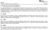
As some of you may know, the original xbox is really lacking in video output modes for the modern era. It is only capable of analog video out, and doesn't even support VGA through that.

Early versions of the xbox use a CX25871 as the video encoder, which can take a variety of digital inputs and in turn outputs analog video.
https://html.alldatasheet.com/html-pdf/153349/CONEXANT/CX25871/384/1/CX25871.html
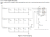
My suspicion is that the xbox uses the highest quality of these potential inputs, RGB24. If that turns out to be the case, I should be able to use the Texas Instruments TFP410 to turn these signals into DVI
https://www.ti.com/product/TFP410

End goal is to have a board with a BOM of under $20 that I can then install in my absurd stack of xboxen.

The catch: This is my first circuit design project and my first PCB design project, so I'm starting out way over my head. Wish me luck, I guess.
 

ttsgeb

.
Joined
Jan 19, 2016
Messages
97
Likes
154
upload_2020-4-3_19-57-1.png

I've gotten the majority of the wiring done, now for the hard parts that aren't just pin to pin wiring.

Those connectors on the right are just a direct copy of the pads on the V1 xbox motherboard to simplify wiring. It does mean there will be unused pads, but if you don't want to think about it, you can just wire from pad to pad in order and everything will be in the right place.
I do need the signal from one more pin, but I don't think I'm going to do the whole array of pads for that, because that just seems excessive. You can count your way to one pin.
 

ttsgeb

.
Joined
Jan 19, 2016
Messages
97
Likes
154
The board is designed and all the parts are on order, now we just get to see if my terrible board layout works worth a shit.


If this works, I'm definitely going to take some time to clean up the board a bit before the next run, I just don't really know what the hell I'm doing right now. Any tips are fully welcomed.
 

YveltalGriffin

First Wii U Trimmer
.
Joined
Jun 7, 2016
Messages
292
Likes
1,050
Location
South Florida
Portables
5
The DS for the TFP410 has a lot of helpful layout recommendations, including decoupling the various power supplies:
upload_2020-4-9_0-30-4.png upload_2020-4-9_0-34-8.png
The recommended decoupling cap networks are likely critical for a sensitive high-speed application like this.

DVI also uses differential signaling, so signal traces are paired up and length-matched.
upload_2020-4-9_0-45-17.png

My limited knowledge of diff pair routing says to minimize impedance discontinuities between paired signals, i.e. don't change layers for one trace and not the other, and keep the two paired traces as close as possible to each other. The DS also says to keep the four pairs as far away from each other as possible (to minimize crosstalk even more, I guess).

You probably wanna slap top and bottom ground planes onto the PCB, too. That'll help dissipate heat from the TFP401's thermal pad among other things. I think the DS's recommendation for a controlled-impedance 4-layer board is sensible considering it's a digital video application, but you can probably squeak by with two layers if you want to keep costs down.
 

ttsgeb

.
Joined
Jan 19, 2016
Messages
97
Likes
154
I expect my traces for the DVI to be complete shit on this revision, if I get shitty video quality, I'll cut a cable and solder it directly to the chip for testing purposes.
As far as the ground planes go, I basically just couldn't figure out how to make them work in KiCAD and I was being impatient to get *something* thrown together for proof of concept.

Thanks for the advice! I'll try to do better with Rev 2

UPDATE:
I've made some minor improvements to my board design. I still have a long way to go.
upload_2020-4-9_4-37-22.png
 
Last edited:

ttsgeb

.
Joined
Jan 19, 2016
Messages
97
Likes
154
Just noticed a silly error I made on the board design, so I've gone ahead and fixed that in KiCAD and need to remember to fix it when my boards come in the mail. Luckily I just need to solder in a short ass jumper to make the repair.
upload_2020-4-15_21-28-13.png

Now if only the boards could get through customs and get on their way to me.

EDIT: Decided I wanted to practice using KiCAD more and redid my board design to be more compact:
upload_2020-4-15_22-24-10.png
 
Last edited:

ttsgeb

.
Joined
Jan 19, 2016
Messages
97
Likes
154
I took a closer look at the xbox board for the first time today, and my base assumption was wrong.
The xbox does not use 24 bit single edged rgb, it likely uses 24 bit double edged rgb.
What this mean is that:
A) It uses half as many pins for video, so when I get something working the install will be significantly easier
B) The TFP410 almost definitely doesn't work for video, as it expects different signals at different points in the clock
upload_2020-4-17_8-22-18.png

C) I'll probably have to learn to use FPGAs
D) I might be able to sneak in HDMI compatibility
E) My boards that I'm waiting that were probably scrap to begin with are almost definitely scrap

I'm still going to throw one of the boards together and install it to see what I get, but I don't have high hopes for intelligible video from it.
 
Last edited:

ttsgeb

.
Joined
Jan 19, 2016
Messages
97
Likes
154
Welp, I've written the code to be able to use the TFP410 in my design, now I just have to figure out how to actually use it:
Code:
library IEEE;
use IEEE.std_logic_1164.all;
entity Splitter is
    port    (Clock                                                            : in    std_logic;
            P0, P1, P2, P3, P4, P5, P6, P7, P8, P9, P10, P11    : in    std_logic;
            R0, R1, R2, R3, R4, R5, R6, R7                            : out    std_logic;
            G0, G1, G2, G3, G4, G5, G6, G7                            : out    std_logic;
            B0, B1, B2, B3, B4, B5, B6, B7                            : out    std_logic);
end entity;
architecture Splitter_arch of Splitter is
    begin
  
        Splitter : process (Clock)
            begin
                if (Clock'event and Clock='1') then
                    R0 <= P1; R1 <= P2; R2 <= P3; R3 <= P7; R4 <= P8; R5 <= P9; R6 <= P10; R7 <= P11; G1 <= P0; G5 <= P4; G6 <= P5; G7 <= P6;
                end if;
                if (Clock'event and Clock='0') then
                    B0 <= P0; B1 <= P1; B2 <= P2; B3 <= P4; B4 <= P5; B5 <= P6; B6 <= P7; B7 <= P8; G0 <= P3; G2 <= P9; G3 <= P10; G4 <= P11;
                end if;
        end process;
      
end architecture;
entity ClockInverter is
    port    (Clock        : in std_logic;
            ClockOut    : out std_logic);
end entity;
architecture ClockInverter_arch of ClockInverter is
    begin
            ClockOut <= not Clock;
      
end architecture;
 

ttsgeb

.
Joined
Jan 19, 2016
Messages
97
Likes
154
upload_2020-5-2_7-32-44.png

I've done some board layout on the assumption that my program works and can be applied to the MAX V.

And don't worry, I flipped around the DVI connector to face the right way. :P
 
Last edited:

ttsgeb

.
Joined
Jan 19, 2016
Messages
97
Likes
154
geb.png

I've assembled my second prototype and have since cleaned up the solder bridges. I'm waiting on my programmer to arrive so I can hook it all up and see if it works.
 
Last edited by a moderator:

ttsgeb

.
Joined
Jan 19, 2016
Messages
97
Likes
154
Been trying to figure out why I couldn't program the Max V, the bent pins weren't helping, so I finally got around to fixing the chip, still didn't work... Caught the idea that maybe there's more to the JTAG interface than just putting pins there, and sure enough I need to put in a 10k pull up resistor on TMK and a 1k pull down resistor on TCK so when I wake up I'm gonna track down my resistor pack and bodge those in. Hopefully I'll be able to program the thing soon, and don't have to replace the Max V a fourth time. Regardless, there's another board revision in my future. One with everything on one side so JLC can assemble it and a couple of LEDs to let me know I'm getting the power I need.
 
Top