Hello everyone
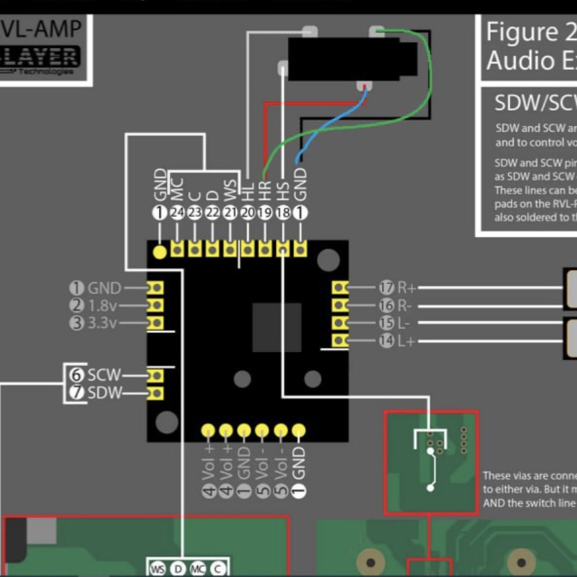
I was checking the connection between rvl-amp and headphone jack via ashida pcb with multimeter and I noticed that ground and right audio channel are swapped compared to the 4layer diagram. (The jack leg supposed to be wired to gnd is instead connected to hr and vice versa)
So I tested the jack pads below amp chip itself as a countercheck but I got the same result.
Just wondering why it doesn’t match the diagram. Does anybody know?
