penguin
.
- Joined
- Jan 16, 2020
- Messages
- 10
- Likes
- 10
Hi,
This post is just to document where I am up to and hopefully motivate to complete this project.
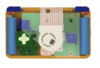
Just got an OMGWTF trim working this weekend WOOOOP")
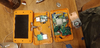
Photos


Cut with a multitool sanded with 120 grit sandpaper, then a high grit chisel sharpening block, edges of the Wii came out really smooth
Found 1.8v and 3.3v were directly shorted to ground so removed smd caps near the edges
But it was still shorting so I removed the LDO pins (This went horribly but I have some solder mask if I want to hide it)
This stopped the 1.8v short I think
Realised I sanded the edge of a cap near the PCB edge next to the nand chip after I removed this no shorts resistances attached for fun (I think the 1v to GND is wrong it was in the hundreds when I measured again when measuring with a multimeter all resistances seemed to change while measuring quickly at first then settled like the voltage while charging a capacitor)
Also while checking my wiring found I wired the U10 to wrong via

Using the original PMS as I bought all the PCBs a couple years ago
Theme
Super Mario Galaxy maybe
Design
Something simple (relative terms) like louii or maybe vertical design so basically a G-Boy
I like the ABXY as circular buttons rather than GC layout
Features
What comes with
RVL PMS
U-AMP
GC+2.0
Kingston adapter ( with a 128GB EVO Plus 3
Bluetooth if I can do the soldering
USBC PD (have some initial PCB plans that I made a while ago) although 4 layer tech's one is pretty cheap
Possible
MX chip
WIFI
USB-C PD

The PD bit is handled by an IP2721 or maybe a CH224K seems to be cheaper and more available to do the same thing (also doesn't require a transistor I think but I need to research)
Data multiplexing this is simple just connect USB to Wii when it sees 3.3v from PMS, but when it receives no voltage (off) the default connects USBC to the USB
Although as I designed this a year ago the specific chip has probably gone from digikey
The issue is powering the USB either have a 5v reg and a multiplexer (on this PCB I am designing) to switch power to the USB from the PMS or the reg.
or
Change the PMS code to have the PMS 5V regulator on when it is charging (this is the solution I want to do to minimise components needed but A code change will require a lot of research although do remember somebody's worklog doing this and B having the 5V reg on while charging my waste power but if I only use 5V for the USB it wouldn't be much.
Also designing differential traces seems to be quite specific although according the internet at USB full speed the traces don't need to be exactly the same length and vias are not too bad for data transfer rate
Future Plans
Attach a GC controller to test a game

Full cad design of case with PCBs
Test VGA
Test Audio (have some nice speakers out of laptop)
This post is just to document where I am up to and hopefully motivate to complete this project.
Just got an OMGWTF trim working this weekend WOOOOP
Photos
Cut with a multitool sanded with 120 grit sandpaper, then a high grit chisel sharpening block, edges of the Wii came out really smooth
Found 1.8v and 3.3v were directly shorted to ground so removed smd caps near the edges
But it was still shorting so I removed the LDO pins (This went horribly but I have some solder mask if I want to hide it)
This stopped the 1.8v short I think
Realised I sanded the edge of a cap near the PCB edge next to the nand chip after I removed this no shorts
resistances attached for fun (I think the 1v to GND is wrong it was in the hundreds when I measured again when measuring with a multimeter all resistances seemed to change while measuring quickly at first then settled like the voltage while charging a capacitor)Also while checking my wiring found I wired the U10 to wrong via
Using the original PMS as I bought all the PCBs a couple years ago
Theme
Super Mario Galaxy maybe
Design
Something simple (relative terms) like louii or maybe vertical design so basically a G-Boy
I like the ABXY as circular buttons rather than GC layout
Features
What comes with
RVL PMS
U-AMP
GC+2.0
Kingston adapter ( with a 128GB EVO Plus 3
Bluetooth if I can do the soldering
USBC PD (have some initial PCB plans that I made a while ago) although 4 layer tech's one is pretty cheap
Possible
MX chip
WIFI
USB-C PD
The PD bit is handled by an IP2721 or maybe a CH224K seems to be cheaper and more available to do the same thing (also doesn't require a transistor I think but I need to research)
Data multiplexing this is simple just connect USB to Wii when it sees 3.3v from PMS, but when it receives no voltage (off) the default connects USBC to the USB
Although as I designed this a year ago the specific chip has probably gone from digikey
The issue is powering the USB either have a 5v reg and a multiplexer (on this PCB I am designing) to switch power to the USB from the PMS or the reg.
or
Change the PMS code to have the PMS 5V regulator on when it is charging (this is the solution I want to do to minimise components needed but A code change will require a lot of research although do remember somebody's worklog doing this and B having the 5V reg on while charging my waste power but if I only use 5V for the USB it wouldn't be much.
Also designing differential traces seems to be quite specific although according the internet at USB full speed the traces don't need to be exactly the same length and vias are not too bad for data transfer rate
Future Plans
Attach a GC controller to test a game
Full cad design of case with PCBs
Test VGA
Test Audio (have some nice speakers out of laptop)