Worklog OpeN64 - Worklog

  • Thread starter Thread starter cy
  • Start date Start date

cy

.
Joined
Sep 3, 2020
Messages
389
Likes
882
Portables
8
This project has been completed and can be found here.

Alrighty, I've kept this under wraps for long enough. For the past couple of months, I've been working on and off (mostly off) on a project I've been calling "OpeN64". This project aims to recreate ALL functionality of the original Nintendo 64 motherboard. This essentially means making a motherboard that will behave EXACTLY like the original N64 motherboard and have room for ALL of it's original components so you can relocate everything from an original board onto it.

As of right now, I'm only aiming to recreate an 03 revision motherboard since that board supports the RAM swap. To do so, I've been utilizing the Inside Gadgets N64 motherboard scan that was posted to the N64 compendium a while back. In order to achieve all of this, I want to move one step at a time and recreate a trimmed N64 motherboard first so I'll be able to populate that and hopefully improve my time trying to troubleshoot this project in the event that it doesn't work. Only after I have successfully recreated and stress tested a trimmed N64 motherboard will I move on to adding the remaining voltage regulators, and other critical components a normal unmodified N64 has.

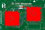
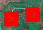
No, this isn't an April fools joke. I'm genuinely serious about this project! To prove that, here are a few screenshots of the work I've done in CAD:
OpeN641.png


The schematic is unfinished right now. Really, I've been trying to start by making symbols for the major components, making all the connections in the schematic, and then making those same connections in KiCAD's PCB Editor. This may not be the best practice, but it makes the tedium of this project a lot more tolerable.

OpeN2.png


I wasn't able to get all the components on screen for this screenshot, but I think you get the idea.

@Y2K Was suggesting I use a better naming schematic that labels the function of each trace. I'm willing to do that, but documentation on each line's functionality is limited, and I'm not an electrical engineer. With that said, Y2K gave me a few diagrams and a solid path forward to better documenting the RCP lines myself, so stay tuned!

Here's a shot of it from the 3d preview for good measure.

OpeN3.png


A lot of these components in the PCB editor don't even have schematic data for them yet. I kind of just went crazy making footprints one day and today I decided to rearrange them just to get an idea of what progress for this project was looking like. I'd say all in all, it's coming along really well! At least the front is anyway! I haven't started making ANY connections for any components that don't yet have a schematic. Really, the extra footprint placements are just a mock up so I can get a better idea of how my progress is coming along.

Right now what I want from the community is feedback or suggestions on how I can make this project better. Remember that as of right now, my main focus is NOT to recreate the ENTIRE motherboard for historical purposes or to try and make an 1:1 copy of it aesthetically and visually. My goal with this project it to copy it's functionality electronically meaning my goal for now is just to make it function. Once I have a stable and functional motherboard that electronically recreates the N64's functionality to the best of my ability, we can look into possibly making it look the same aesthetically (I.E. 100% identical trace routing, silk screen, etc). I'm not certain that I'm willing to go that far with this project however. I think that recreating everything the best I can so that every component can be relocated from an original N64 board and made functional is what matters, at least for now.

I'd like to thank @YveltalGriffin @Y2K @cheese and @thedrew for giving me help and feedback on this project already. Of course I'm not anywhere near finished, but you guys have given me an outstanding starting point for this!
 
Last edited:
Love seeing these recreation projects! Great way to salvage damaged and corroded systems and make some tidy functional units out of them
 
Love seeing these recreation projects! Great way to salvage damaged and corroded systems and make some tidy functional units out of them
Thank you! I won't lie though, the primary intention with this project is definitely an N64 AIO. A fully open sourced N64 motherboard isn't going to be much extra work after I get a simulated trim working though, so I figured I may as well go all the way with it. 75% of the work will already be done anyways.
 
It's been a month and a half and I've done almost nothing on this project. I was waiting on someone to do a Rev 3 motherboard scan for me, but after waiting for over a month and a half, that still hasn't happened. I'm not mad or trying to call anyone out or anything, it's been a weird and complicated mess though, and I'm hoping we end up with proper scans eventually. If not, I'll just get a decent quality scanner and take some scans of my own.

All that aside, I've gone ahead and renamed a bunch of the lines I had in my schematic to be more in line with what they actually do:

RCP:
RCP.png

CPU:
CPU.png

RAM:
RAM.png


I've added a few additional components to the schematic since last posting about this too. Here's what it's looking like now:
Schematic.png


I've noticed that I seem to be running out of space. I'm not certain if there's a way to fix that and re-scale the workspace, but I have run into a wall once or twice that limits how far I can go in a given direction. I'm assuming this can easily be fixed, and if it becomes more of a problem I'll probably research it and find whatever it is I'm running into.

On another note, I've found a temporary workaround for not having proper board scans:

UV Light 2.png


This is from a UV light I purchases for curing solder mask that I bought for a different project. I found that it was strong enough to help me easily see where and how the traces are routed on the board. This is critical for knowing how all the capacitors and resistors are routed as there's a ton of silk screen that obstructs them in the more densely packed areas. This trick also works with my phone's flashlight, but I'll have to use something else if I want to be able to light one end of the board and take a picture of the opposite end.

The RCP, CPU, RAM, and Disk Drive expansion slot do block some of the light as do a few caps and other components. Luckily, the trim I messed up for my initial Cyxty Four build is working as a wonderful sacrifice! Before I even started this project I had removed the RAM, CPU, and RCP, I'll have nothing to lose by removing a few other components from it.

Here's how that looks with my new light trick:
N64 RCP.png


I've got a few stray wires and various components on the board still, but this is going to help a lot with making a proper schematic and properly routing things on the board in the PCB editor.

This trick is by no means a replacement for a full proper board scan, but it should be enough to move me past the finish line for this project in the off chance that those 03 board scans never end up happening.

The final thing I'll share is some of the Compendium work I've done. There's still a lot to do before I make this into a proper compendium, and honestly, making a full on compendium was never one of my goals with this project (this project alone will kind of act as a compendium in a lot of ways). It certainly won't happen unless and until we have proper board scans of this layer and the copper layer of this mobo revision. Even then I'm not certain I'll want to make a complete one. This one I'm working on now is really just being used as a guide to help me verify my work.
compendium.png


I'd like to thank @Y2K for helping me enable a proper dark theme for the schematic and symbol editors, and @YveltalGriffin for further advice on making this project a reality. I'd also like to thank @thedrew for giving me advice and feedback on what I've done so far. I'm hoping to get more work done on this project soon.
 
It's been a month and a half and I've done almost nothing on this project. I was waiting on someone to do a Rev 3 motherboard scan for me, but after waiting for over a month and a half, that still hasn't happened. I'm not mad or trying to call anyone out or anything, it's been a weird and complicated mess though, and I'm hoping we end up with proper scans eventually. If not, I'll just get a decent quality scanner and take some scans of my own.

My fault OG

1747402386718.png
 
It's been quite some time since I've worked on this. I kind of lost motivation to work on this project while I was waiting for the board scans from either @CrazyGadget or @YveltalGriffin , not trying to throw shade or anything, just kind of how things played out. Anyway, I recently got the motivation to resume work on this.

I was talking to @cheese about this project one night, and he was suggesting I finish the compendium I started on this board revision. Initially I disagreed with him because it seemed like a ton of extra work that wouldn't really be necessary or helpful. I had some more time to think about what he said though, and I realized he was probably right on the money. When I started working on the schematic for this, I found it was difficult to follow and figure out exactly where each connection went. This was my initial reasoning for wanting board scans that included a sanded away solder mask and silk screen. I'm realizing now though what I really need is a compendium of this board using said scans.

Before anyone mentions it, yes, I am aware that ShockSlayer already made an N64 compendium. The rev 9 board his compendium is based off of is wildly different though, and doesn't support RAM swapping and has worse potential for RGB video modding. This board revision that I'm making mine on should cover most of the earlier revision boards based on the research and board comparisons I've done. Don't get me wrong, ShockSlayer's N64 compendium has helped me a ton in the past (I'm looking at you RCP wiring...), but it has fallen short when covering earlier board revisions -- it also lacks the exposed copper layers I've been working with (again, thanks to @CrazyGadget <3).

So with all that, here's a small but meaningful update to this project:

1755323653126.webp


Until this compendium is finished, I don't expect to do any more work on the OpeN64 project itself. The way I look at it though, this is all part of the process. This will only serve to further the N64's documentation, and it'll make a wonderful edition to the OpeN64's github repository.
 

Attachments

  • 1755313507304.webp
    1755313507304.webp
    90.3 KB · Views: 69
  • 1755313801338.webp
    1755313801338.webp
    120.2 KB · Views: 88
Last edited:
The front of the compendium is mostly finished. I've still got a number of lines to trace on the right side of the board, but I'm opting to hold off on those until I get most of the back traced since the lines I'm yet to trace all go to the back.

Here's how the front is looking:
1756176055322.webp


I've only just begun working on the ground plane for the back, but here it is anyways:
1756176298900.webp

(This will be flipped in the final release for the sake of making everything easier to follow)

This compendium has been a big project on it's own and has already helped me to repair a broken motherboard I got online. I'm looking forward to releasing this to the community as I'm sure it'll be a great resource!
 
The compendium is more or less finished now:
1756793973977.webp
1756793994295.webp


I still have some basic work to do so the final result is polished up nicely and provides a better user experience, so this won't be released for a little while. The traces and planes have all been mapped out though. Once I've gotten feedback from Shank and polish this up, I'll talk to Cheese about getting it posted officially, and I'll link that post here once it is made.

For now though this is gonna be a great reference to help me build the schematic for the OpeN64.

Edit:
The compendium has been released and can be found here.
 
Last edited:
It's been a bit since I've posted an update, so I'll give a brief update of my progress here:

1758389767234.webp


I've gotten started on replacing my tags with wires here, and while I haven't gotten a ton done yet, I have at least finished making up all the symbols:

1758389893295.webp


I plan on splitting this up into multiple sheets once I have the video circuitry done.

I also have most of the footprints made up, although I kind of have had most of those covered for a while now. Once the schematic is finished, I'll go back and double check my footprints to verify I have everything accounted for. After that, it should just be a matter of linking the symbols to the footprints and then manually recreating everything from there. That last part may sound like a lot of work, but I don't think it'll be too bad since the motherboard scans will act as a checklist making the work a bit more mindless.

Right now I need to find the motivation to work on the schematic. After I finished up the compendium, I kind of lost the motivation to work on this. I want to get this project completely finished within the next month or two so I can get the boards ordered up and assemble everything for testing, but I'm still looking for the motivation to continue this, so we'll see.

One final thing I will say here is that the compendium has been published and I updated my previous post to reflect this as promised. So feel free to check it out if you have any interest or use for it. I'm hoping people find it useful!
 
It's time for a mini update. The AVE section has mostly been mapped out now on the schematic:

1759744312057.webp


This schematic has been a lot less work than I was expecting. I know I've still got quite a bit to do, and I've been moving at a snail's pace because I haven't had the motivation, but this really hasn't been difficult at all. It's been rather quick too since I really haven't put much effort in since my last update, and I'm already mostly finished with this sizable section.

I've made a few small changes to the RCP, RAM, Cart Slot, CPU, etc and I've added the RAM expansion port:

1759744590215.webp


Originally I had this mapped out with just labels because I had no idea what I was doing, but I've got a much better understanding of how schematics are supposed to be made now, and I'll be replacing most of the labels here with wires. I'll also be cutting and pasting these components to a completely separate sheet to keep things neat.

One thing that won't be changing though is most of the labels I've got on the right side of the RCP, and the left side of video components like this:

1759744972913.webp
1759744930439.webp


This is because these components will be on different sheets from each other, and this will be the only way to connect them across sheets.

Something else I'll mention here is that I've started focusing on copying RDC's N64 Rev03/04 schematic rather than verifying everything via my compendium. This is because when I do eventually go into the PCB editor to place the components and make the connections, I'll be using the board scans provided by @CrazyGadget as a reference to ensure everything is as close as possible to the original board. So if RDC's schematics end up being inaccurate at all, it'll show in the scans. This is gonna save me from having to manually verify every connection either via multi-meter or by constantly alt-tabbing in and out of my compendium. And of course, I'll absolutely credit RDC for the schematics since they've been so helpful!

So yeah, the plan from here is as follows:
Finish the schematic > Finish any remaining footprints > Start mapping out the entire board in the PCB editor > Correct any errors I encounter along the way by updating the schematic.

If all goes according to plan, I'm hoping to have all the CAD work finished by the end of this month. This is mainly since I'd love to get the PCBs ordered and shipped sooner rather than later so I'll have extra time to troubleshoot. Really, my end goal with this project is to have it done before the end of the year.
 
Time for another update! I got most of the schematic together, and I decided it was best to start putting the PCB together so I could use it as a checklist for the few remaining things left over on the schematic:

1760628434121.webp

1760628453869.webp


It might not look like much has been done on the PCB end of things, but I actually restarted the trace work I had done before this. Unfortunately, I've been having issues with KiCAD crashing whenever I use the Router Highlight mode in the PCB editor, so I've been having to rely on the line tool which allows for DRC violations more easily. Not at all ideal, but I can't change the fact that KiCAD still doesn't want to officially support Wayland on Linux.

That said, this is looking pretty darn good! Originally I started drawing polygons for the ground planes, but I was told that I should be able to auto fill it with a ground pour once all the traces are routed correctly. I may still use polygons to isolate the 3.3v pours, and honestly, I'm a bit skeptical about relying on ground pours for this project, but I'll give it a try once everything is mapped out since it'll definitely save a ton of time and hassle.

I was originally going to show the completed schematics here, but this is kind of where this project takes an annoying and frustrating turn. @Xenii contacted me asking for the footprints being used for some components here, and I was happy to provide them. But not too long after that, he informed me that my schematic making process was being done wrong. This is something I would've rather learned before making the schematic rather than after finishing it because I effectively wasted my time creating the original one.

Now, I was aware of the discrepancies between my schematic and the RDC schematics, but I was assuming that was more of a preference thing and less of an "this is unreadable by most" kind of thing. And honestly, my schematics were more readable to me than the RDC ones are. The other half of this is that I already had my symbols made by the time I started looking at the RDC schematics, I was assuming what I had was fine since no one said anything, but I wish I would've been less of a free thinker here and just copied RDC.

Anyways, I do have access to some sacred texts now that I didn't have before starting this project, so while remaking the schematic is gonna be a frustrating and lengthy setback, I can at least base it off of something... a bit more authentic which is very much in the spirit of this project!

So with that, I went back to the drawing board editing my symbols to be just right...

1760629103911.webp
1760629146645.webp
1760629172788.webp
1760629186769.webp
1760629200181.webp


These aren't all the symbols I've redone, but it should give an idea of where this project is now headed. @Xenii Was extremely kind and helpful in DMs and offered to fix some questionable things in my footprints as well as offering to help with making new symbols for the RCP, CPU, and RAM. He's working on a similar project right now, and due to the similarities in our projects, it made sense for us to work together a bit with this.

I still need to evaluate and sanity check the changes he made to my footprints - since, mine are based off board scans, and his changes are based off the logic that standard pin spacing should be following. This isn't to say I don't trust his judgement, I just want to be certain that the pin spacing is correct, so I'm planning on printing them out on a sheet of paper and testing against the real components removed from a real N64.

This might not seem like much of an update, but I've put many hours of work into this project since my last update, so I figured this was a good time to keep people informed on the latest. At this point, I'm not expecting to have the CAD work for this project finished before the end of this month. I've got a road trip I'll be going on soon, and I'm starting to feel burned out. Finding out my schematic wasn't very good certainly wasn't very motivating either. I'm hoping I can still have this project finished before the end of the year, but we'll see. I want to enjoy the time I've taken off, I've made a lot of new friends recently, and I can definitely see myself choosing to spend time with them over this project.

I would like to thank @Xenii SO SO much again for helping with this project! He's helping to save a lot of time and hassle, while also making the results better overall! Thank you so much again man! Will definitely save a spot for your name on the final board!
 
Will this open the door for manufacturers to start building 64 boards? Will you make boards to sell? @cy
 
  • Like
Reactions: cy
Will this open the door for manufacturers to start building 64 boards? Will you make boards to sell? @cy
This project is going to be open source, so if people want to start building custom N64 boards using this as a base, nothing would stop that. I won't be making boards to sell for this project, no. The main goal here is just to provide the community and the internet at large with a "good enough" N64 motherboard design.

If someone wants to use this project as a base, then by all means they'll be able to. I just want others and myself to have a solid and known good/working start point for an N64 AIO type board.

This project has been on hiatus for a bit due to personal reasons, but I'm hoping to finish it sometime over the summer this year (or sooner if I have the time).
 
Really nice project. I am looking to modify a repro of the original N64 motherboard in order to substitute the Composite/S-video output with an HDMI output. In other words, I want to create a N64 motherboard compatible with the original case, but with the HDMI mod included in the motherboard instead of the Composite/S-Video output. I would like to know where I can download the files in order to modify them. Thank you.
 
Really nice project. I am looking to modify a repro of the original N64 motherboard in order to substitute the Composite/S-video output with an HDMI output. In other words, I want to create a N64 motherboard compatible with the original case, but with the HDMI mod included in the motherboard instead of the Composite/S-Video output. I would like to know where I can download the files in order to modify them. Thank you.
Funny you mention this, I thought this would be a great use-case for this project!

Having said that, this project is unfinished right now, and the current progress on it isn't far enough along for release to allow for something like this. I started working on this again tonight, but expect my progress to be slow since I've been stupid busy with college classes.

I'm planning on hitting this project hard after my 8 week accounting class is over since that's been taking up all of my free time lately.
 
It's been a while since I've posted a progress update. I didn't realize I had made as much progress as I have since the last post, so here's an update:

1770003141969.webp


The schematic is coming along rather well. I want to say it's around 70% of the way there. It's difficult measure my progress, but I eye balled my schematic and the official schematic side by side, and I'm not seeing a ton of things left to do on mine which is definitely a good sign!

I would share what I'm talking about so you guys could see for yourselves, but I don't want to share anything relating to the official schematic for legal reasons.

Probably more updates coming in February, and probably lots of major updates coming in March.
 
After doing a bit more digging and looking a bit more closely at the schematic, it looks like I overestimated how much there was left to do.

As far as I can tell, right now the first real draft of this schematic is done:

Screenshot_20260203_224820.webp


I've compared my schematic with the official schematic quite extensively though, and I can safely say that anything unaccounted for on mine is almost certainly a minor detail. There definitely could be a missing resistor, capacitor, or other small component that's easy to miss, and if that's the case, I'll inevitably end up finding it when I design the board.

Realistically speaking, right now it makes the most sense for me to shift my focus to board design seeing how that's going to act as a sanity checker for my schematic.

Speaking of, here's what my current progress is looking like on the board:

1770177773047.webp


1770177799742.webp


I haven't made any real updates to this yet since updating the schematic. I know I'll need to assign footprints, update the PCB from the schematic, and do a whole slew of other things before I really get to working on this.

So I guess the TLDR of this update is that the schematic is essentially done, I just need to get to work on placing components, routing traces, updating the PCB from the schematic, etc.

I'll close this update by saying that my college classes this semester have been extremely disrespectful of my free time and have been absolutely killing me. This could be the last update for this entire month due to how egregious college have been. Realistically speaking, I shouldn't even really be working on this project right now, I should probably be relaxing instead. But I guess working on this is it's own form of relaxing seeing how it's satisfying to watch my work come together.
 
So I'm continuing to work away because I still have the motivation somehow. Would be really cool to get this done in time for MGC, but that's very unlikely. Anyways, here's how the board is looking:

1770445964859.webp

1770445980971.webp


A lot has been added. I've initially chosen to make vias my main focus due to how safe of a choice they are to work on. I've added a good number of traces though, and it's safe to say this project is starting to look like an N64.

I'm faced with a bit of a problem now though. I've been using polygons to draw out various planes, and while I want to just use a proper filled zone for the ground plane, I'm a bit worried that it won't come out quite right. Still, it's extremely difficult to justify making polygons for the ground plane, so I think I'll use a filled zone for the ground plane, and polygons for the voltage planes. I'll need to add copper to some areas of the automatically generated filled zone for the ground plane, but I'm hoping it'll still save me the time of trying to manually trace out the ground plane.

I would do the same with voltage planes, but I'm expecting I'll need to add copper to parts of them for them to come out properly. This screenshot provides an example of why:

1770446330297.webp


This is the VTERM plane, and inside it is a GND plane. I'm really not liking how some aspects of this are being managed. I could make changes to it by adding traces, polygons, or whatever have you, but I want to try to keep this board as close to the original as possible (within reason) and this just isn't doing it for me. I'm going to keep kicking around ideas, but I don't know that using filled zones for all of my voltage and other planes is going to be the answer.

Maybe the answer really is to just alter the filled planes with extra polygons to patch up what I don't like, IDK.
 
I'm really not liking how some aspects of this are being managed.
I suppose what you don't like is how the pads are connected to the planes with just a small trace?

Try right-clicking the pad, go to the "Connections" tab and change the "Pad connection" setting from "Thermal relief" to "Solid" and regenerate the plane. It should make the pad part of the entire plane, without cutouts.
 
  • Like
Reactions: cy
I suppose what you don't like is how the pads are connected to the planes with just a small trace?

Try right-clicking the pad, go to the "Connections" tab and change the "Pad connection" setting from "Thermal relief" to "Solid" and regenerate the plane. It should make the pad part of the entire plane, without cutouts.
Yeah, that's what it was. Someone in the BitBuilt Discord was able to help me resolve this when I was going over ground plane connections. It's exactly what you said it'd be though so I appreciate the help!

It's been a little since I posted an update here, so here's where I'm at:
1770774115574.webp

I'm not gonna pretend that the front here is completely finished. But it's pretty clear that the majority of it is done now. There are a number of missing traces that go to vias on the other side of the board, and for the sake of making this easier to route, I'm saving those for after I finish populating the back side.

Speaking of:
1770774214223.webp


There's really not a ton done on the back right now, but this is a start at the very least, so there's that. I'm recognizing that the majority of the work that'll be done on the back is going to be placing components. Stuff like this is what @CrazyGadget 's board scans are gonna help a ton with! My own work from the compendium I made has been helping out a ton too.

I'm not sure how much more of this I'll be doing this month. My accelerated accounting class is still hitting like a truck, and my other classes have also been demanding an unfair amount of my time. My accounting class ends Saturday of next month though, so I'm hoping after that I'll have time to finish, order, and assemble this project.
 
Back
Top