
You are using an out of date browser. It may not display this or other websites correctly.
You should upgrade or use an alternative browser.
You should upgrade or use an alternative browser.
Completed [2026 Summer contest] GBAWii4 & Wii Pico, a redesigned Wii motherboard in a GBA Cartridge
- Thread starter RoseDagger
- Start date


- Joined
- May 29, 2026
- Messages
- 24
- Likes
- 37
- Portables
- If you can carry it, it's portable.
This is absolutely insane (in the best way possible). I'm excited to see the final result.

- Joined
- Sep 27, 2025
- Messages
- 74
- Likes
- 50
Welp, congrats, you got my vote lol

- Joined
- Jan 15, 2021
- Messages
- 68
- Likes
- 267
- Portables
- Wii PICO (Complete), Wii Zero (WIP), GBAWii4 (WIP), GB Adwiince v3 Revenge (On Hold), GB Adwiince v2 (Dead)
Heya! Update four here we go! (Spoiler the PICO boards arrived! ^^ )
Quite a bit has happened since last time! First off after some back and forth I decided to make a version where the tracks were straight and not length matched. Primary reason being that skew would not be large enough to matter anyways, and it would let me spread some of the traces further apart to limit cross coupling.
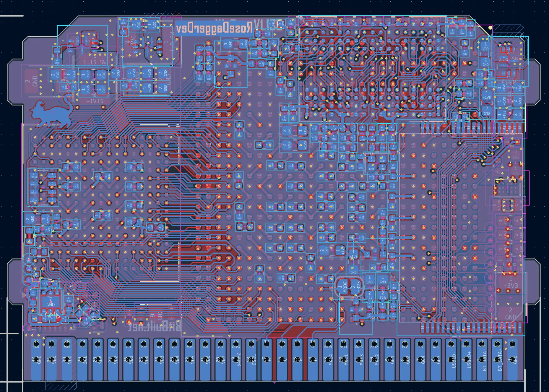
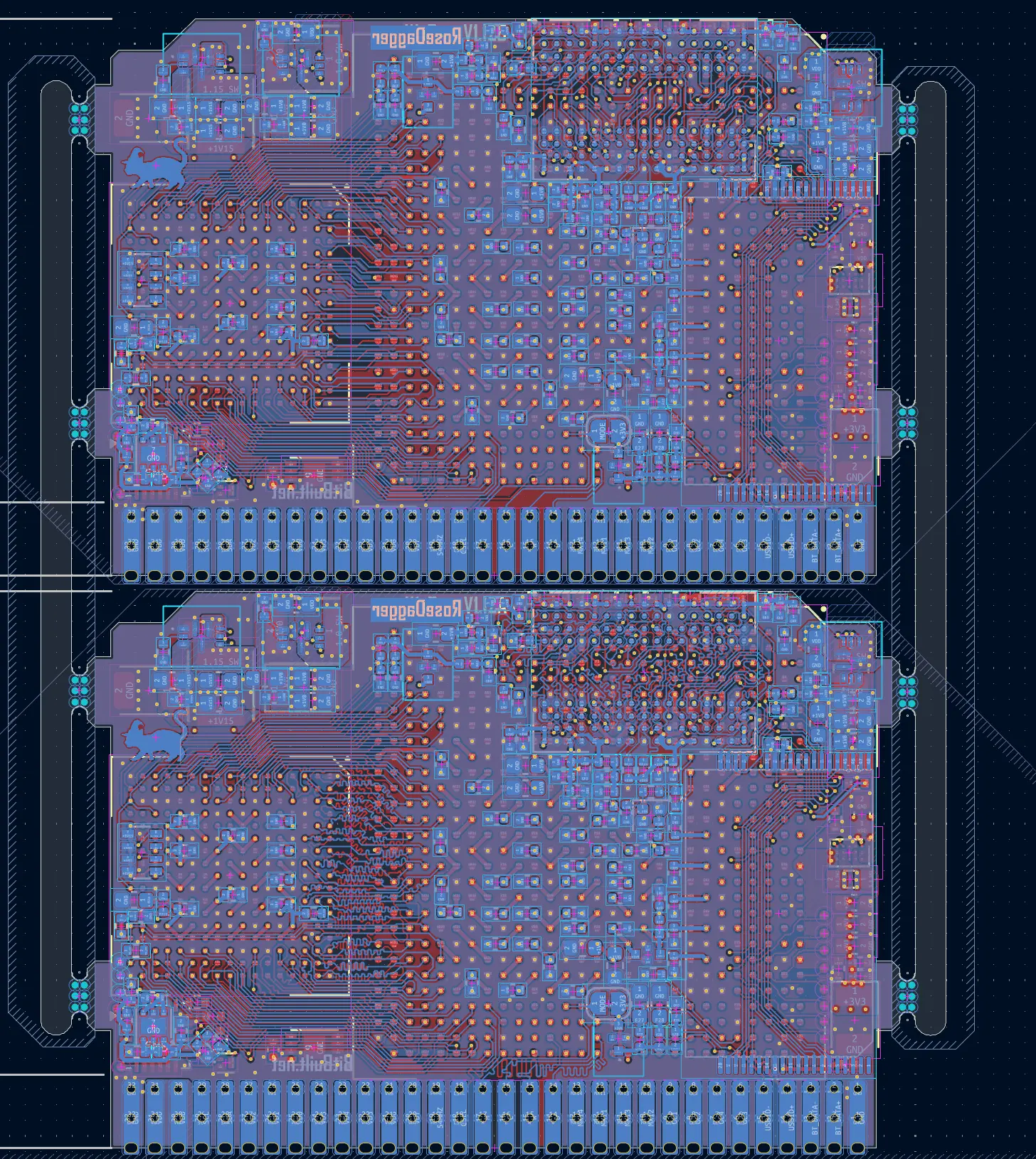
However, being stubborn and not wanting to admit all the time I spent length matching was a waste, decided to just make a panel with both the length matched traces, and the straight traces, so that I could test both XP
I’ll include a detour into impedance matching, that turned out to be irrelevant, and can be skipped if you don’t care XP
So, I felt ready to order, I had triple checked everything. Made both a length matched version and a straight version (during pride I know XP ), and made my own panel. I checked the design against the DFM tool for JLC, the uploaded the design and toggled all the important settings:
- 6 layer board
- 0.8mm board thickness
- 2oz copper
- The smallest vias JLC allows 0.15mm
- Castellated edges
- Color Purple!
And saw with dread how every option increased the price... But I decided to bite the bullet anyway!
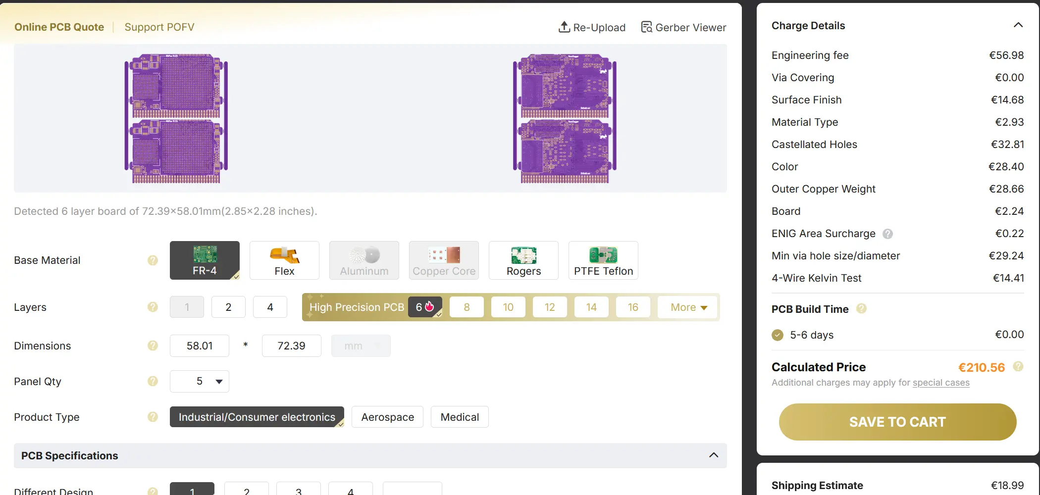
JLC says their review should take between 10min to an hour… An hour came and went… Then two… I checked when they were supposed to be open, and they are supposedly running 24h during weekdays. So, I keep waiting, trying to busy myself with other things... It’s a complex circuit, it’s no wonder it is taking extra time… At the five and a half hours mark it finally went through, whoop! They up charged me more for the panel but otherwise seemed like I was in the clear, double whoop! So, I paid and went to sleep in the knowledge that everything would be fine.
Foreshadowing is a literary device...
Anyway... The next morning, I saw I had an email from their techs... telling me that with the 2oz copper I had ordered, I no longer met their minimums. This was apparently not caught in their initial review… I talked it out a bit on the discord before deciding to print a test print on 1oz instead and remove all the expensive options I could to bring the cost down.
So, I got rid of the panel, only ordering the straight ( :/ ) trace version, in 1oz copper, in boring green, and without castellated edges. It got the cost way down, and would make it easier to do a reprint in case I'm not a goddess of perfection XP , and there were any issues which slipped by.
Then in intensely waited for a week till the boards arrived on Thursday XP
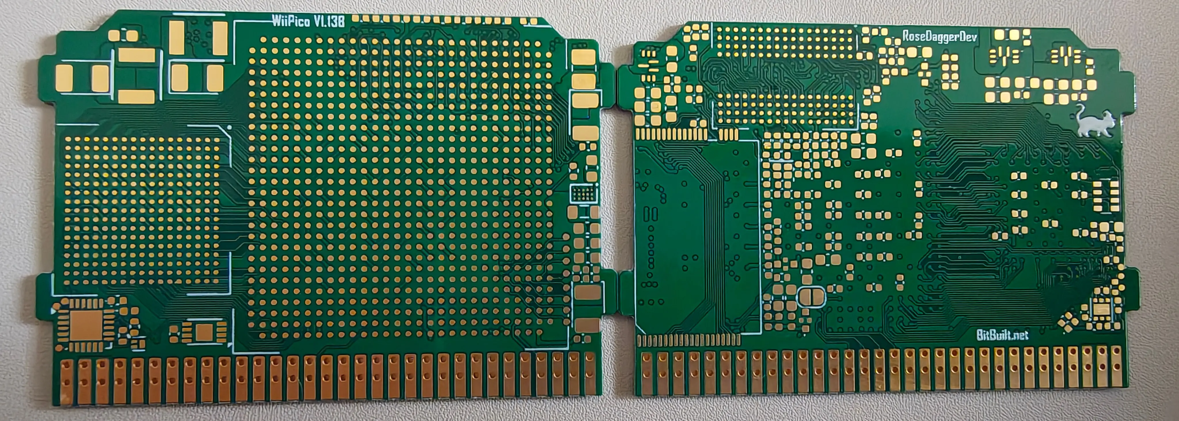
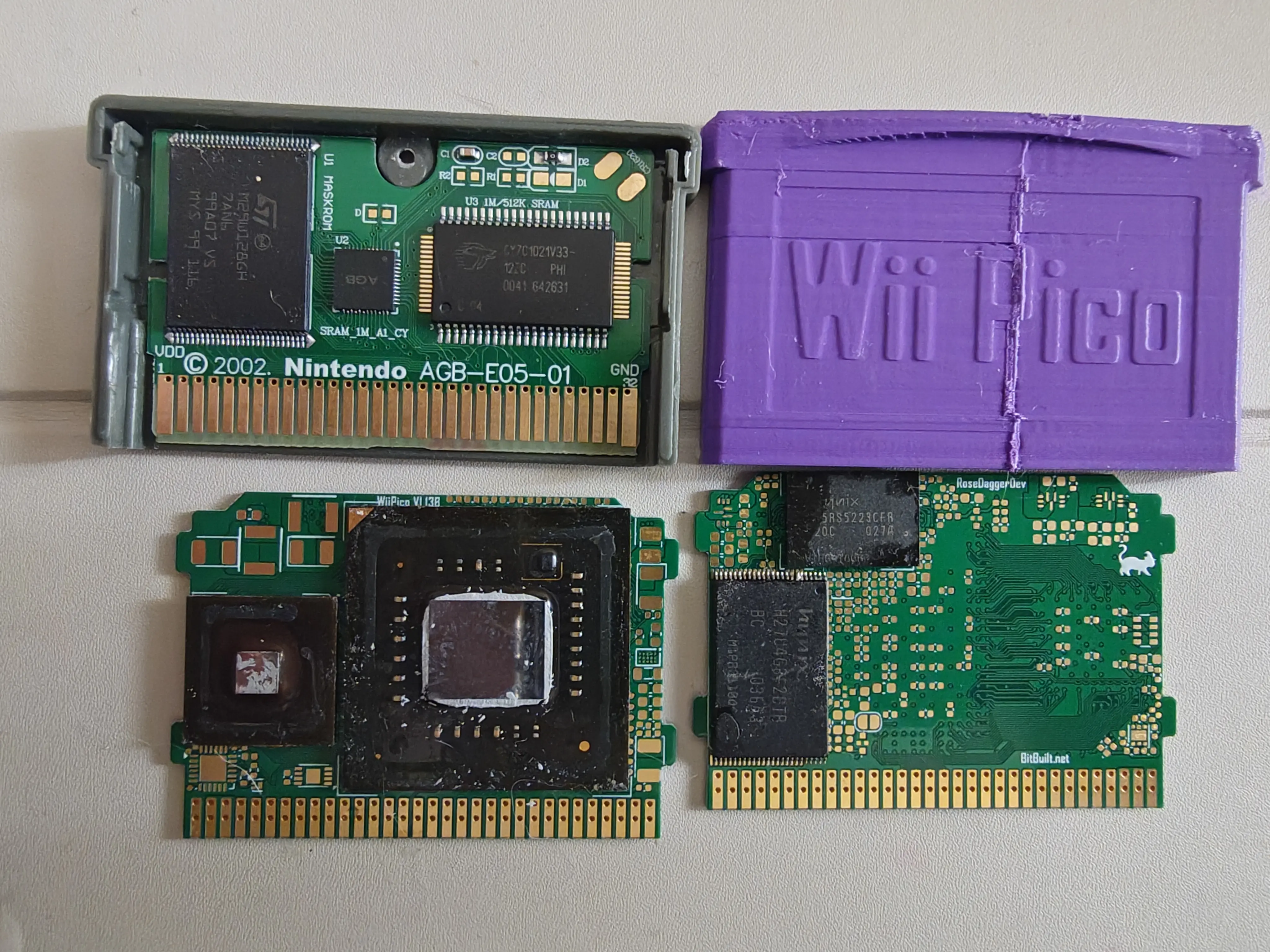
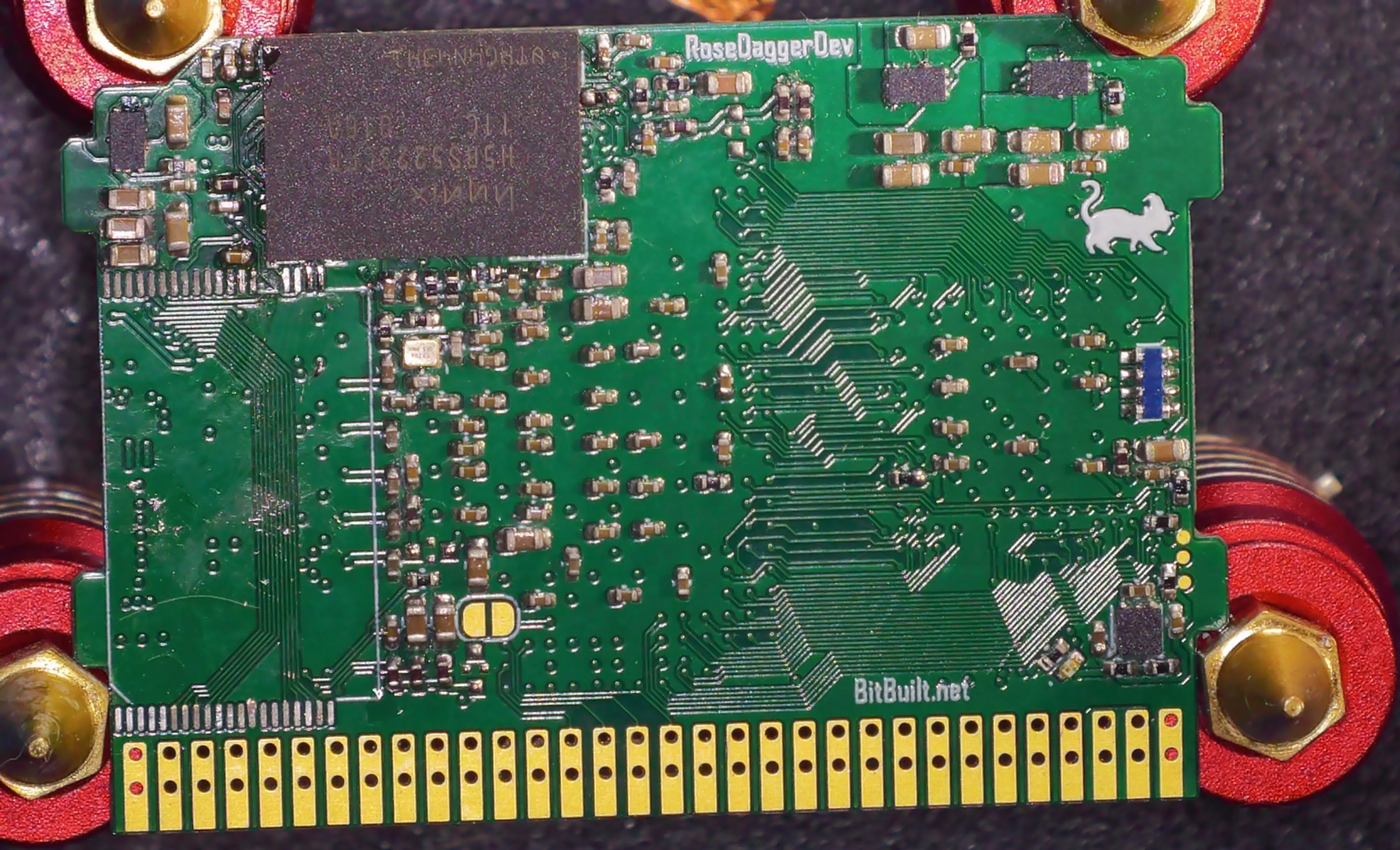
They are kinda scary small the PICO is! And it turned out quite well even if it isn't purple ^^ Though I missed out on putting “2026 Nintendo AGB-RVL-01” on the bottom silk screen. But maybe for a second print if I needed it.
This weekend I started soldering, focusing on the back. However, I discovered that I had ordered the wrong feedthrough caps, ordering 100pF instead if 1uF. I have no clue how I picked the wrong size that badly... So got to make another order and get the right ones this time. Good thing I almost never make mistakes XP
I had planned to be stubborn and just use the regular Hollywood 1 from the regular wii I just got for this. However I was convinced on the discord to not be stupid and to just order a Mini so I can get better thermals and better undervolting. Thanks everyone ^^ And thanks to flux_sniffer for helping me on how to source the correct mini version ^^
As for the actual reballing process… Lining up the balls is fine, but getting them to melt into place without moving using hot air is kinda a pain. So I decided to cheat XP I decided to try and build an IR top heater so that I could melt the balls into place without hot air. I found a guide, the components, some aluminum extrusions to make a thing to hold it, ordered everything, and felt quite clever about myself finding a way to avoid doing something really difficult XP And I do a lot of smd soldering so it felt like an investment regardless, just putting my boards under the IR top heater to melt everything all at once as if I were baking the board.
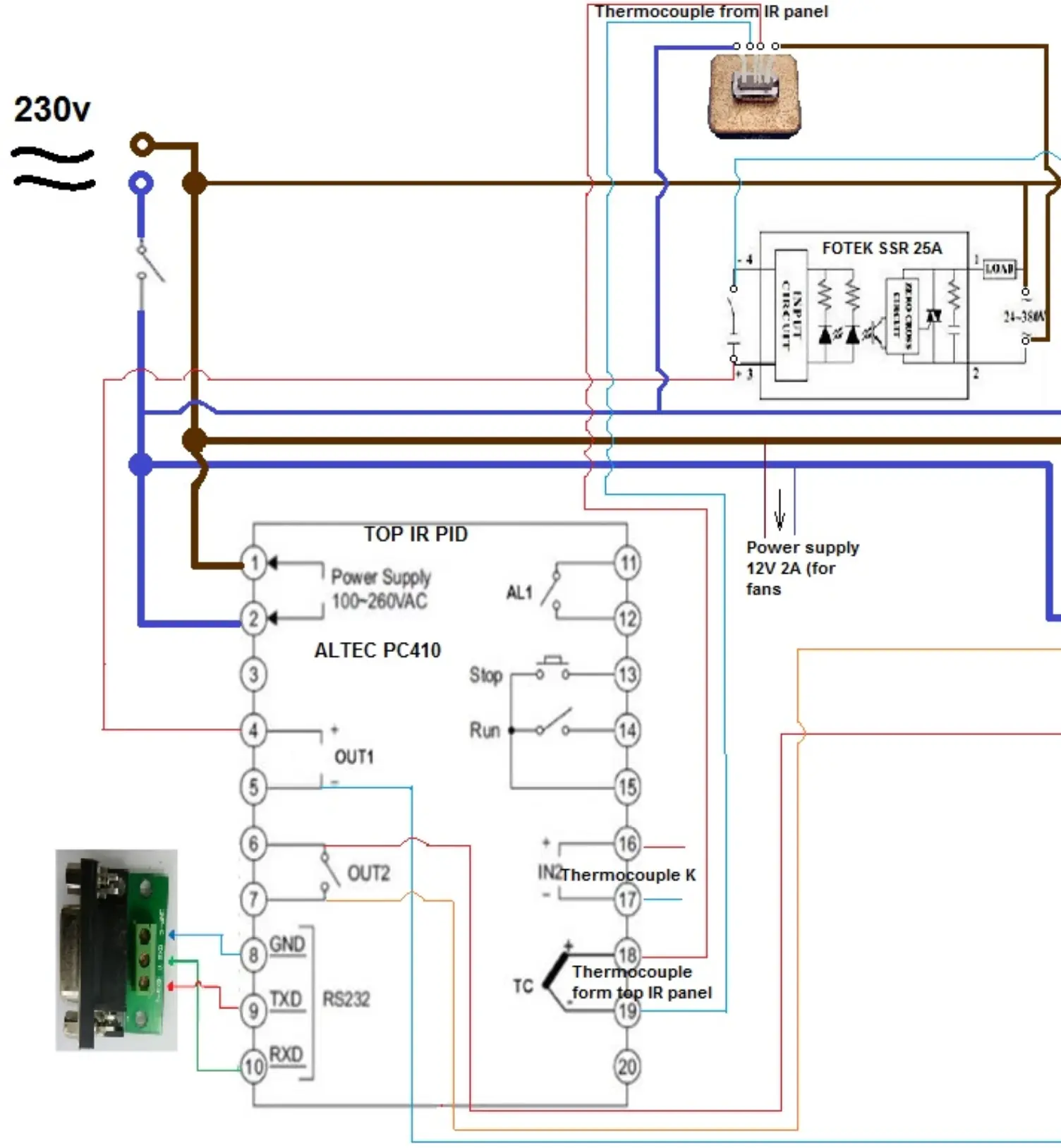
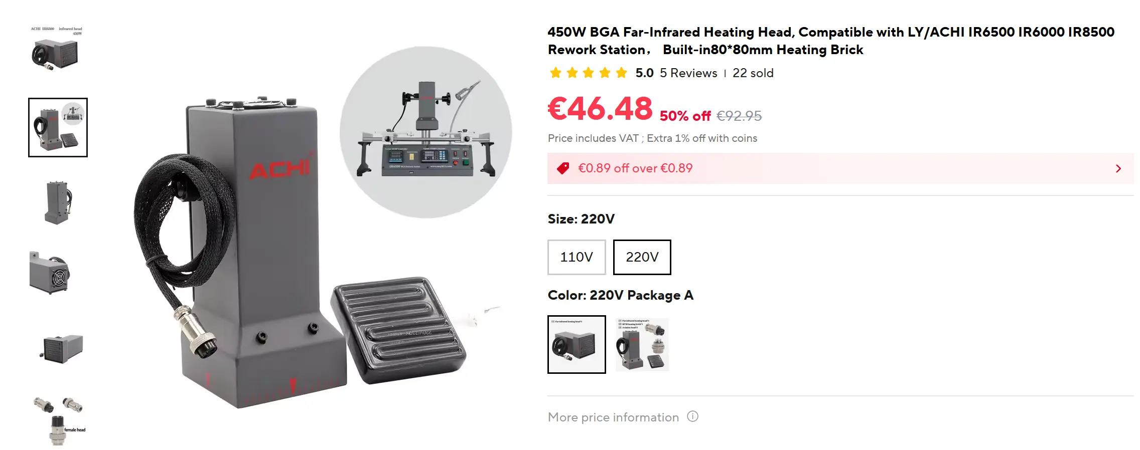
However… The IR top heater never arrived… Ali Express says it did, but it ain’t here :/
So, I guess I have to keep practicing with hot air till I get the skill down...
Along with the main PICO board, I also ordered some cheaper 2 layer boards, including a simple test dock which fits the AVE, and some regulators, and other simple features. It’s there to power the PICO and to get the graphics data out, so that I can test if the boards works when I finish soldering it.
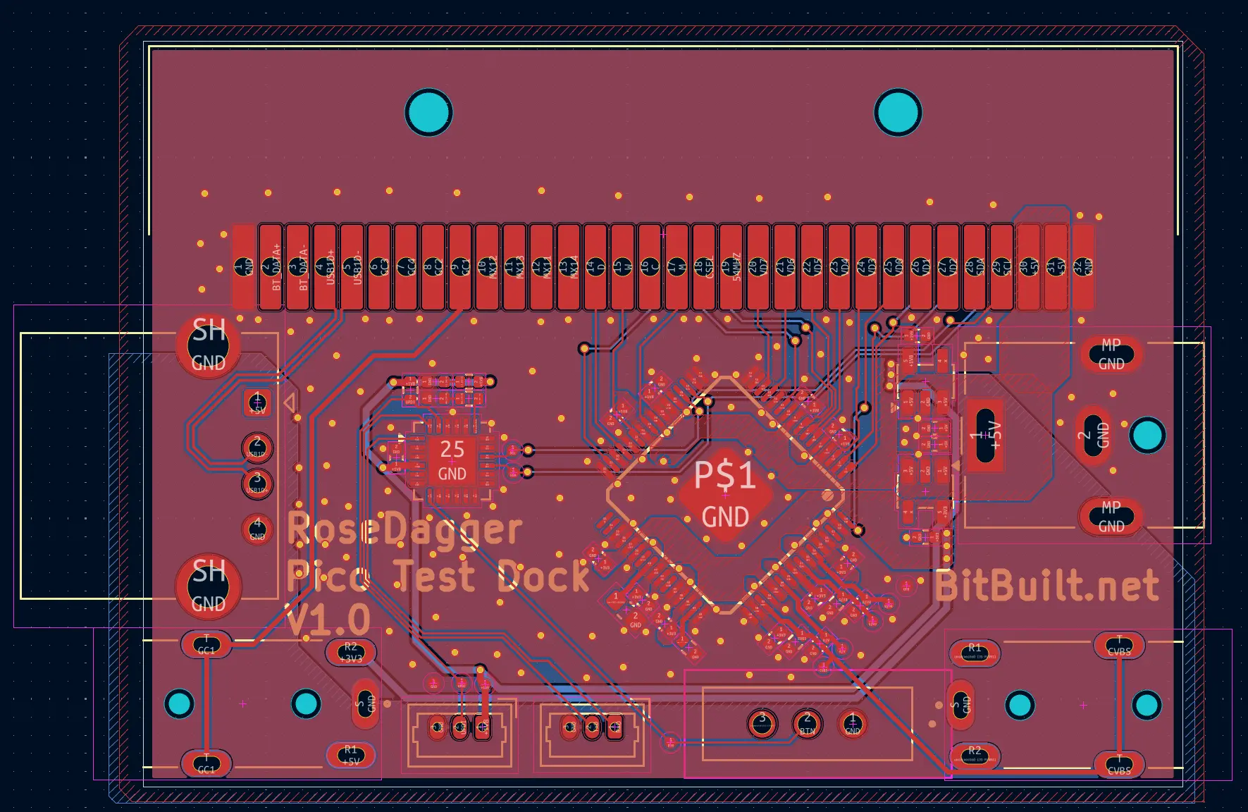
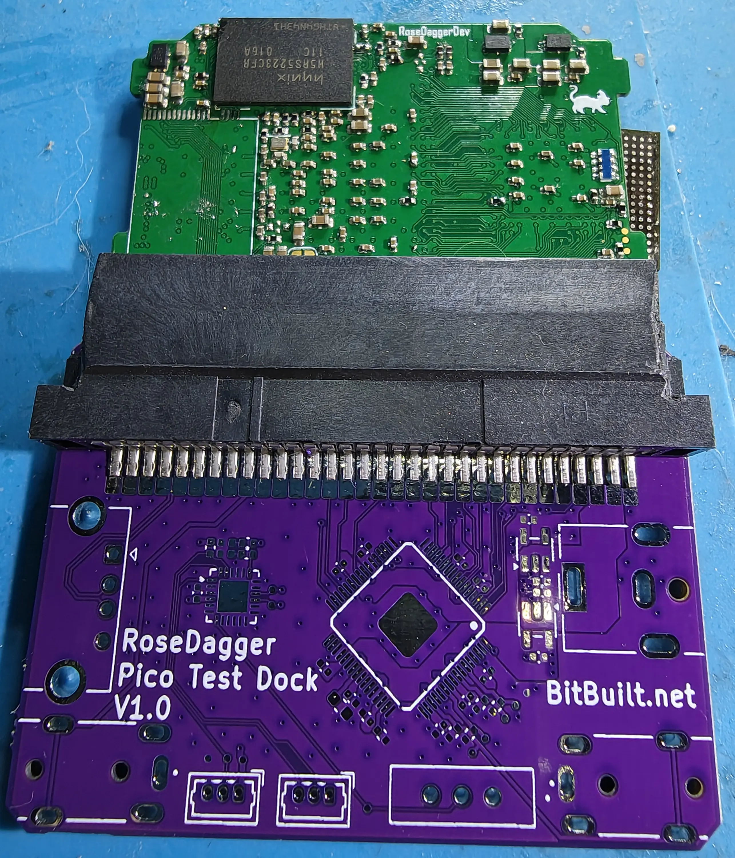
I plan to make a nicer TV dock, and the GBA handheld dock later, however I first need to test if the PICO even works to begin with.
Now while aggressively waiting for the PICO PCB to be manufactured, and now while casually waiting on the HW2 to arrive, I’ve been working on some 3D modelling, CAD’ding out the GBA as much as I could, starting with recreating all the buttons, down to the rubber domes XP Using the Wesk scans for reference, and calipers on the parts I have at home.
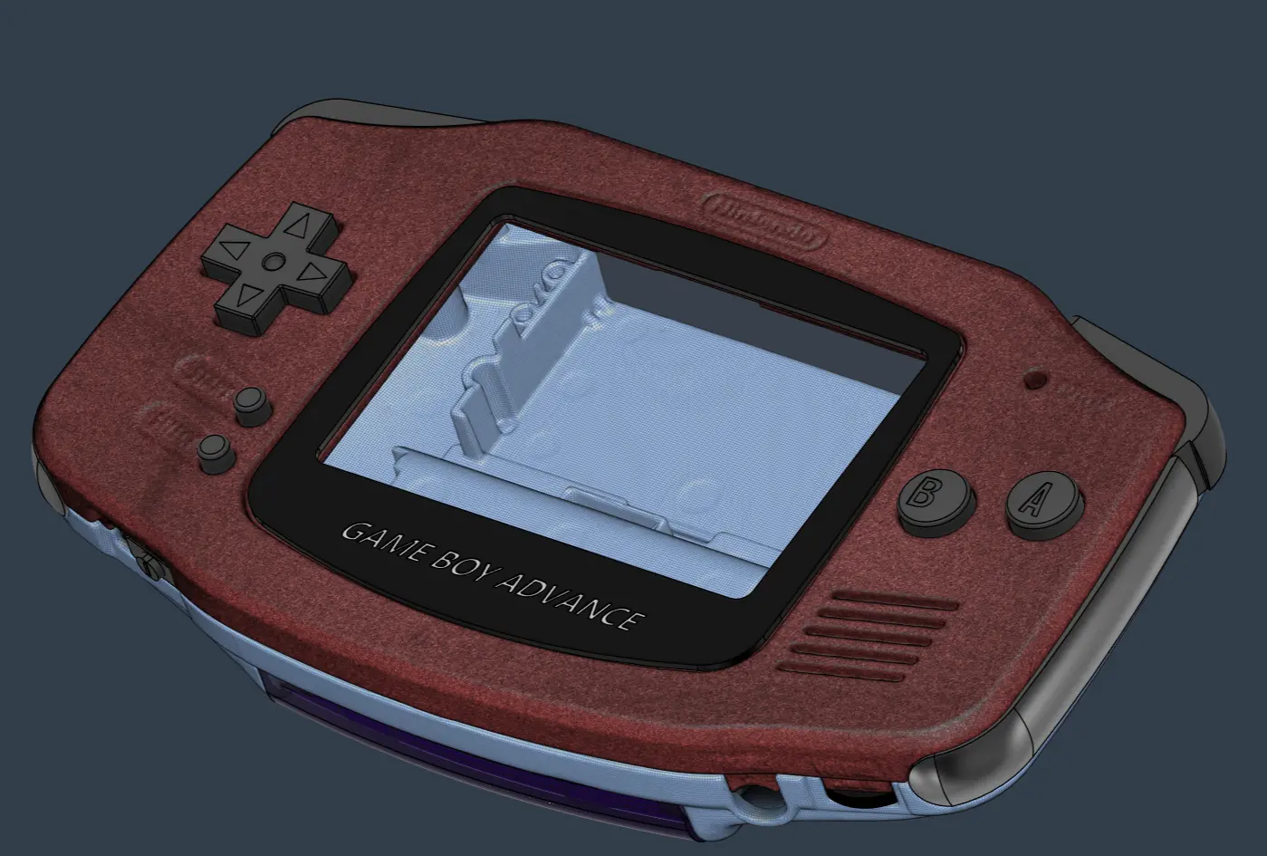
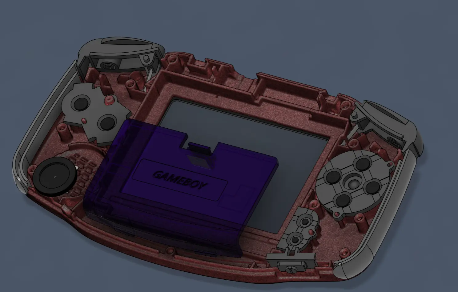
I also modelled the full shell in in fusion, trying to keep it as accurate to the stock GBA as I could. Even managing all the painful curves on the backside using lofs. (Apparently there's an option to change how the loft's connect, letting you use tangents or curvature, which helped with the smoothness)
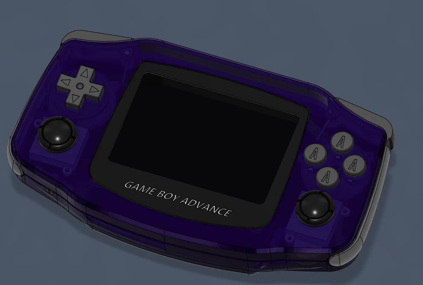
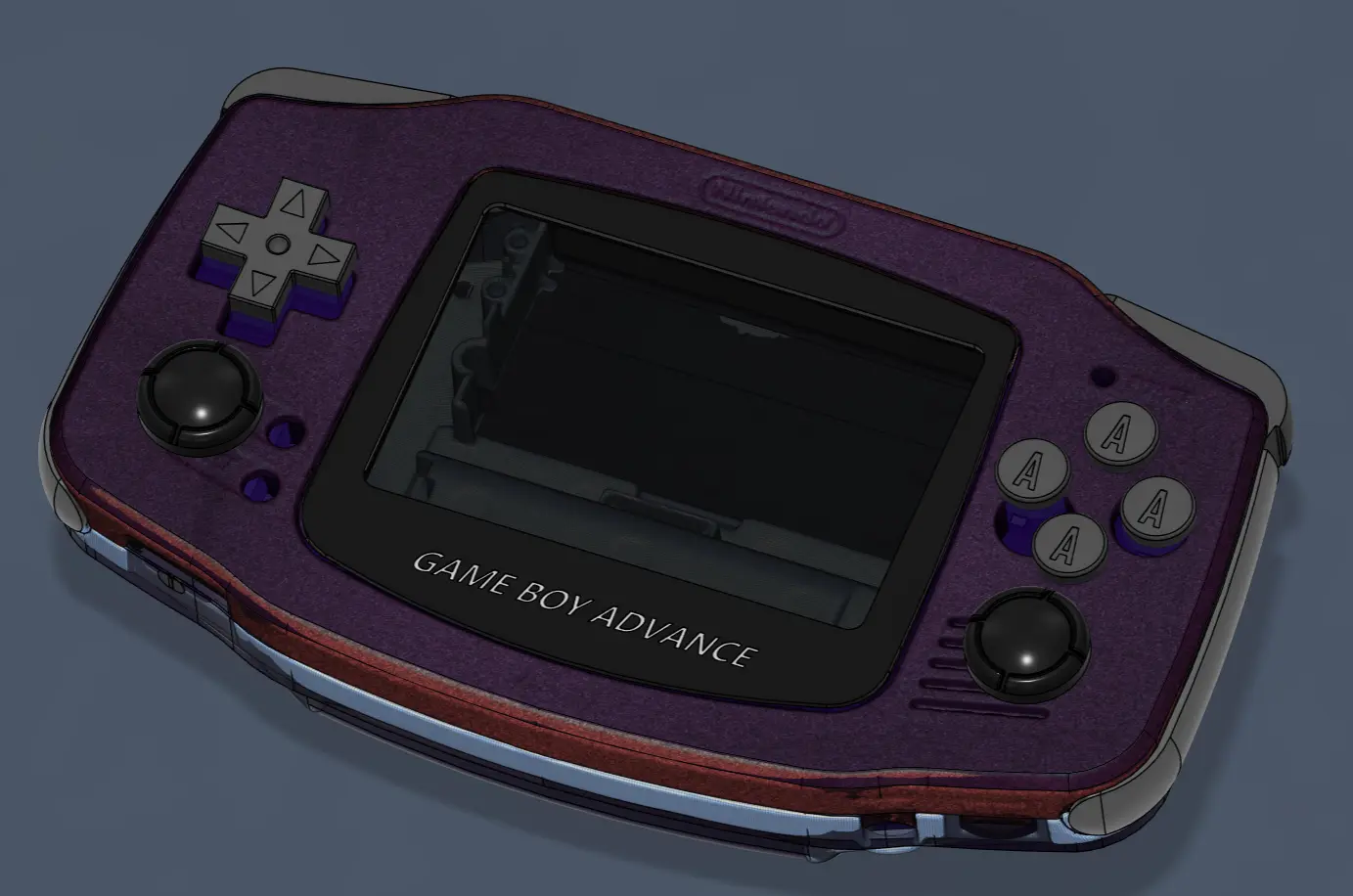
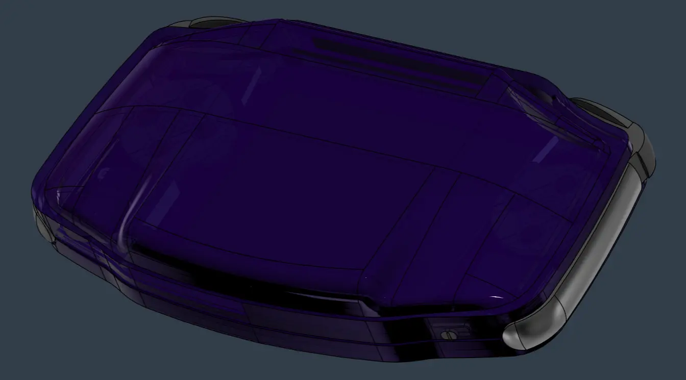
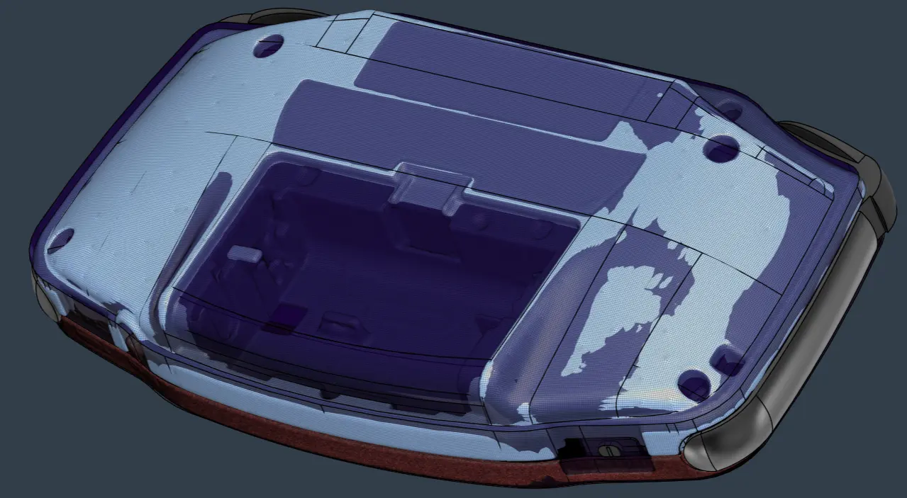
I had planned to print it today so that I could include it in the update, but half of the print came loose early on and turned everything into a mess… And I didn't realize in time to start another print today :/
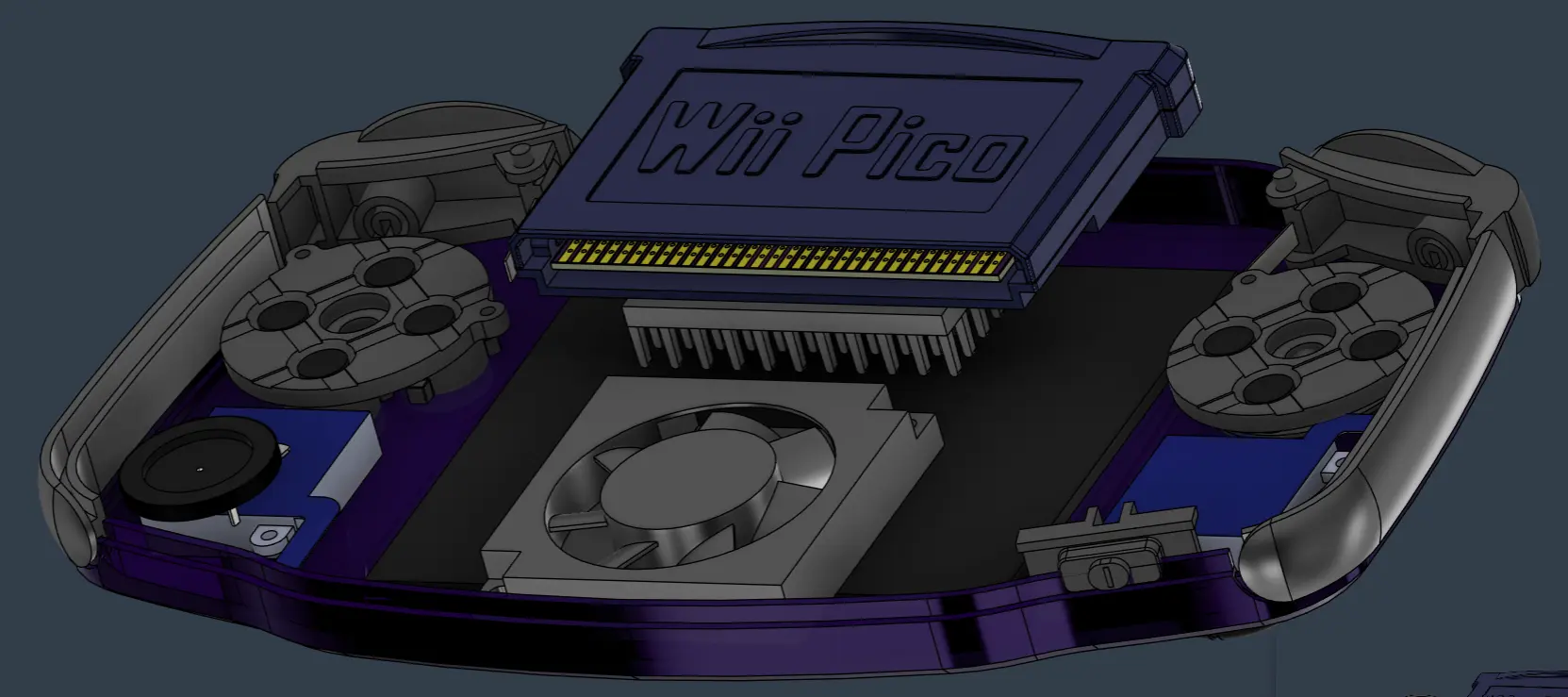
However, with 3D models in place, I also started looking at the internal layout and how to cool everything! Even though the Wii uses very little power, having no cooling while being this small feels like a bad idea XP
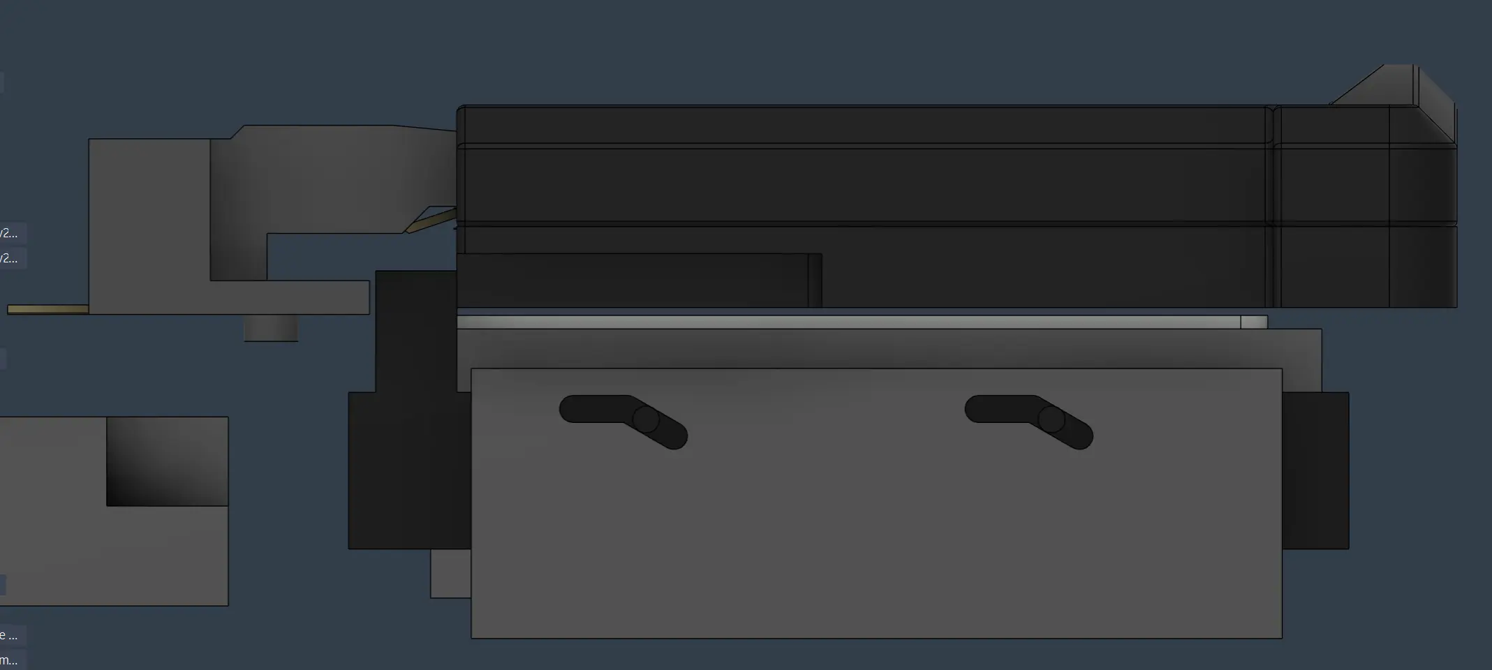
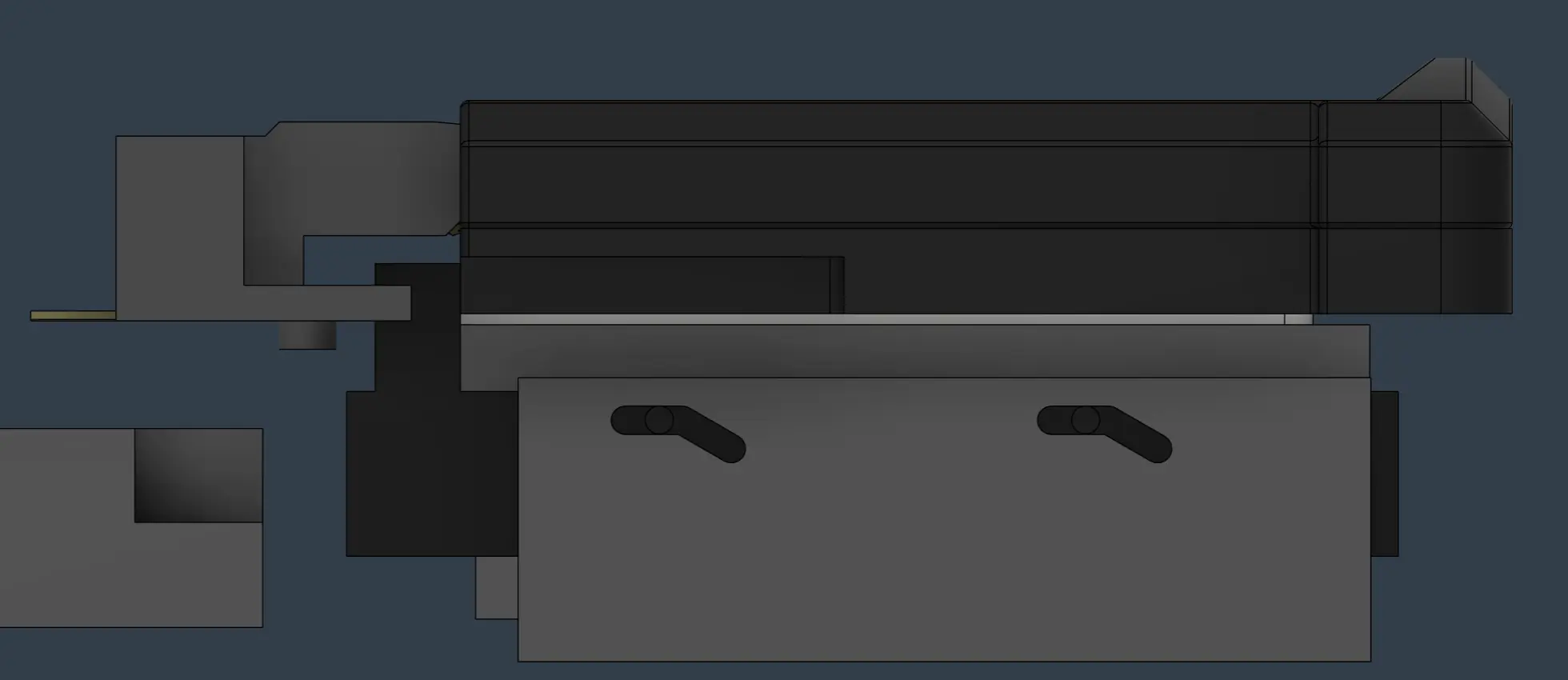
Though, with the Wii being in the cartridge, and the cart being removable, we meet the problem of how to attach a heat sink to it while it is inserted?
My current plan that I like is this:
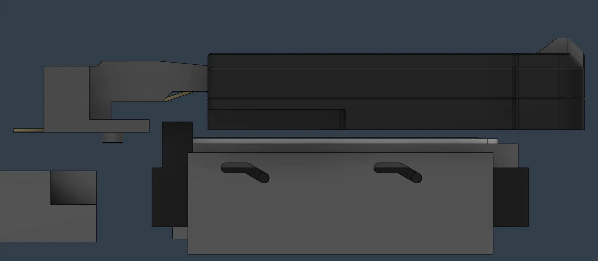
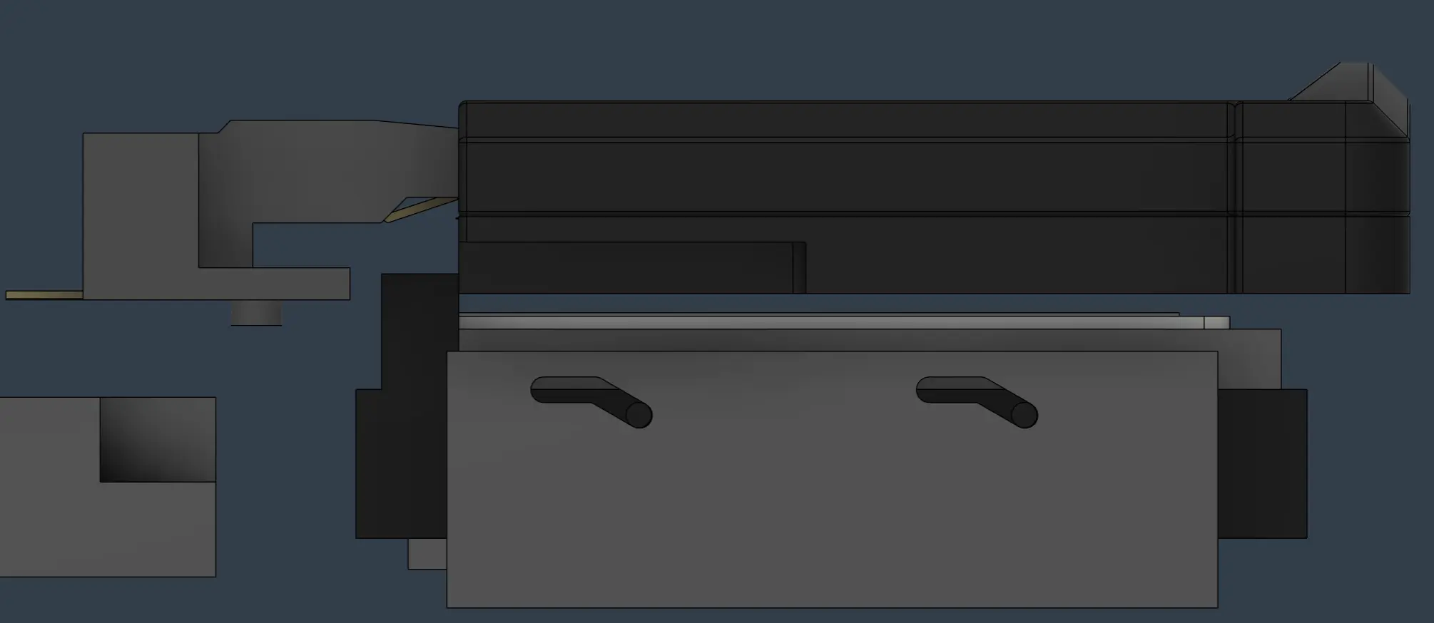
Are there better ways of doing this? Yes probably. I could get rid of the interlinked system and use an external button to do the same. I could also use springs more to give contact pressure. I could use graphite for thermal interface instead of thermal pads. But this is my plan for now, I want to make some tests based on this to see how well, or how badly this will work before I abandon it.
---
And I think I will leave it here for now XP
I need to wait on the Wii Mini with the HW2...
Practice hot air reballing more. :/
Finish up soldering the top of the PICO and solder the test dock. ^^
Then actually test if the wii will boot XP
I got the boot debug pads exposed so if there is any life in it I will be able to get something, hopefully XP
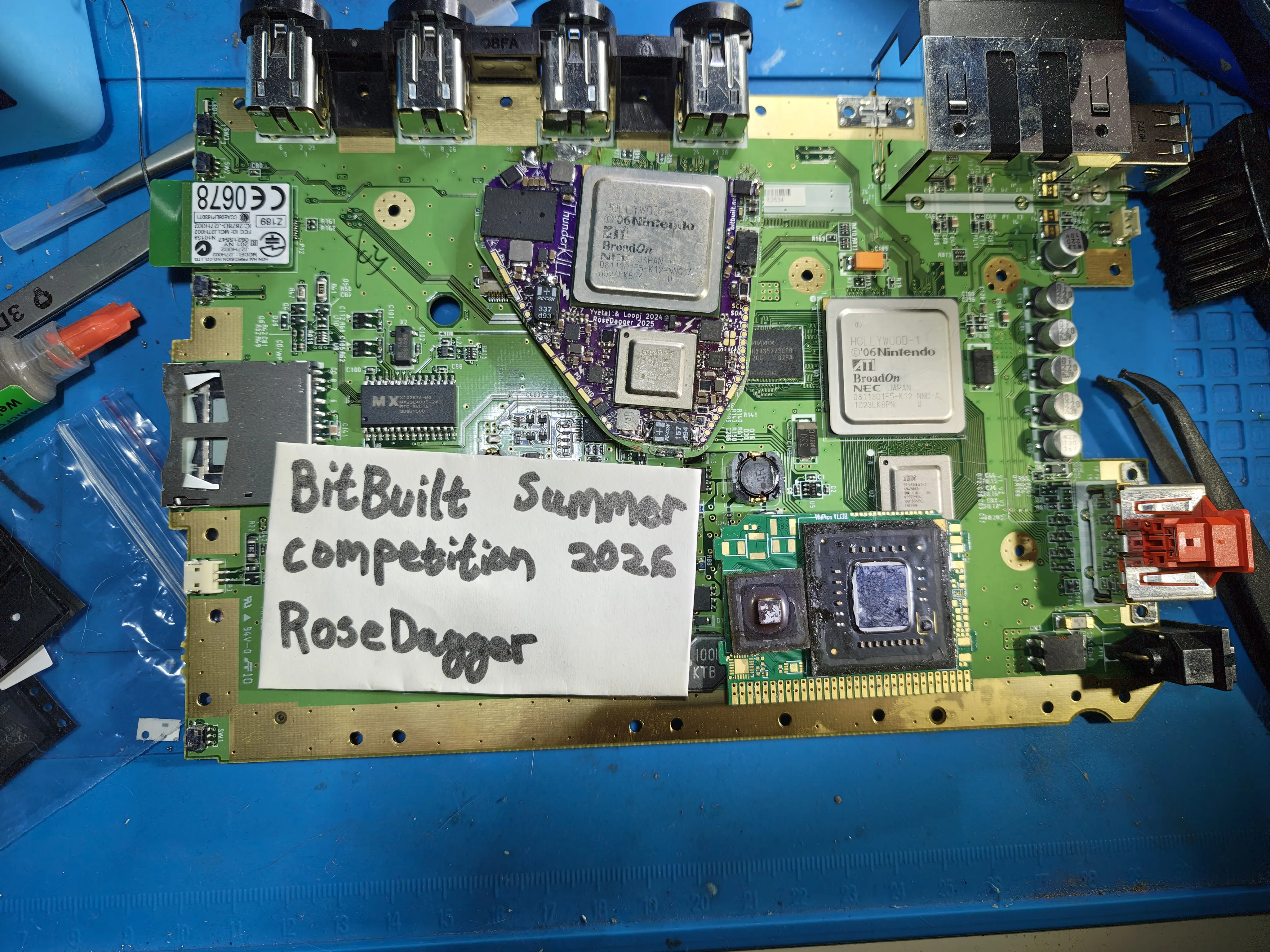
Anyway that's enough for this update. Maybe I'll have something booting in the next one, or I'll be deep into debugging and learning from potential mistakes XP
Quite a bit has happened since last time! First off after some back and forth I decided to make a version where the tracks were straight and not length matched. Primary reason being that skew would not be large enough to matter anyways, and it would let me spread some of the traces further apart to limit cross coupling.
However, being stubborn and not wanting to admit all the time I spent length matching was a waste, decided to just make a panel with both the length matched traces, and the straight traces, so that I could test both XP
I’ll include a detour into impedance matching, that turned out to be irrelevant, and can be skipped if you don’t care XP
I found the calculations for the impedance for the ram, which was set to 45 Ohm +-10%. While the PPC750 which the CPU is based on also mentions an impedance of ~45 Ohm. So, I went back to the calculator in KiCad, and double checked that with a 1oz copper weight, we would get 65 Ohm impedance on the traces, while a 2oz copper weight would drop the impedance to 55 Ohm.
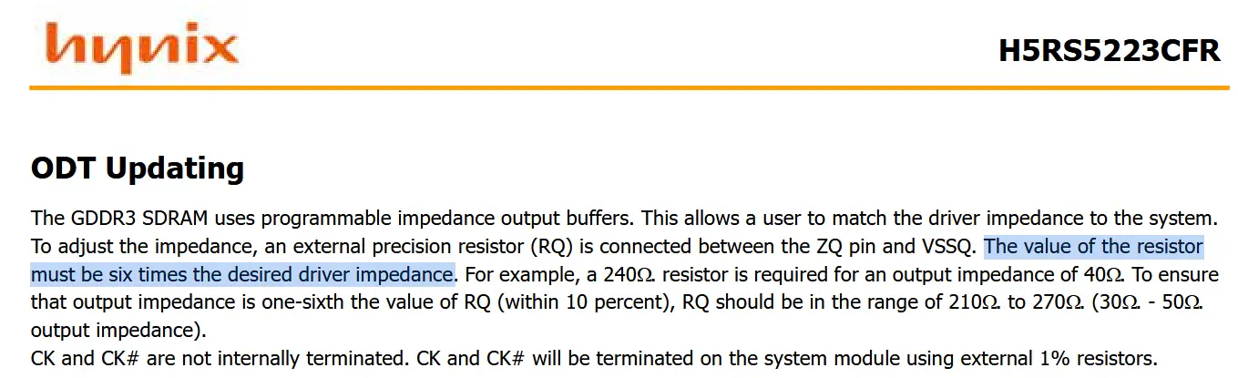
Stock ZQ on the Wii is 270 Ohm, so the impedance is 270/6=45 Ohm. ZQ should be between 210 and 270, which is an output impedance of 30-50 Ohm (using +-10% for the extremes). Changing the ZQ higher could increase the impedance, but it would go outside what the ram is built for.
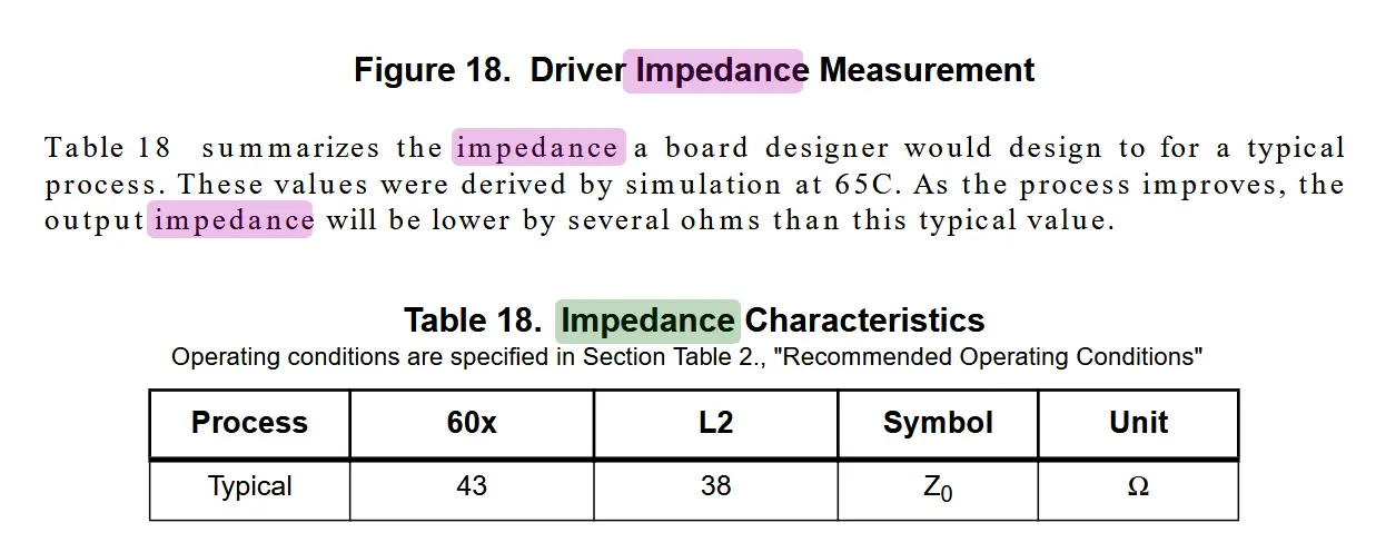
Meanwhile the Power PC 740-750 also mentions 43 Ohm without any option to change it the way the RAM ZQ can be changed.
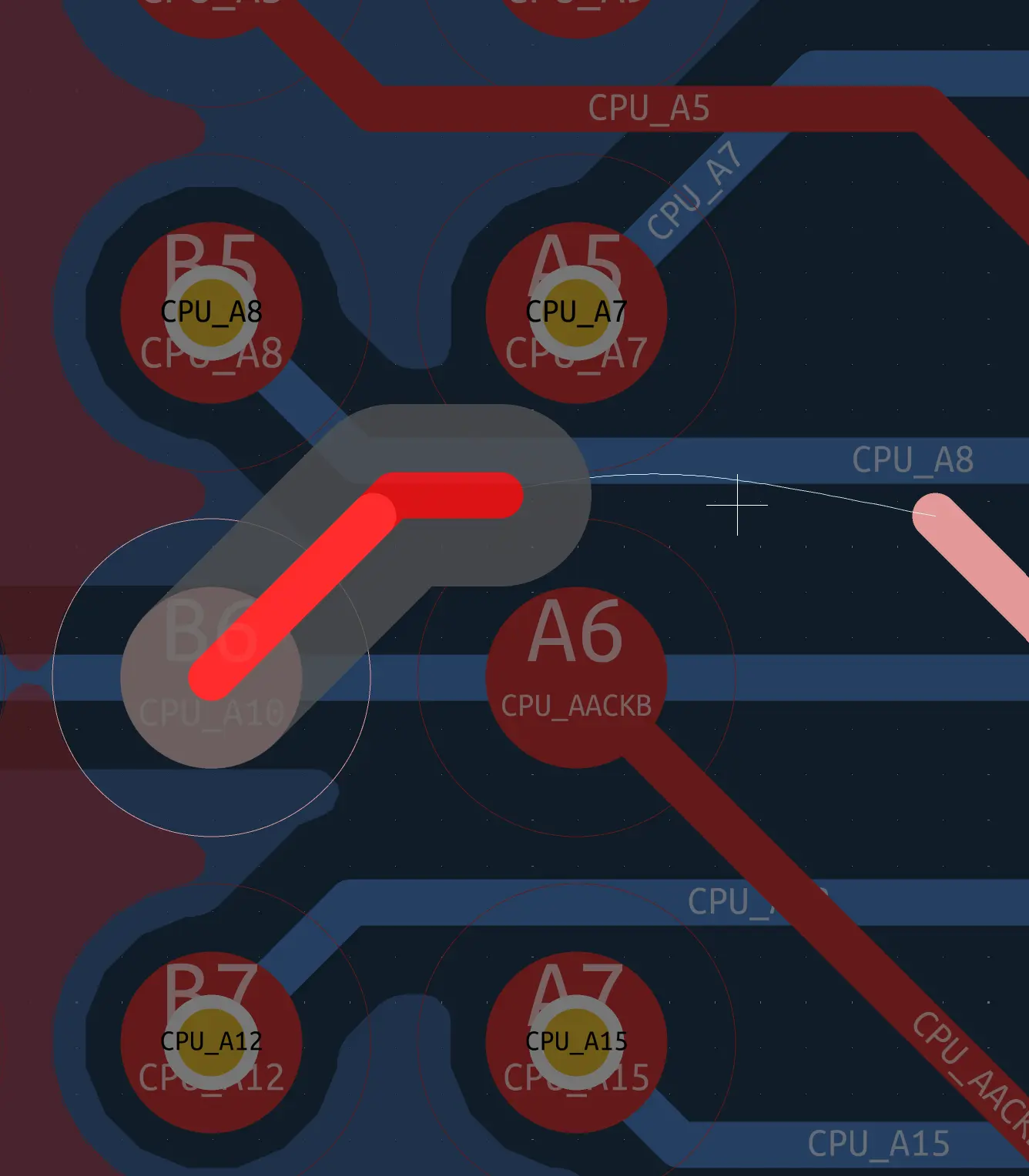
Rob’s recreation used 1oz and the same trace width, so he had it running with 65 Ohm impedance traces. However I got paranoid that since my design is so compact and deviates from the stock design so much, I though that maybe trying to go for a lower impedance might improve my chances, or at least not hurt them. Not that the lower impedance would change the cross coupling, but that if I had multiple noise factors, then removing the noise from signal reflection from bad impedance matching could improve the overall signal integrity. And it didn’t cost that much extra for the upgrade, so it seemed worth it.
However, I had forgotten a tiny little detail… Changing the copper weight changes the minimums… Instead of having a trace spacing of 0.1mm, I now needed a spacing of 0.15mm… Which would be completely impossible… That amount of spacing would mean you can’t snake traces out from the CPU pins. Maybe you can use lower minimums in BGA fanout, but I wanted to order the boards quickly, so I decided to drop it.
Stock ZQ on the Wii is 270 Ohm, so the impedance is 270/6=45 Ohm. ZQ should be between 210 and 270, which is an output impedance of 30-50 Ohm (using +-10% for the extremes). Changing the ZQ higher could increase the impedance, but it would go outside what the ram is built for.
Meanwhile the Power PC 740-750 also mentions 43 Ohm without any option to change it the way the RAM ZQ can be changed.
Rob’s recreation used 1oz and the same trace width, so he had it running with 65 Ohm impedance traces. However I got paranoid that since my design is so compact and deviates from the stock design so much, I though that maybe trying to go for a lower impedance might improve my chances, or at least not hurt them. Not that the lower impedance would change the cross coupling, but that if I had multiple noise factors, then removing the noise from signal reflection from bad impedance matching could improve the overall signal integrity. And it didn’t cost that much extra for the upgrade, so it seemed worth it.
However, I had forgotten a tiny little detail… Changing the copper weight changes the minimums… Instead of having a trace spacing of 0.1mm, I now needed a spacing of 0.15mm… Which would be completely impossible… That amount of spacing would mean you can’t snake traces out from the CPU pins. Maybe you can use lower minimums in BGA fanout, but I wanted to order the boards quickly, so I decided to drop it.
So, I felt ready to order, I had triple checked everything. Made both a length matched version and a straight version (during pride I know XP ), and made my own panel. I checked the design against the DFM tool for JLC, the uploaded the design and toggled all the important settings:
- 6 layer board
- 0.8mm board thickness
- 2oz copper
- The smallest vias JLC allows 0.15mm
- Castellated edges
- Color Purple!
And saw with dread how every option increased the price... But I decided to bite the bullet anyway!
JLC says their review should take between 10min to an hour… An hour came and went… Then two… I checked when they were supposed to be open, and they are supposedly running 24h during weekdays. So, I keep waiting, trying to busy myself with other things... It’s a complex circuit, it’s no wonder it is taking extra time… At the five and a half hours mark it finally went through, whoop! They up charged me more for the panel but otherwise seemed like I was in the clear, double whoop! So, I paid and went to sleep in the knowledge that everything would be fine.
Foreshadowing is a literary device...
Anyway... The next morning, I saw I had an email from their techs... telling me that with the 2oz copper I had ordered, I no longer met their minimums. This was apparently not caught in their initial review… I talked it out a bit on the discord before deciding to print a test print on 1oz instead and remove all the expensive options I could to bring the cost down.
So, I got rid of the panel, only ordering the straight ( :/ ) trace version, in 1oz copper, in boring green, and without castellated edges. It got the cost way down, and would make it easier to do a reprint in case I'm not a goddess of perfection XP , and there were any issues which slipped by.
Then in intensely waited for a week till the boards arrived on Thursday XP
They are kinda scary small the PICO is! And it turned out quite well even if it isn't purple ^^ Though I missed out on putting “2026 Nintendo AGB-RVL-01” on the bottom silk screen. But maybe for a second print if I needed it.
This weekend I started soldering, focusing on the back. However, I discovered that I had ordered the wrong feedthrough caps, ordering 100pF instead if 1uF. I have no clue how I picked the wrong size that badly... So got to make another order and get the right ones this time. Good thing I almost never make mistakes XP
I had planned to be stubborn and just use the regular Hollywood 1 from the regular wii I just got for this. However I was convinced on the discord to not be stupid and to just order a Mini so I can get better thermals and better undervolting. Thanks everyone ^^ And thanks to flux_sniffer for helping me on how to source the correct mini version ^^
As for the actual reballing process… Lining up the balls is fine, but getting them to melt into place without moving using hot air is kinda a pain. So I decided to cheat XP I decided to try and build an IR top heater so that I could melt the balls into place without hot air. I found a guide, the components, some aluminum extrusions to make a thing to hold it, ordered everything, and felt quite clever about myself finding a way to avoid doing something really difficult XP And I do a lot of smd soldering so it felt like an investment regardless, just putting my boards under the IR top heater to melt everything all at once as if I were baking the board.
However… The IR top heater never arrived… Ali Express says it did, but it ain’t here :/
So, I guess I have to keep practicing with hot air till I get the skill down...
Along with the main PICO board, I also ordered some cheaper 2 layer boards, including a simple test dock which fits the AVE, and some regulators, and other simple features. It’s there to power the PICO and to get the graphics data out, so that I can test if the boards works when I finish soldering it.
I plan to make a nicer TV dock, and the GBA handheld dock later, however I first need to test if the PICO even works to begin with.
Now while aggressively waiting for the PICO PCB to be manufactured, and now while casually waiting on the HW2 to arrive, I’ve been working on some 3D modelling, CAD’ding out the GBA as much as I could, starting with recreating all the buttons, down to the rubber domes XP Using the Wesk scans for reference, and calipers on the parts I have at home.
I also modelled the full shell in in fusion, trying to keep it as accurate to the stock GBA as I could. Even managing all the painful curves on the backside using lofs. (Apparently there's an option to change how the loft's connect, letting you use tangents or curvature, which helped with the smoothness)
I had planned to print it today so that I could include it in the update, but half of the print came loose early on and turned everything into a mess… And I didn't realize in time to start another print today :/
However, with 3D models in place, I also started looking at the internal layout and how to cool everything! Even though the Wii uses very little power, having no cooling while being this small feels like a bad idea XP
Though, with the Wii being in the cartridge, and the cart being removable, we meet the problem of how to attach a heat sink to it while it is inserted?
My current plan that I like is this:
- Put the heat sink on a cammed track.
- While the cart is not inserted the heat sink will be in the down position, held in place by a spring.
- As the cart is pushed in, it will push against an arm on the heat sink, pushing the heat sink forwards with the cartridge.
- As the heat sink moves forward, the cammed track pushes the heat sink upward into the cartridge, with a bit of force to allow for good contact.
- A thermal pad on the heat sink, will act as the thermal interface material, and a soft buffer.
Are there better ways of doing this? Yes probably. I could get rid of the interlinked system and use an external button to do the same. I could also use springs more to give contact pressure. I could use graphite for thermal interface instead of thermal pads. But this is my plan for now, I want to make some tests based on this to see how well, or how badly this will work before I abandon it.
---
And I think I will leave it here for now XP
I need to wait on the Wii Mini with the HW2...
Practice hot air reballing more. :/
Finish up soldering the top of the PICO and solder the test dock. ^^
Then actually test if the wii will boot XP
I got the boot debug pads exposed so if there is any life in it I will be able to get something, hopefully XP
Anyway that's enough for this update. Maybe I'll have something booting in the next one, or I'll be deep into debugging and learning from potential mistakes XP
Attachments
Last edited:
- Joined
- Jan 15, 2021
- Messages
- 68
- Likes
- 267
- Portables
- Wii PICO (Complete), Wii Zero (WIP), GBAWii4 (WIP), GB Adwiince v3 Revenge (On Hold), GB Adwiince v2 (Dead)
1. Preamble jabber
Heya, so maybe it’s time for another update, it’s only been, let me check… a month and a half since the last one XP
So very little and a lot have happened in that span, but to pick up where we left off last time where I said
I’m definitely in the latter of those two options, and if you are interested mostly in how that’s going, you can skip to the debugging section. Otherwise let me take you through the meandering path of trying to get good chips to harvest.
Note from later me, this entry turned very, very, very long, I’ve split it into sections:
2. The quest for HW2
2.1 The adventures of Chipped Charlie
So last time I had just gotten the PICO boards, and started soldering it up, and had a regular Wii with a HollyWood 1 that I had planned to use. But I got convinced into ordering a Wii mini so I could get a HW2 which uses less power and has better power efficiency. For a tight build like mine it made sense, though it would delay be a tiny bit having to wait 2 weeks for the Wii mini to arrive. Looking back with hindsight I should have used the HW1 I had as an experiment to see if the PICO worked, then worried about the HW2 later… But it was only a 2 week wait, so I could work on the 3d model for the GBA case, no biggi.
So, the first Wii mini arrives, however, before anything else, I’m going to give it a name, I already have a few Wii’s laying around, and spoiler, I’ll get a few more. Names will help separate them.
So, I check that Charlie boots, install RVLoader like I’ve done on a half dozen Wii’s before. Then bake Charlie. Unfortunately, I don’t have a PCB oven, so I decided to use my preheater. I put Charlie upside down on the preheater, so that the CPU and GPU gets baked, and let him sit for 6h. I was recommended 100C for baking, and using some temperature probes, I saw that there was about a 20C difference between what the preheater was set to, and the board temperature, so I set the preheater to 120C, so that the board was 100C.
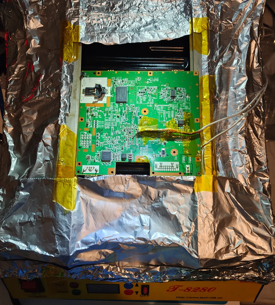
After those 6 hours, I flipped Charlie around and baked him for another 6 hours the right way up. I really didn’t want to take any chances after the last board, Alpha, turned out very very very very very dead.
Once Charlie was sufficiently baked on both sides, a full 12-hour process… I started bringing him up to temperature. Last time, with Alpha, I did it right after being sick, and had a massive headache, and rushed without thinking and without checking what was reasonable, even though I had harvested chips from PS3’s a few times before then. So, my dumb brain had done the dumb thing of: “Well I set my soldering iron and hot air to 320-350C so that’s the temperature I should reach…” Solder starts melting at around 220C… The reason the iron and hot air is set higher it to overcome the heat loss from radiating heat elsewhere, and to overcome the losses from needing to heat up the ground plane and pcb acting as a heatsink… I reached a bottom temperature of 290C… which is slightly above the solder melting point of 220C… Delaminating Alpha, making it go all discolored, delaminating the GPU, and components on the bottom side had just fallen off due to gravity… So that was slightly sub optimal…
This time, with Charlie, I checked… A reasonable bottom temperature is 180C, then you bring it the rest of the way up with hot air and start checking if the chip is floating once the top probe reads 220C. The technique I ended up using was holding the hot air nozzle very close to the GPU, counting to 30, then gently poking the GPU with a tweezer that I gently held in the far end. If the tweezer bent, then it was not ready, if the GPU moved, then it was floating, however I let it heat up for another 30 count, to be sure it was fully floating and that I was not ripping any pads, and that it would not solidify as I removed the heat to lift it up. And that seemed to work well, I got the GPU and CPU and RAM off without issue, there was no popcorning on Charlie, and checking the resistances one the GPU and CPU they turned out fine. (I’ll post about the resistances in a later segment.)
However, I was not yet quite done, so after spending 12 hours baking Charlie, then more time carefully heating him up to temp slowly and harvesting the chips, I decided to do the next step right then and there before going to sleep. Because the best work you do is while tired before going to sleep… So, what did I need to do? Well since I needed every fraction of a millimetre of space for the PICO, I needed to delid the GPU and CPU, so their height would be slightly smaller… So, I did as last time, I took a razer blade and carefully cut the glue around the edges of the IHS, making sure to angle the blade slightly upwards so it would not scratch the substrate. I did the corners first, careful about not going too far in. Then I did the edges. Then after working it for a bit, the IHS popped off, and I could see the silicon die, and the caps around it, and the tiny silicon die which others in the discord identified as the EEPROM. Everything looked great! There were no popcorning visible, no scratches, no defects I could see. So, I posted it in the discord, and we looked at some of the differences between the HW1 and HW2, along with the empty slots for caps. Then just as I was about to sign off, Rob noticed something, a potential defect, just from the image below. Can you spot it before I point it out?
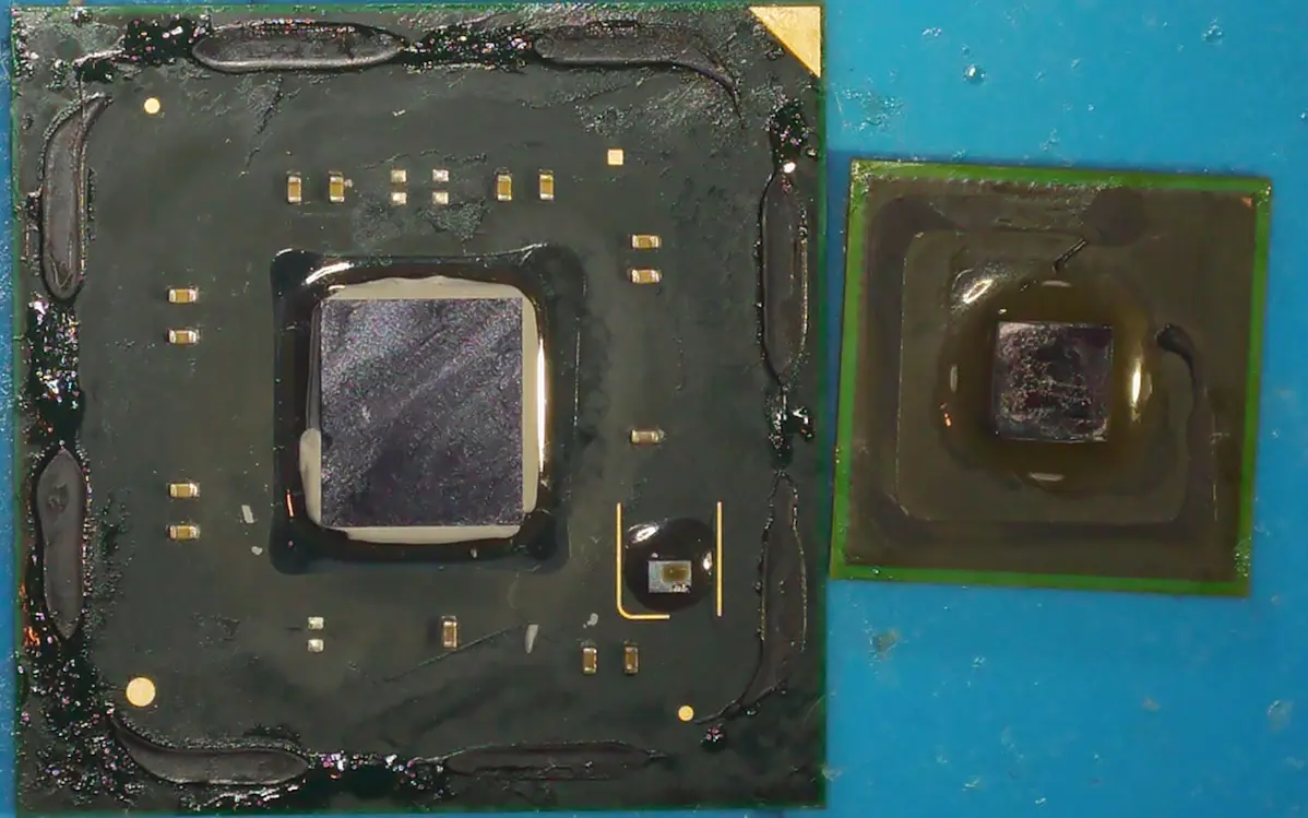
So, the HW2 from Charlie was potentially dead, and the only way I could check was to test it… But I had just removed the GPU, CPU, RAM, and NAND from Charlie, and I really didn’t want to put them back on. Though from the discord I got the suggestion to put the GPU onto the working regular Wii I had, aka Bravo, though as the NAND and GPU are married to each other, and I didn’t dump the keys, I needed to transplant both. Though as it was Sunday, and I had work the next day, and baking takes a long time, I needed to wait till the next weekend. There was also a risk in transplanting the GPU, as according to Rob, the vias on the stock Wii makes it difficult to transplant a GPU back onto a stock Wii without creating bridges… You need it to sit perfectly and not shift… So, it was mostly a hail Mary (good movie and better book btw) to see if the HW2 from Charlie was still good. So, I ordered a second Wii mini (Delta), just in case the HW2 I had from Charlie was dead.
2.2 Brave Bravo
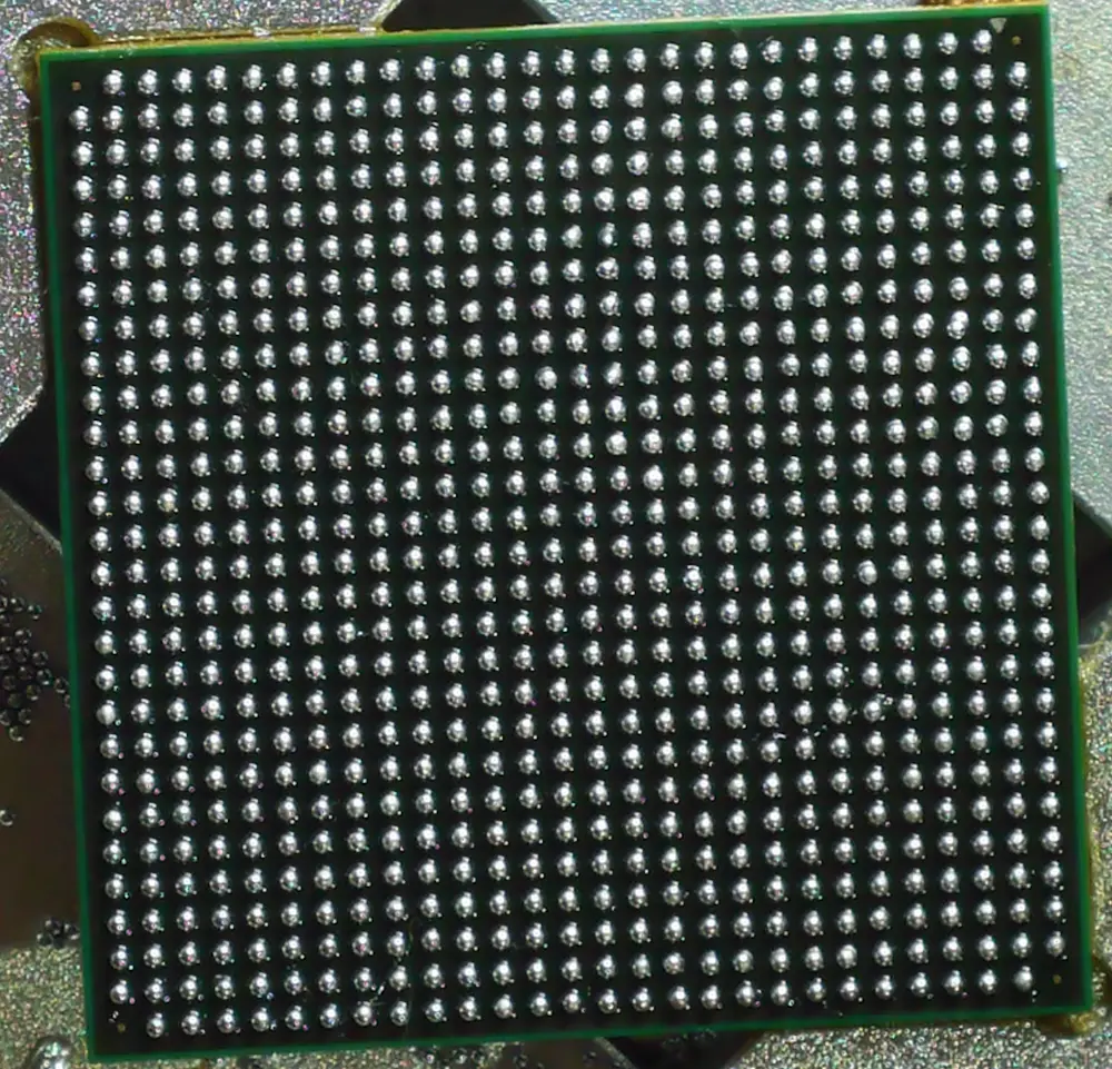
During the week I had, I spent my afternoons practicing reballing on the very dead GPU from my first attempt aka Alpha, and I got better and better at it. The first proper attempt. I had about 10 solder bridges (error image not found). My second attempt I had 1 solder bridge, which merged into a big ball, I tried to rescue it with solder wick but just made a bigger mess. My third attempt I had issues with the balls not wicking down, so after I was done, I found several balls who were not seated, so I heated it up again… and managed to bump into a bunch of the balls with the hot air nozzle… The fourth attempt I used more flux so the balls would wick better. I had to stop a few times as the balls started floating together, and I needed to separate them before they formed a blob, but I got a perfect reball!
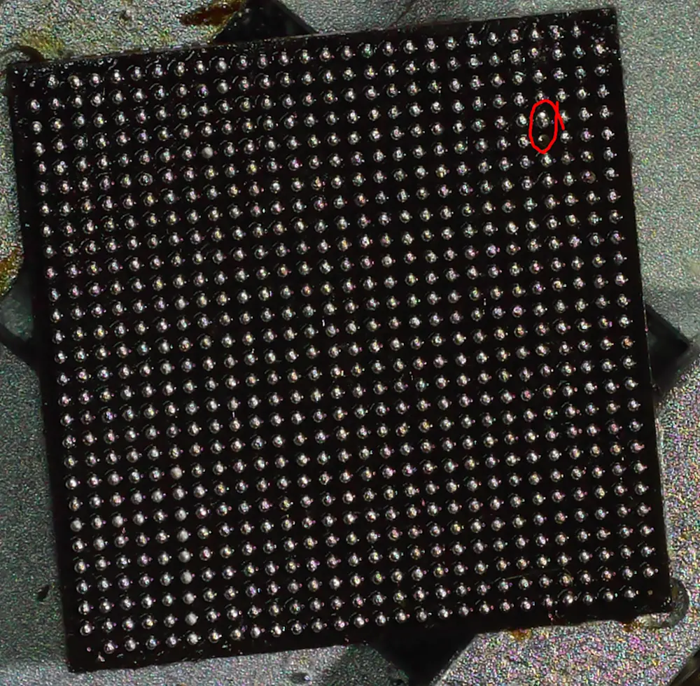
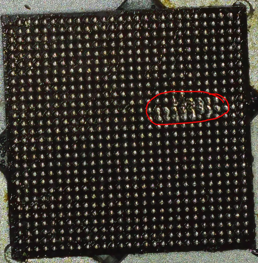
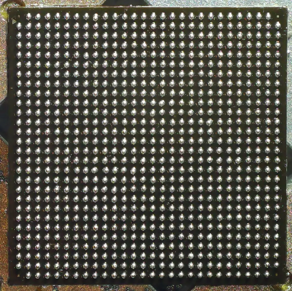
Then I did the exact same thing to the to the chipped HW2 from Charlie and got it on my first try!
Then next weekend come around, and I start going through the procedure again with Bravo. Last time I did 6 hours on each side, however as the temperature probes on the top and bottom were relatively close, I decided to do 3 hours upside down, then 6 hours right side up, so it was only 9 hours of waiting on Bravo. Then I bought Bravo up to temp, and started blasting the GPU with hot air, this time being even more careful to not rip pads. It had gone well last time, but I really really needed it to go well this time. I poked it gently till it was floating, then waited a bit longer, then lifted it. No ripped pads! I cleaned it up, using leaded solder then solder braid, before I put down fresh flux and placed the Charlie HW2 down onto Bravo. Then I started blasting it with hot air, waiting till the probe reached 220C, and repeated the same procedure to check if the balls had melted and that it would bouncing back into place. I removed the hot air, and let Bravo cool down, and turned off the preheater. Then flipping the board while it was still hot, I removed the Bravo NAND and placed down the Charlie NAND.
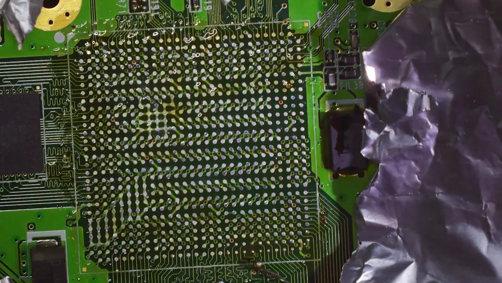
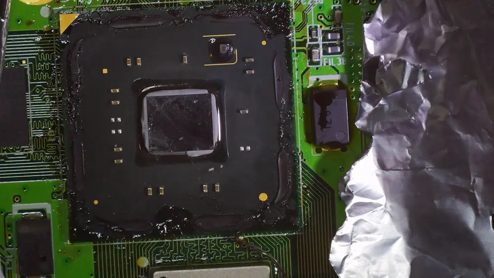
I needed to clean up the legs of the Charlie NAND, but then it was time to see if it would boot. I checked the resistance which seemed fine, no shorts. I plugged in the power, and the power LED turned on. I pressed the power button, and the LED switched color. All great news! So, I kept looking at my monitor to see if I would get an image… No image… I checked the boot debug pins, and I got a flashing 0xF1… Which is EEC or RAM issue… That is step 1 of the boot process… The EEPROM is step 7… Maybe there were some bridges on the RAM side of the GPU… Maybe I had accidentally bumped the RAM chip while transplanting the GPU… I remembered what Rob said about transplants on the Wii was difficult and that it was a long shot unless I got the alignment perfect, and my method to check if the chip was ready was by poking it… My work bench is not big enough that I can have the preheater and the reballing jig out at the same time, so I would need to spend a few hours heating the board up and harvesting the GPU again, then let it cool down before I move the preheater away and try to reball the GPU again, which could take a few more hours, then I would need to move the preheater back and heat it up again, to try and transplant the GPU back… That would take ages… And I had a new Wii coming for the next weekend. So, I cut my losses and put Bravo with the Charlie HW2 aside, I could come back to them late and try again if needed.
2.3 Disappoint of Delta
The next weekend comes around, it’s now 4 weeks since the last update, I got the new Wii mini, Delta, it’s a HW2, I jailbreak Delta with bluebomb, using linux, though it’s very annoying pressing the BT reset button over and over and over and over till it connects. Then once Delta is jail broken and the homebrew channel is installed, I just need to install the RVLoader like I’ve done plenty of times before, with the plan to dump the NAND afterwards. I check the settings and change the WiFi to be patched out, and no VGA patch, and I let it install. It starts the process and everything seems fine, until it freezes at “Exitting…” which I’ve not seen before. Though it looked like it was done, so after waiting a while, I decide to just power cycle Delta, if the update didn’t take, then I could just install it again… I try to boot it… And I get nothing… The power led changes color, but I get no video out… The debug port is outputting a solid 0101 0101 which isn’t a valid code, and it’s supposed to flash (50% duty cycle signal) … I managed to brick Delta… I check the forums and the discord, and there’s been a few people who has encountered the “Exitting…” freeze, but they either didn’t manage to fix it, or fixed it without telling anyone how…
I thought back to how I changed the WiFi settings… Wasn’t the default that it was patched out… Did I patch WiFi in? The Wii mini does not have a WiFi card, the connector is not even added to the board, and the series resistors are also gone…
But I have a WiFi card from a regular Wii, so let me follow the guide and install it on Delta on the pads to the GPU just to see if it would work. So, I fiddled with magnet wire for a bit, before I got it soldered up, and I checked… Still no video out…
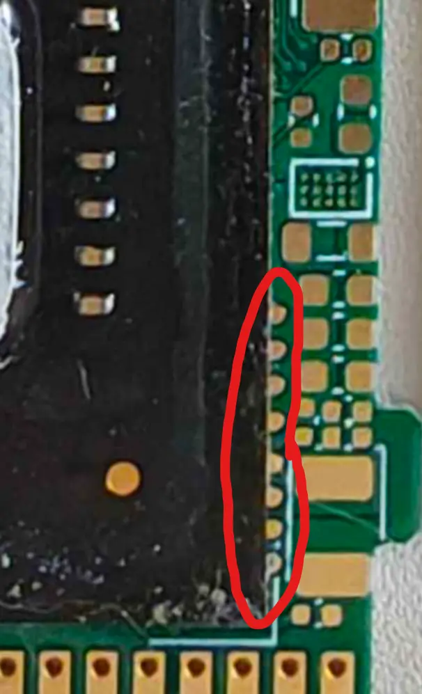
I check if there were any suggestions to others with this bug and see that the suggestion is to use the reset button to try and enter a sort of recovery or factory reset. But the Wii mini does not have a reset button… I check my spreadsheet for the reset button pin on the GPU, and check it on the Wii mini… The vias around that area is slightly different from the stock Wii, so I check the board scans for the Wii mini, and find the via, solder a button to it, and try anything I can think of… But nope, Delta is still bricked… For future reference the circled test pad is for the reset button.
Had I dumped the Delta NAND then I could have recovered, I could have written the original NAND image back, but since I had wanted to dump the NAND after installing RVLoader… And it bricked during the installation… I could not do that… So, I have a potentially broken HW2 GPU from Charlie, but working NAND, and a working HW2 from Delta with a broken NAND firmware, but since the GPU and NAND are keyed to each other, and I didn’t have those keys I could do nothing…
I ask in the discord, but no one has any suggestions beyond what I’ve already tried. So, I decide to give up on the second Wii mini. Maybe my WiFi solder job had been bad? And if I tried again, I would get it working? But I was tired and was still not sure if it was the WiFi as the other people with the “Exitting…” bug had been regular Wiis, so they should have had the WiFi card installed when they installed RVLoader. I decided to give up on Delta and just order another Wii mini (Echo), which was supposed to arrive the coming Friday, so it was only a week wait… Then thinking about my bad luck and how much time I had spent on just trying to harvest chips, I ordered another Wii mini (Foxtrot) which was supposed to arrive on Thursday.
2.4 Echo and Foxtrot, an encouraging chance to fix this mess

Well, Ebay lied, so they didn’t arrive till Tuesday the week after, and as I work over the summer, and don’t want to run the preheater while I’m away, I needed to wait till the weekend… So that was another 2 weeks wait… 6 weeks on waiting so far… I feel I’ve been here before with delay after delay…
The two Wii mini’s arrive Echo and Foxtrot, I jail break them, though bluebombing the second one took ages… Like over an hour… Think it only worked after restarting my PC to try over… So, if you are doing multiple consoles in a row, maybe try restarting your PC between each console to clear any issues? Or it was just my bad luck…
I dump the NAND this time from both Echo and Foxtrot. Then installed RVLoader, the default setting is that WiFi is patched out… I definitely patched WiFi in on Delta, a Wii mini which does not have WiFi… Anyway, the installation process goes well on both. So, I have two working Wii mini’s which are ready to be harvested. I pick one, Echo, as my third attempt, and wait till the weekend again… Though with luck on my side, I had booked a 2-week vacation to work on the PICO for the two weeks starting with that weekend, so it was just about perfect, I would have plenty of time to work on this, and to catch any bugs… Surely bug catching will be easy and no hassle…
Anyway, the weekend comes, and my vacation starts, and I echo the same steps as last time for Echo. I think I did 2 hours upside down, then 6 hours right side up, so 8 hours of baking. I harvest the GPU and CPU without issue from Echo. Delid them, without chipping the die, and check the resistances. See third time is the charm, I knew luck was on my side for once.
Note 1: For the CPU you have to measure the resistance in the middle, as the voltages around the core, and the outer ring around the core has a different resistance, some going to analog pins, some to GPIO pins.
Note 2: Some voltage rails change resistance between probes, latching high or latching low. So, I’ve listed both states.
3. The big quest for a tiny PICO
Before heading into the PICO, let’s have a look at the consoles used so far:
3.1 Why the fuck did reballing get more difficult again?
So I have the HW2 from Echo, along with it’s CPU and NAND. I had ordered some fresh RAM from Aliexpress, so that I would not need to reball the RAM myself. So, all I needed to do was to reball the GPU and CPU, and place down the NAND, easy peasy right? I’ve already gotten a technique down for reballing the GPU and didn’t have much issues with it once I got it down. Sure, that was 3 weeks ago, and I’ve not tried again since, but surely, it’s not that hard, right?...
On my first few attempts on the Alpha GPU, I had not used enough flux, and it led to the balls not wicking down, and I burnt the GPU even more trying to get the balls to melt. As I preferred to not burn up my good Echo GPU, I decided to use more flux just to be sure. However… More flux means that the balls float more and want to clump together… So, I spent the next few hours heating the chip up, carefully watching for when the balls started clumping together, then immediately stopping, and separating them. Over time the flux would evaporate, and the balls would clump less and less, until I could finally reach the temperature needed to melt them and have them wick into place. I did it zone by zone and realized that the areas where the GPU was clamped into the jig was struggling to heat up, so I took the GPU out and rotated it so that I could heat those two corners.
Nicely placed down solder balls
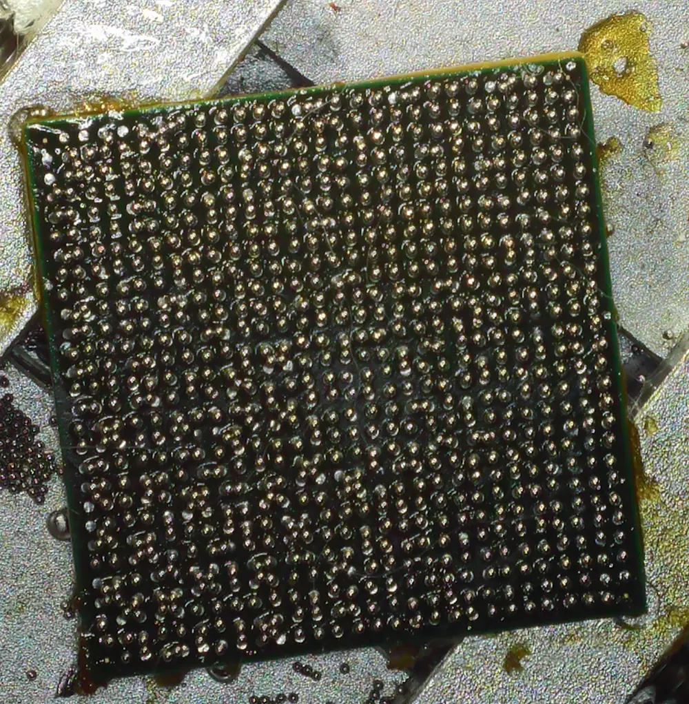
Literal hell, each ball cluster must be separated manually. Why do I do this?
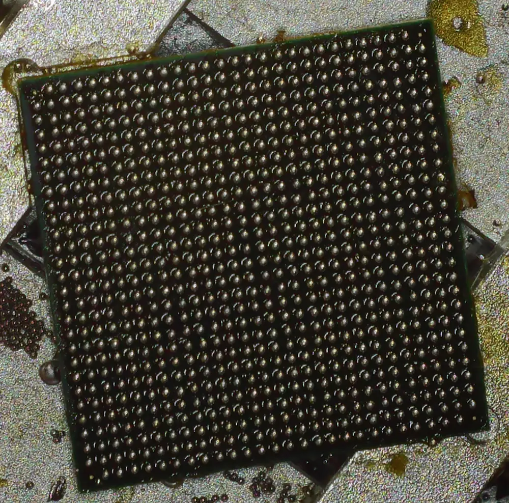
An eternity later, and it's a perfect reball...
Then over to the CPU… So, I had twice tried to get the stencil for the Wii CPU, however, even though both listings I tried said they had the Wii CPU in them, neither did… So, I ordered some generic stencils and found that the 0.4mm stencil fit, all I needed was to mask off all the excess holes. And as there’s no complex patterns on the CPU itself of where the balls should go, that turned out quite well.
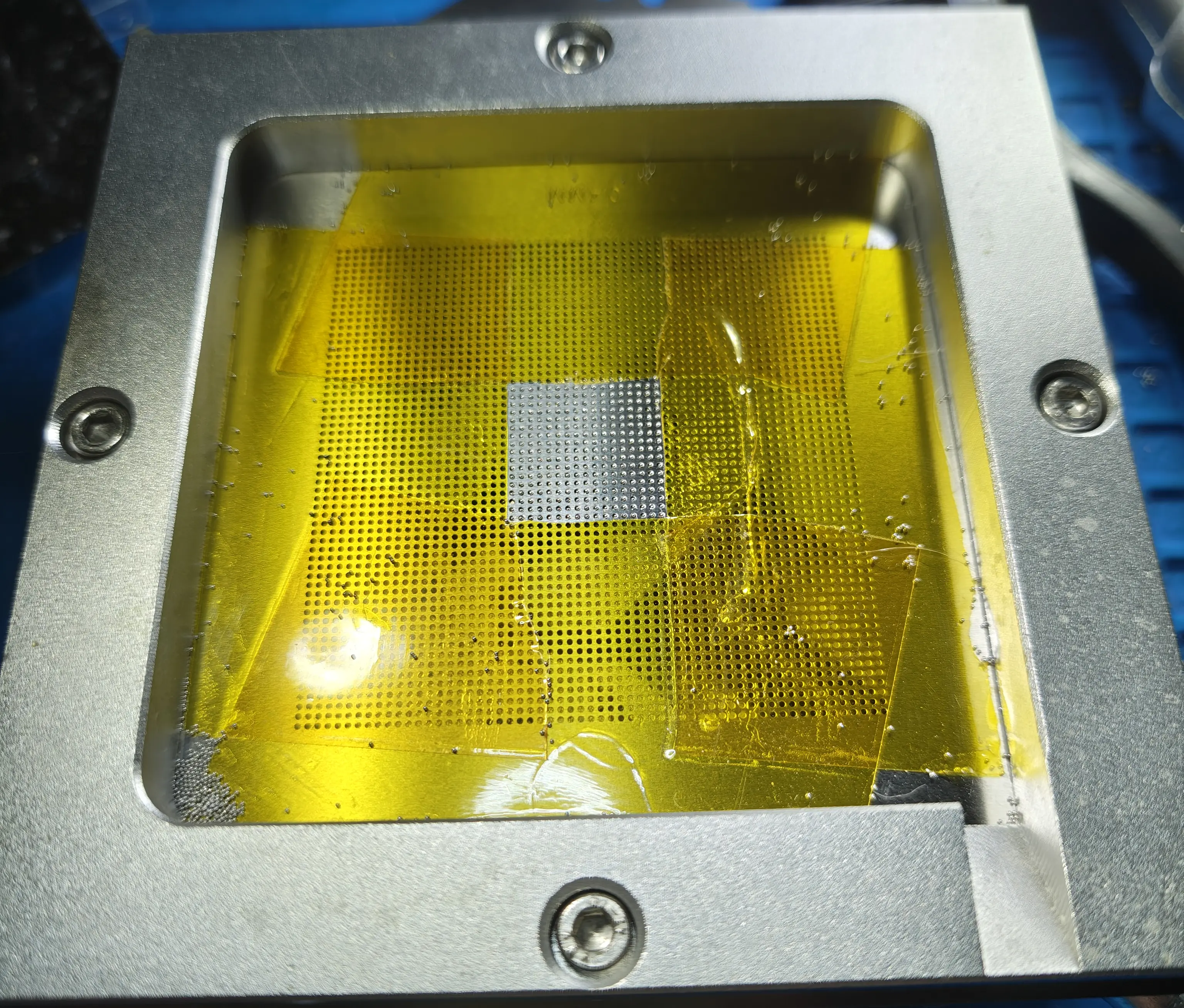
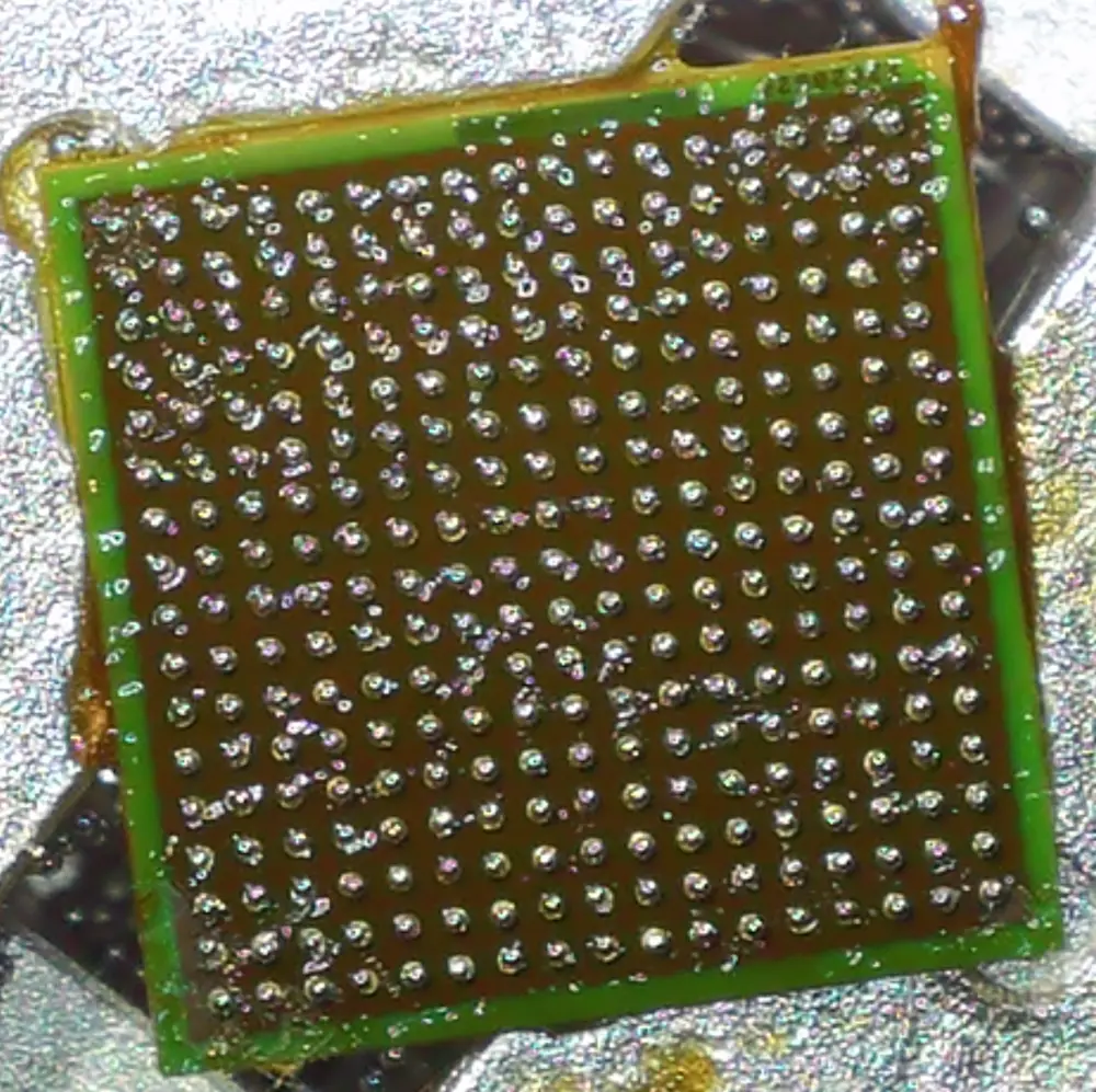
Balls are placed.
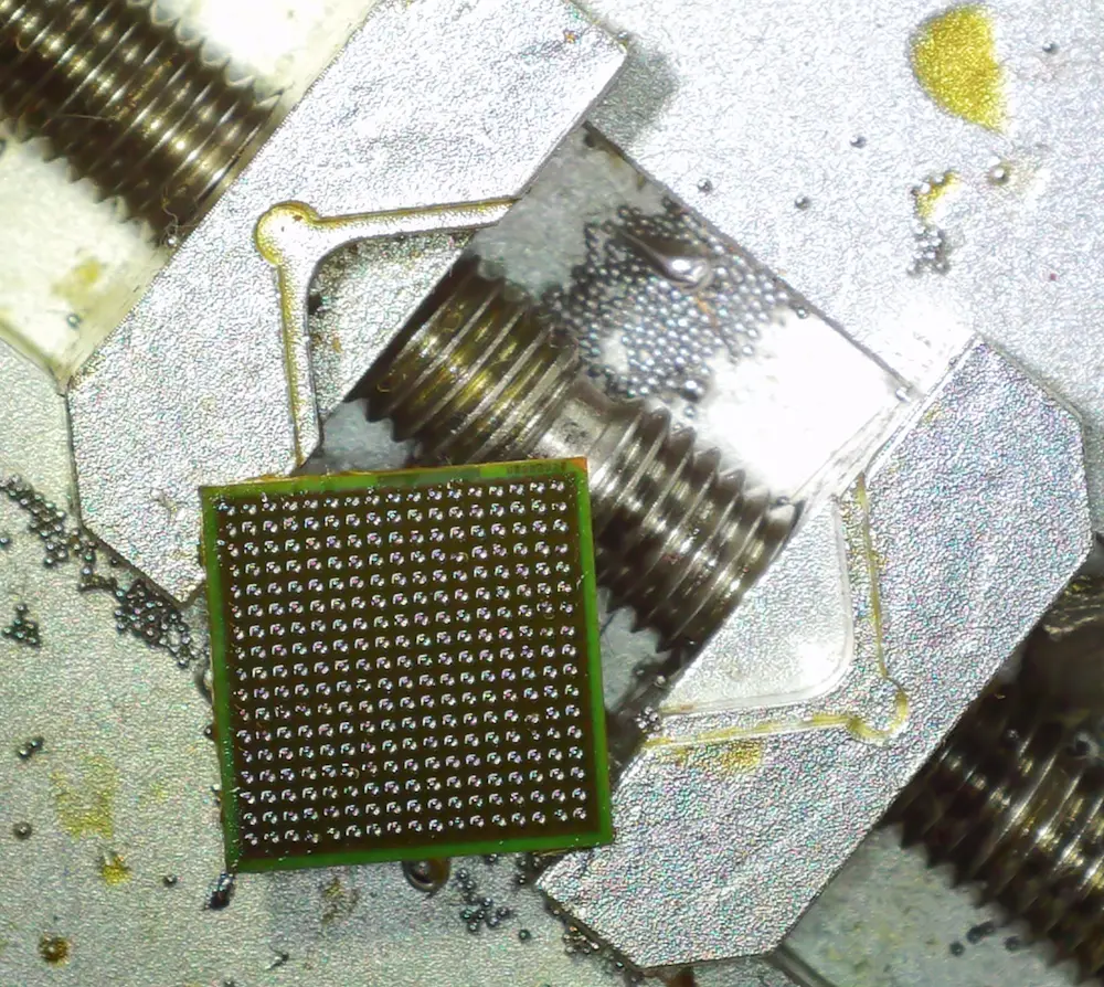
Had to take the CPU out of the jig as it was soaking up all the heat, not letting any of the balls melt.
So now I had a reballed CPU and GPU HW2, all I needed was to plonk them onto the PICO, heat it up, and boom, I would have a working Wii, right?
I checked the resistance on the PICO first, just to be sure… and found that the 1.8V rail was shorted… I checked a few things, but I had my suspicions on the RAM. I had not used flux when I soldered it, as I had not realized how important it was to making the solder balls wick into place, and it had not had the same jiggle when I poked it. So, I removed it, cleaned up the area, checked the resistance, no short, fluxed up the area, and placed down a fresh RAM chip. It went into place a lot better, and I didn’t have any shorts anymore. However, the area under the RAM has started getting a bit scratched up from the solder braid...
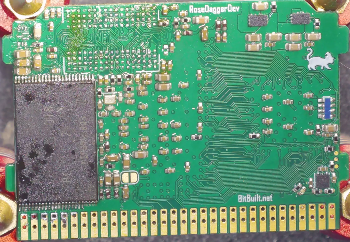
With that fixed I moved back onto the CPU and GPU. I had prepped the area before hand with leaded solder, then removed it with solder braid so that there was only a thin coating on all of the pads and fluxed it up. Then I carefully placed the CPU and GPU down, aligned them, and placed the hot air nozzle above them. The nozzle was big enough that it would hit both at the same time, and honestly the entire board as well. I blasted hot air, while squinting in from the side to look at the GPU to see if I could see with my eyes if the GPU seated down. Then after a while I did my poke test… First poke, nope, not jiggling… Second poke, nada… Third poke, oh there it jiggled the way it does when the balls are melted, great. I just need to remove the heat and look at my amazing creation.
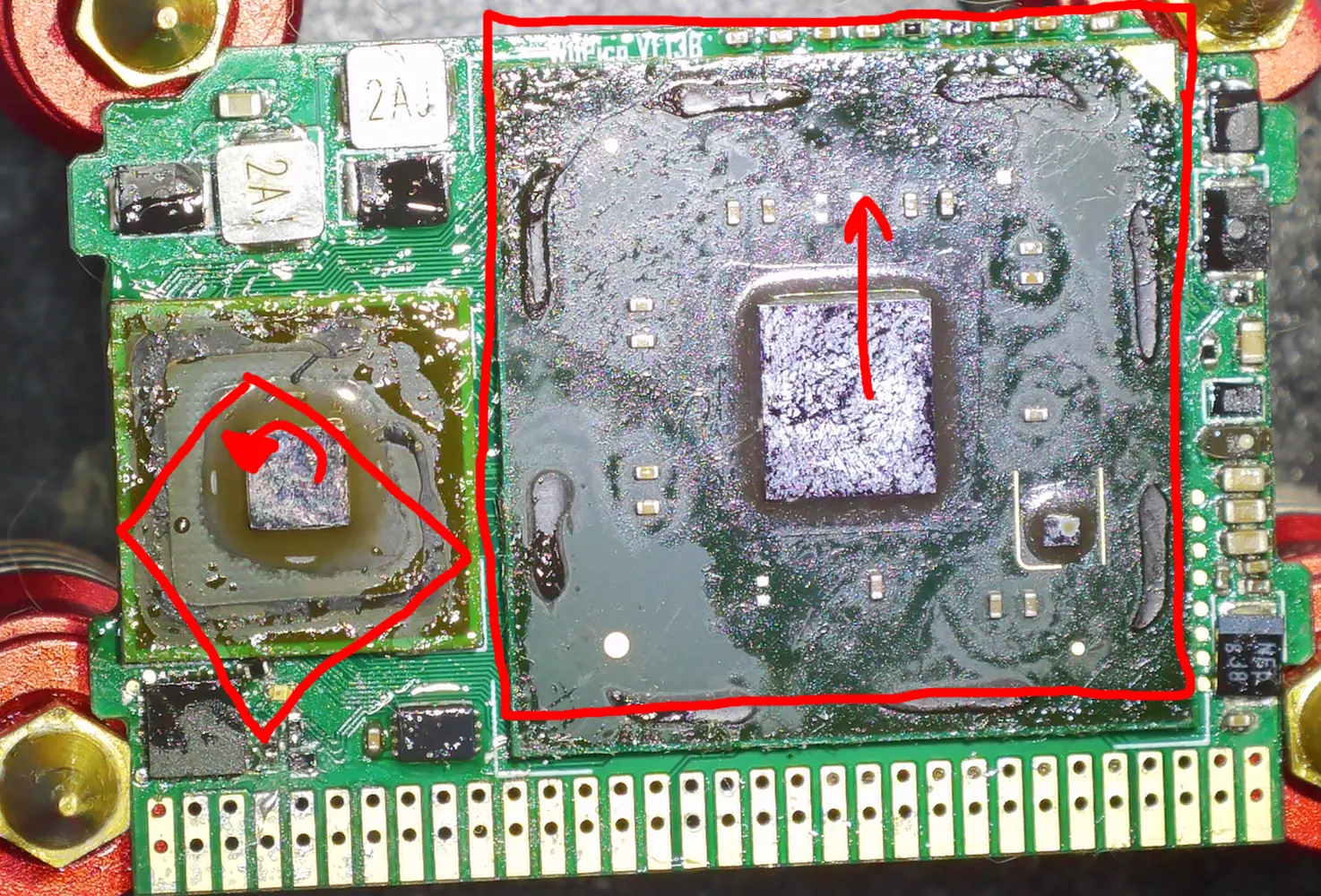
I don’t have an image unfortunately, so I drew how it looked. It seemed like my poke test had pushed the GPU back over a full row, and I had no clue at the time how the CPU ended up completely skewed… So, I immediately place the heat back on, removed the chips, and fixed all the components which had gotten moved back into place.
Hmmm, that went less amazing than I had wanted… But oh well, I’ll just try again! This time I’ll do just the CPU first, then get back to the GPU.
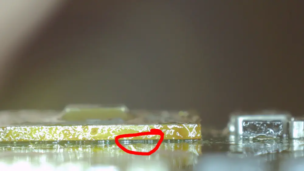
A few hours of babying the floating solder balls, and I had a CPU ready for attempt 2. I used plenty of flux on the PICO and used a smaller nozzle so I could better see what was happening. I heated it up, and suddenly the CPU starts moving randomly! The flux under it started boiling and gassing off, and it pushed the CPU around! That’s why it was all skewed last time! I try to correct, nudging it back into place, but the transplant felt dodgy at best… But not wanting to spend more hours reballing, I decided to move my microscope around to look in on the sides of the CPU, to see if the solder balls looked fine or not. I have good access to two sides, and bad access to the two others. And after careful analysis, I found what looked like a solder bridge on two of the data pins…
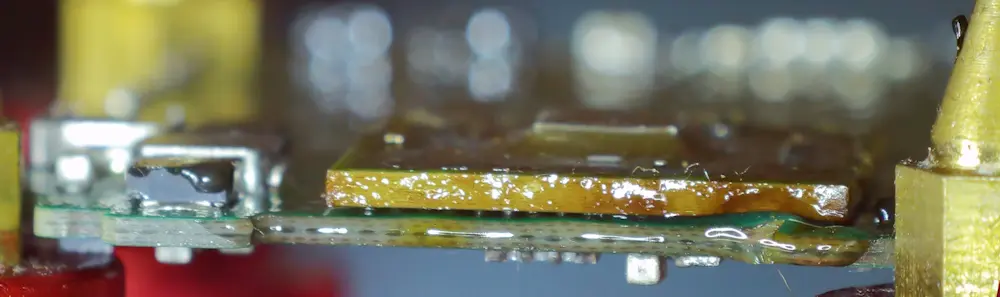
Well time for attempt 3. You know the drill, a few hours later and a lot of frustration, I was ready to try again. Last time I had way too much flux on the PICO, allowing it to literally boil and move the chip. So, this time I used a lot less. Then carefully lined the chip up, before moving my scope around to look in from the side. Now I don’t need to squint from the side to see if they melt, I can just look at my monitor to see when they melt. Brilliant, why didn’t I do that from the start? Right cause it’s a headache to move the microscope arm around and readjust it, and I didn’t think I needed it…
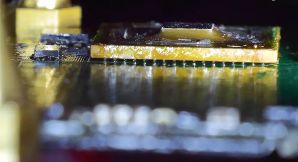
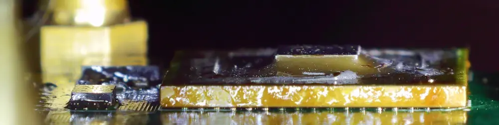
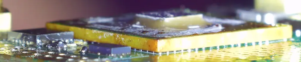
Anyway, I heat it up again, carefully watching that the alignment stays correct, and watching the feed from the microscope, and I can see when the balls start to melt, and how the chip settles straight down, no sideways movement! I don’t need to poke it to check!! I heat it for a while more, just to be sure the other sides and the middle are also fine. Then remove the heat and carefully analyse each side I can see from the microscope. Every side looks golden! Well seated down, good squish, no bridges, chip is square, and the resistance is good!!! I did it!!!!
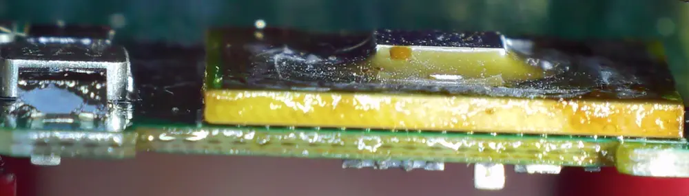
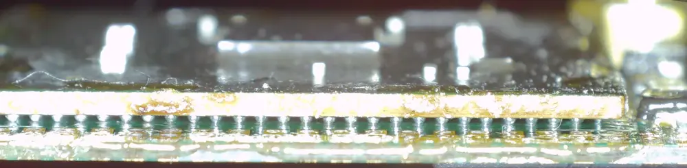
Now the GPU… It’s way larger… I wait till the next day to get started on it, and it takes me the full day to reball it… It wasn’t that hard the other times I tried… I know I use too much flux, and I would save my sanity if I used less. But it felt safer, and I’m stubborn enough that I can handle doing a very annoying task for hours as long as I feel like I’m making some progress… Anyway, many, many, many hours later I’ve successfully reballed the GPU, now I just need to echo the same procedure I did with the CPU. A thin layer of flux on the PICO, place the GPU down square, change the microscope to look in from the side, then heat it up till I can see the balls melt on the microscope. And it went just as well as the CPU!!! Whoop!!!! I just need to analyse each of the sides.

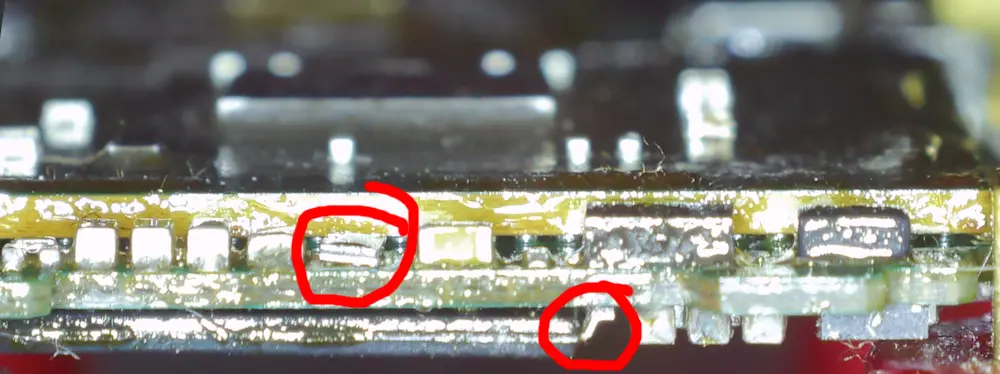
Hmm the 3.3V buck boost is clearly not positioned well, it’s a micro-BGA component, but I have a replacement. And the NAND desoldered itself.
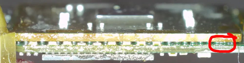
Hmm is that a damn solder bridge? How? It didn’t move! There were no bridges when I place it down… Damn it… But lets take a closer look just to be sure.
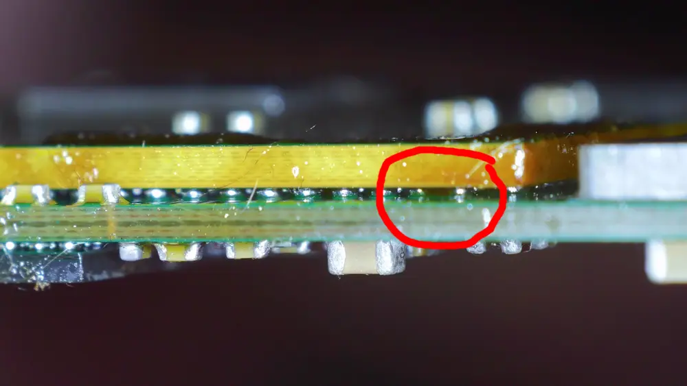
Hmm from an angle the bridge disappears and it looks more brown than metallic… It might just be flux… Let me check what pins that’s supposed to be… I know there’s a lot of ground in that area. It’s Ground and 1.15V… Let’s check resistances… Not a short! The resistance looks fine! Let’s check the other rails as well… They are also fine! Maybe I did it?!
I just need to fix the NAND and the 3.3V regulator and I can finally test the PICO. We are almost there! (Don’t look at how much is left in this work log…)
3.2 I HATE micro-BGA!
So, I used the same regulators as the ThunderKILL which used the same regulators as the ThunderVolt, which used a tiny micro-BGA buck boost for 3.3V. These micro-BGA components use balls that the size of a needle point, and the pad’s are not any larger… I had one unused backup of this regulator, so I heated it up to remove it… The regulator would not budge… I keep waiting for it to heat up enough… But the point never comes… I up the heat on my hot air, and finally it want’s to come free. So, the solder balls they use are apparently very high heat… I clean up the pads and put some flux down, then place the regulator down and start heating it. The silk screen outline around the chip is taller than the balls, so I can’t really look in from the side, though I probably should have tried. I heat for a good long while, at a higher temperature than normal, just to be sure the high heat solder balls will melt, and I don’t poke it. Once it felt like enough, I let it cool down, then poked it to see if it would stay or if it would come loose. And it stayed in place, so some of the balls stuck down at least.
I connect up the wires for the ATTiny, so that I can flash the firmware to it, and do some modifications to make the ThunderVolt firmware fit the picothunder (I used some different pins and components, and moved the LED, the Thundervolt has a dimming LED, I don’t as I didn’t realize the LED pin mattered, or that that was a feature). Once that’s done, I connect the test dock I made and give it power.
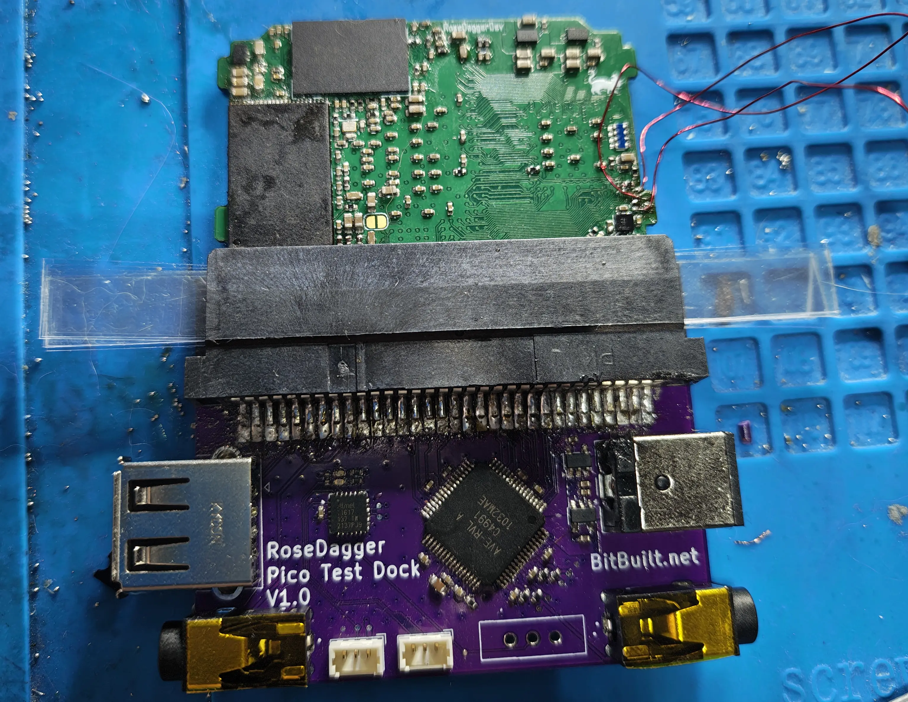
The plastic bits are there to make the PICO thicker so it will press into the contacts properly.
On the Thundervolt, the LED will breathe when everything is fine, and it will flash an SOS if it fails somewhere. My version will blink regularly if everything is fine or do the same SOS if something wrong. I check the LED, and it’s blinking steadily. Great! Awesome! This is really coming together! Let me just check the voltages to be sure. 1V? Yes! 1.15V? Yep! 1.8V? Right on! 3.3V? Hmmm… why am I getting 0V on 3.3V? That’s not great… Let me check the code again. Hmmm it will SOS if it can’t find and can’t talk to the regulators. But it never checks the voltages, or what the regulators has to say. So, the 3.3V reg is present, is answering I2C, but is not converting… Hmm, let’s look at the datasheet for that regulator, let’s see what status registers it has, I’ve use different regulators before which had a lot of telemetry and status I could access. Hmmmmmmmmmmmmm… It only has Power Good, and Temperature Good… Let’s check those… Okey it’s reporting Power Not Good… Great it is aware it is not working, but won’t tell me why…
I double check that the inductor I have has the correct ratings and that I didn’t mess up the size of it. The datasheet, and the ThunderVolt Schematic says 0.47uH, checking Digikey, the inductor I ordered was a 0.47uH inductor. So, it seems fine. I keep checking some more stuff, but it feels like it mostly comes down to the regulator, which has those cursed micro-BGA pads, and maybe it’s not fully seated, or something is wrong with the inductor… The inductor is easier to replace so I do so. I add a bit of fresh solder paste just to be sure it will stick down, the solder which is there currently has been heated and cooled a good few times now. I heat it up… And the solder paste starts spreading around as it becomes more liquidy… And some of it goes under the regulator… Just absolutely perfect, that’s exactly what I wanted… Fresh solder getting stuck under the micro-BGA regulator that I don’t have any spares for… I check just to be sure… And the switching pins and vout are shorted…
So, I desolder it… clean up the solder… then try to reball it using the solder I have. I tin the pads on the regulator and on the PICO and try to get them to merge. SOS the Tiny can’t talk to the regulator… Off with it again… Only tin the chip and not the PICO… Hey it’s talking again, and I’m getting some voltage on the 3.3V rail! 0.5V is some voltage… but not the right voltage… I’ve been probing the everything with my oscilloscope, both before I had to replace the regulator again, and after, and it never properly converts. On the 0.5V it tries to convert for a little bit, then gives up… And so do I…
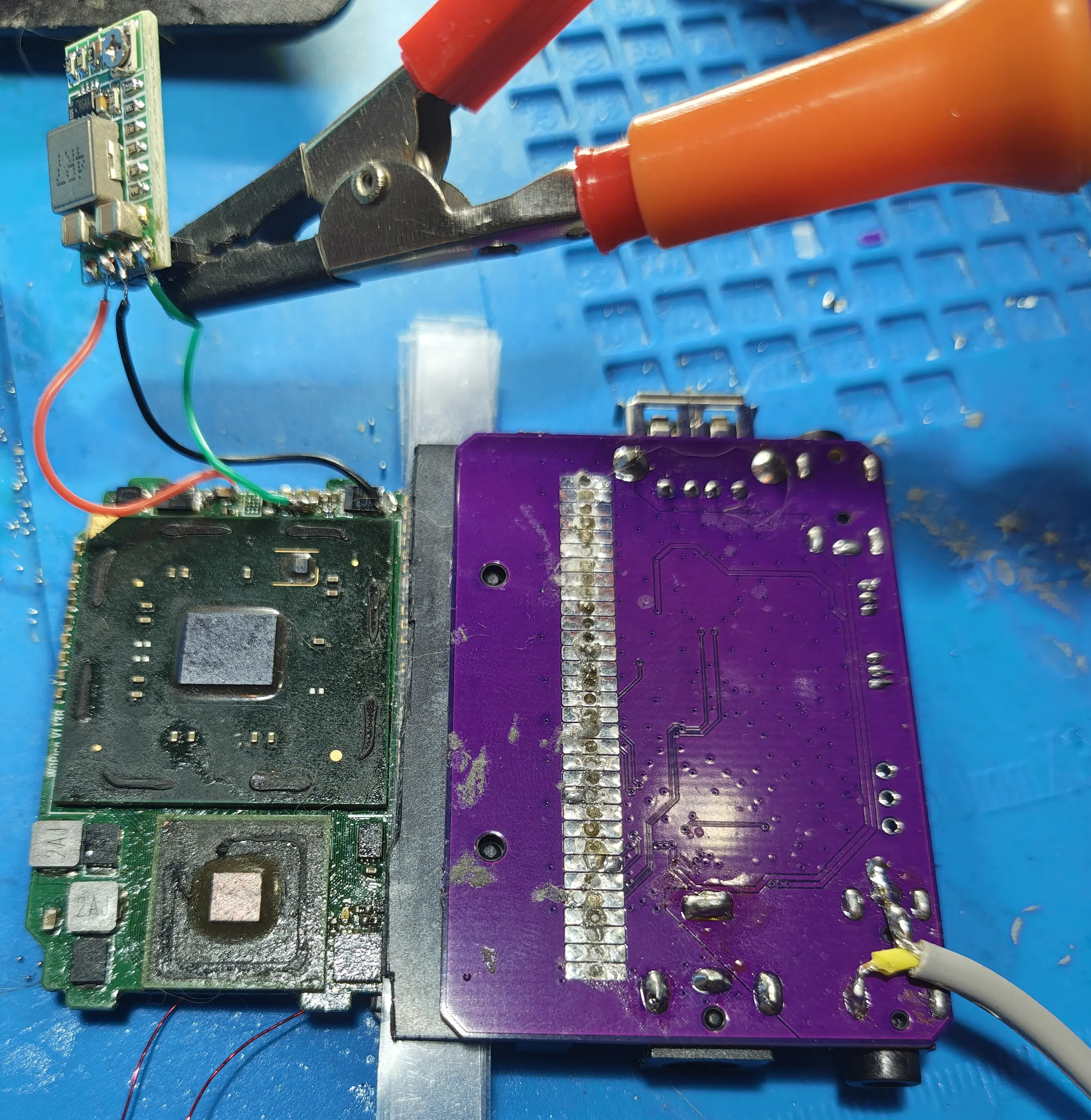
This 3.3V micro-BGA regulator is the bane of my life, I just wanted to see if the PICO would work, why does it hate me so much? Fine, I’ll just get rid of it, and replace it with an external regulator, I have a few of those laying around. And I swear for the future to never using micro-BGA for any projects I need to solder myself ever again!
I change the firmware to not look for the 3.3V regulator, then I try one regulator I have. Out of circuit I adjust it to 3.3V, then solder it in… The 3.3V rail is only supposed to draw about 0.25A, so it’s not massive, surely it can handle it… Nope… I don’t get the voltage I need… Fine I have another slightly better regulator that I’ve use before which should work. I solder it in, adjust it, aaaaaaaand 3.3V!!!!! I check the other rails, AND…. They are still good!!!!!! It’s alive!!!!!! Mwahahahaha!
3.3 Pico Debugging
With all the power rails operating, I just need to attach the video out to the dock, and check my monitor, surely it will be that simple right?... No image… Fine let’s check some stuff. The CPU and GPU both heats up when connected to power, so they are doing something. The debug port is outputting 0x80… It’s a solid 3.3V and that’s not a valid code… Okey let’s check the video out pins, which feeds into the AVE. The 54MHz clock should be reliable, that’s reading 27MHz…. Hmmm that’s not right… Let’s check the data pins? No activity… U10? Hmm the only place I have access is a tiny via right next to the NMOS. So I carefully scratch the solder mask off and probe it. Oh, this is not correct, it’s going high while the 3.3V regulator is still booting, maybe the external regulator is taking more time than the intended regulator. But that is an easy fix, just need to change the firmware of the Tiny to extend the delay.
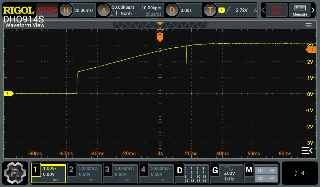
Hmm I’m seeing the same behaviour… Let’s delay it further… Nope… a 2 second delay? That’s something I should notice, is there a 2 second delay from plugging in power, till the signal is captured? Nope it’s instant! I check the LED, that gets delayed from blinking by 2 seconds, so the Tiny can keep time… Maybe the NMOS isn’t soldered properly? It’s another very tiny component with very tiny pads… And sure enough, the gate and source pins were not wetted… Okey let’s resolder it… And probe it…
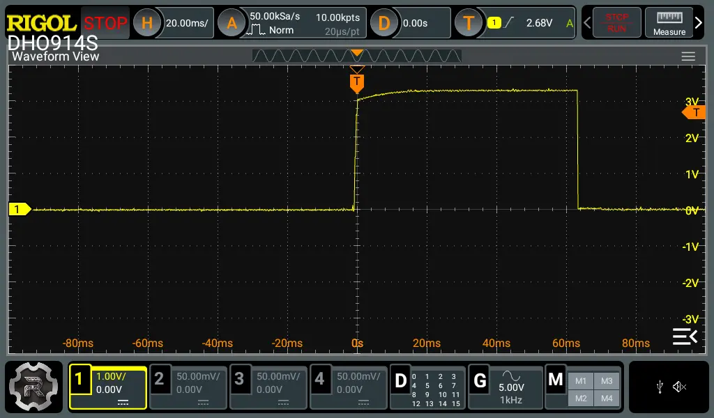
Oh, it turns on initially, then turns off as the Tiny wakes up, then turns on again after the delay. The 3.3V regulator is not connected to the enable line for the other regulators, so it just boots as soon as it gets power. But at least the delayed U10 reset is happening now, after the rails has fully powered up.
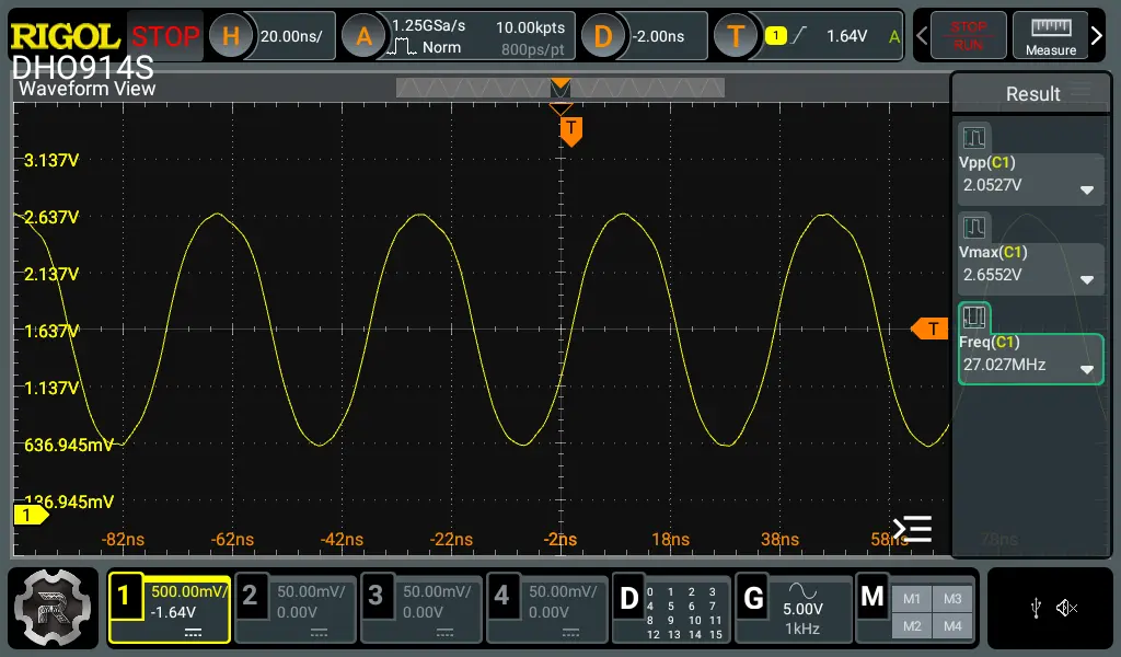
Checking the 54MHz video clock… Still 27MHz… Okey on to the next issue. Let’s check the clocks around the board, first checking the stock Wii, aka Foxtrot. Okey the main clock is supposed to be a 27MHz sine wave centered around 1.8V. The CPU clock is a 243MHz sine. Let’s check the PICO. The main oscillator is… Flatlining… That’s not good…
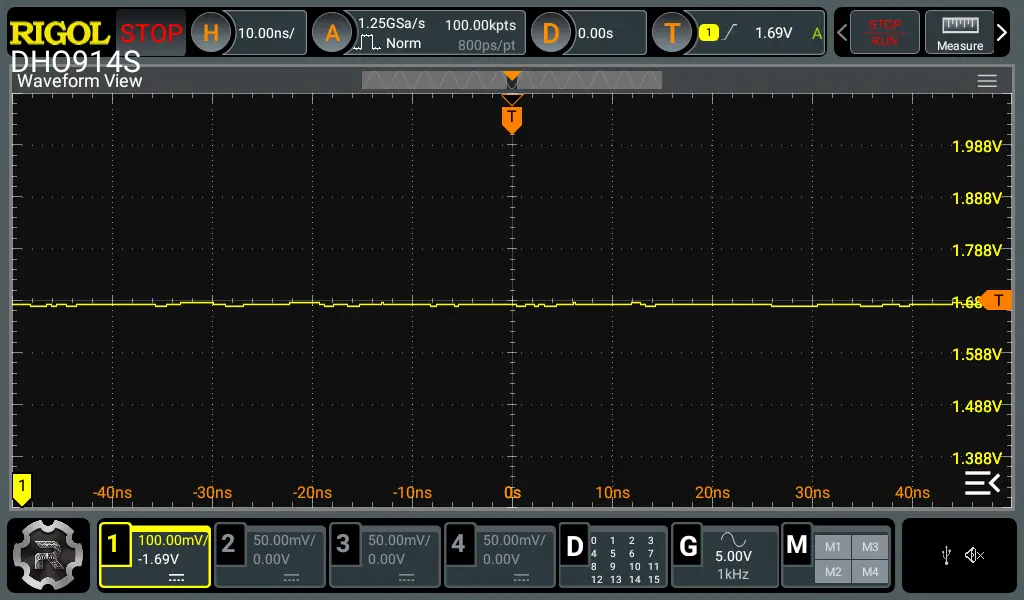
I try to reflow the area. Nope. I try to replace the load caps assuming there is less stray capacitance than I did for my first calculations. Nah. Hmm, the probes have have a 1x and 10x switch, 10x is for more sensitive and small signals, but I’ve never really used it, and didn’t need it for the stock Wii, but I replaced the crystal with a smaller one… Let’s see what happens if I change mode… Oh there is the sine wave, 27MHz just as expected.
Okey according to this, the CPU is supposed to be 243MHz and the RAM is supposed to be 486MHz
Let's check CPU clock... 237MHz! Great, close enough! The GPU and it’s clocking and PLL systems are working! And the CPU gets an appropriate clock.
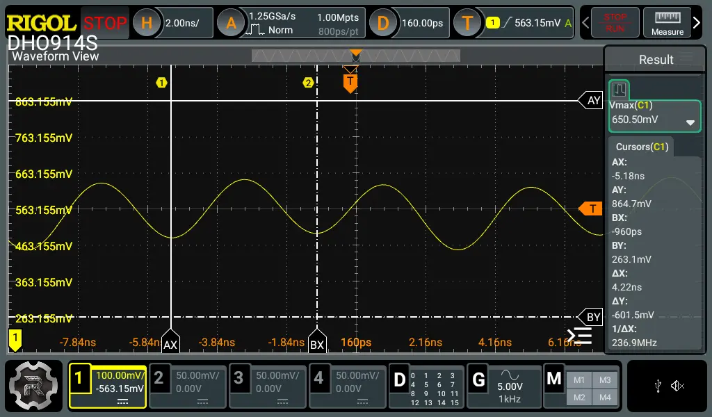
Now let’s check the RAM, most of the traces are hidden under it and under the GPU, but I have access to the terminating resistors for the clock, which is supposed to be 486MHz. And I measure… Garbage… centred around 1.8V
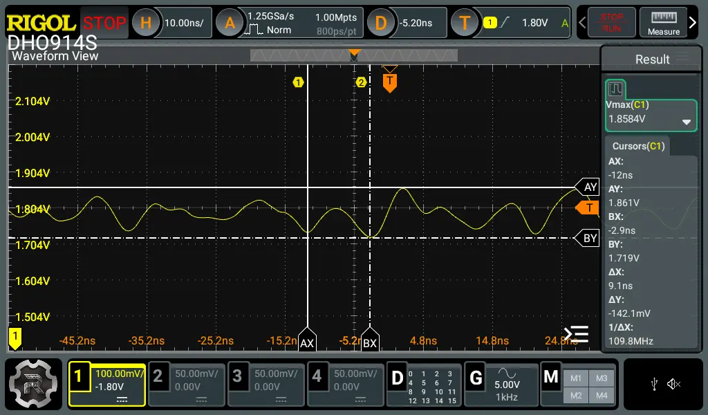
Well that’s not what I want to see… Let’s check to stock Wii… Hmm I’m seeing something there, but it’s not very clear… What’s going on? It’s centred around 1.3V…
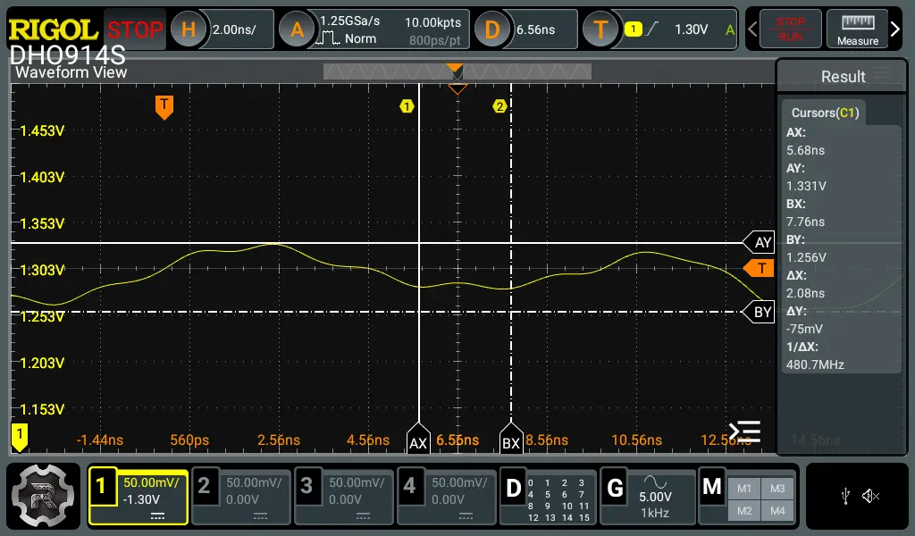
Why is the signal on the stock Wii so weird? Hmmmmmmmmm…. My Rigol DHO914s oscilloscope is rated for 125MHz… the DHO924s is rated for 250MHz, and uses the same hardware, just a different firmware… Those who are good at math might have notice an issue… 486MHz is slightly larger than the 125MHz or even the 250MHz that my scope is rated for… XP Though I could at least see something of the waveform for the 486MHz on the stock, even if it was very distorted. The PICO is not even showing that…
I checked the Vref for the RAM, which is supposed to be 70% of VDD, which it was, for both the vrefs.
Also checked there is no activity on the datapins for the RAM.
I'm not sure what else I can poke to investigate...
Next step might be to desolder the RAM again? It was hanging upside down while I was soldering the GPU so it might have started to desolder itself? Though it looks fine from the outside...
There is also the risk that the scratched solder-mask under the RAM is causing issues and something got bridged? Though then I either need to get lucky when I solder a new chip on that it does not short... Or start over on a new board... Which would be hell, I don't have a lot of backup components, so I would have to order more, or harvest from the current board...
Or me moving the DQ groups around messed it up so much it wont initialize? Or the interference from the compact traces makes it give up and not not initialize? But I would expect the 0xF1 boot code if the GPU came alive enough to test the RAM and it failed. So it fails before even reaching Boot0...
Maybe the RAM is a red herring and it's showing no activity as the GPU has not tried to initialize it? But then what else might be wrong to the point the GPU does not even reach Boot0? And never tried to initalize the RAM or start the RAM clock?
And that's about where I am. Unsure of what is wrong or why. And mostly poking and prodding stuff to see what behaves as expected and what does not.
4. Postamble jabber: The reality check I want to ignore
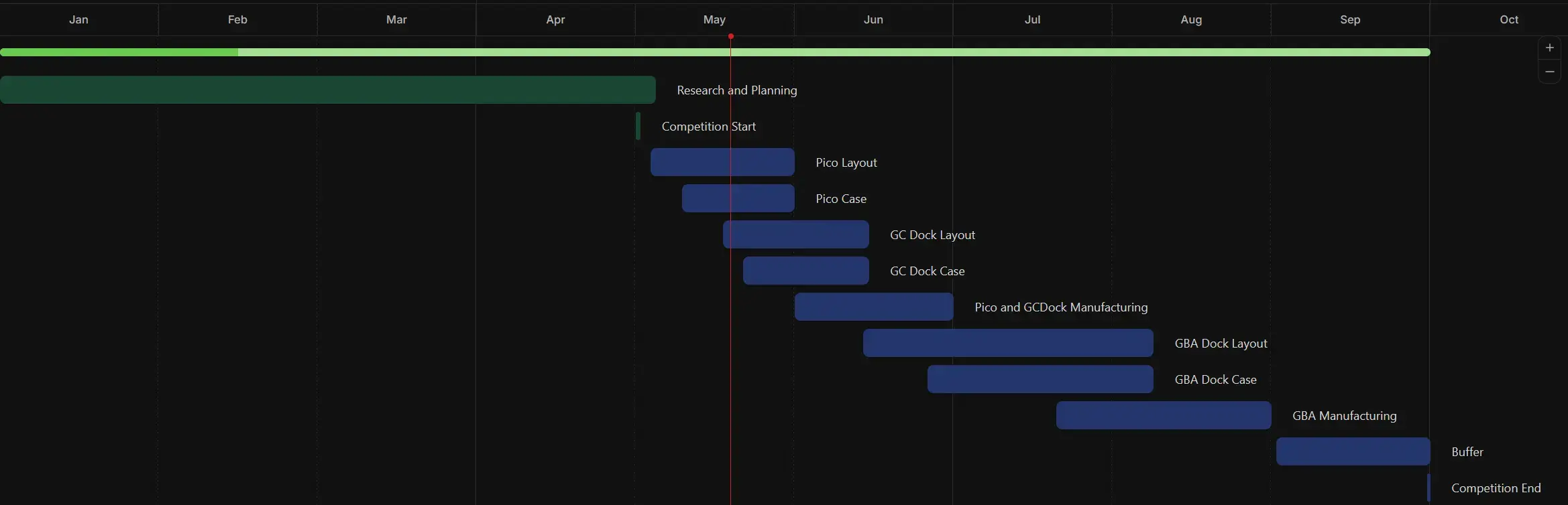
So, when I started this project, I set out a few goals and made a rough gantt chart/timeline to see how much time I would have for each step. I had planned to update that chart as I went, but of course I kept forgetting about it. But now, with two months left, and having lost one and a half months to trying to get an HW2 GPU I could use, it might be time to return to that overall plan.
As Loopj said in the discord:

Which is true, but at least for me, it gives me a visual indicator of how much time I have left and what is left to do in that time, so I made another one, updated to how things actually went.
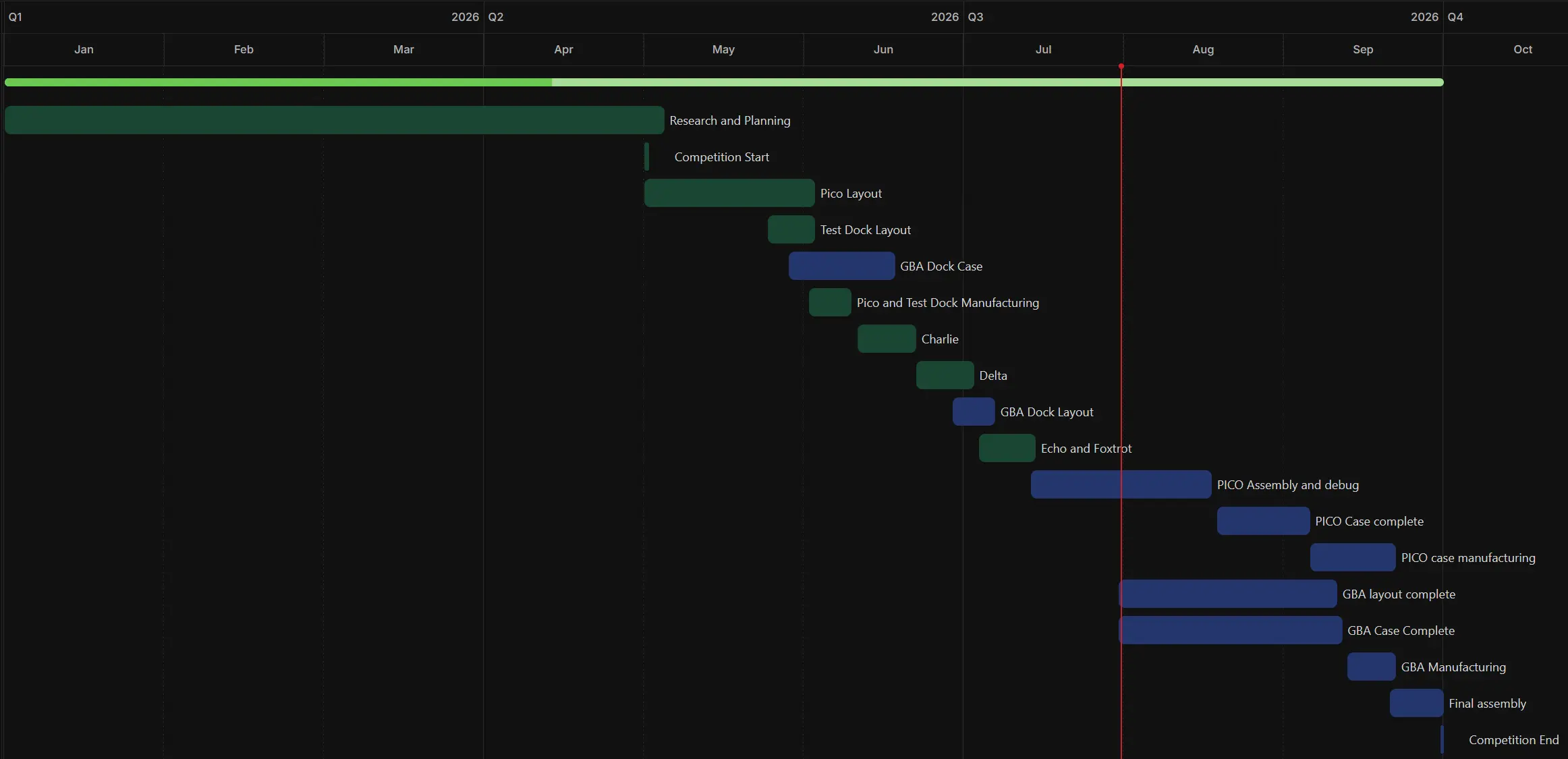
As you can see, I failed to deliver on most of those shaky promises, and the full month buffer I had made is completely gone. There might still be a small chance that **IF** I get the PICO working in the next week or so, I **MIGHT** be able to finish, as long as I don’t need to do any reprints or revisions… Something that I failed to accomplish last year…
Of the original goals I had I’m going to have to cut down on some of it to have any chance. Mainly the TV Dock. I don’t have the time or motivation for it. It was supposed to be my shot at the smallest Wii ever made, smaller than the Kawaii, but I had no ambitions or wants for it beyond trying to claim that title, so it’s best to just… not do it. I’m also not gonna mess with MIPI and just stick to the HDMI driver board which came with the display I got.
So, my current goals look like this:
Main goals:
Anyway, think that’s enough for this update, I’ll try to not wait as long on the next one, and make it slightly shorter than this monster update I just really, really, really wanted to get to the promise of last time, either have a working PICO or debugging it... I won’t make such a promise again. But let’s check Word just for fun, without images I’m at 15 pages, ~7500 words. If you read all of this, congrats and thank you, I spent way too long writing this XP Time I probably should have spent on debugging…
Heya, so maybe it’s time for another update, it’s only been, let me check… a month and a half since the last one XP
So very little and a lot have happened in that span, but to pick up where we left off last time where I said
Maybe I'll have something booting in the next one, or I'll be deep into debugging and learning from potential mistakes XP
I’m definitely in the latter of those two options, and if you are interested mostly in how that’s going, you can skip to the debugging section. Otherwise let me take you through the meandering path of trying to get good chips to harvest.
Note from later me, this entry turned very, very, very long, I’ve split it into sections:
- Preamble jabber
- The quest for HW2. Aka the journey to harvest working chips
- The adventures of Chipped Charlie
- Brave Bravo
- Disappointment of Delta
- Echo and Foxtrot, an encouraging chance to fix this mess
- The big quest for a tiny PICO. Aka the journey to make the PICO work.
- Why the fuck did reballing get more difficult again?
- I HATE micro-BGA!
- Pico Debugging
- Postamble jabber: The reality check I want to ignore. Aka where am I, where should I be in this project, and how much/little time is left…
2. The quest for HW2
2.1 The adventures of Chipped Charlie
So last time I had just gotten the PICO boards, and started soldering it up, and had a regular Wii with a HollyWood 1 that I had planned to use. But I got convinced into ordering a Wii mini so I could get a HW2 which uses less power and has better power efficiency. For a tight build like mine it made sense, though it would delay be a tiny bit having to wait 2 weeks for the Wii mini to arrive. Looking back with hindsight I should have used the HW1 I had as an experiment to see if the PICO worked, then worried about the HW2 later… But it was only a 2 week wait, so I could work on the 3d model for the GBA case, no biggi.
So, the first Wii mini arrives, however, before anything else, I’m going to give it a name, I already have a few Wii’s laying around, and spoiler, I’ll get a few more. Names will help separate them.
- Alpha – The first regular Wii, which is the one I cooked dead
- Bravo – The second regular Wii, that I got, but didn’t use as I wanted a Wii mini.
- Charlie – The first Wii mini, the one I’ll be detailing in this section. (Also sorry for anyone name Charlie here…)
So, I check that Charlie boots, install RVLoader like I’ve done on a half dozen Wii’s before. Then bake Charlie. Unfortunately, I don’t have a PCB oven, so I decided to use my preheater. I put Charlie upside down on the preheater, so that the CPU and GPU gets baked, and let him sit for 6h. I was recommended 100C for baking, and using some temperature probes, I saw that there was about a 20C difference between what the preheater was set to, and the board temperature, so I set the preheater to 120C, so that the board was 100C.
After those 6 hours, I flipped Charlie around and baked him for another 6 hours the right way up. I really didn’t want to take any chances after the last board, Alpha, turned out very very very very very dead.
Once Charlie was sufficiently baked on both sides, a full 12-hour process… I started bringing him up to temperature. Last time, with Alpha, I did it right after being sick, and had a massive headache, and rushed without thinking and without checking what was reasonable, even though I had harvested chips from PS3’s a few times before then. So, my dumb brain had done the dumb thing of: “Well I set my soldering iron and hot air to 320-350C so that’s the temperature I should reach…” Solder starts melting at around 220C… The reason the iron and hot air is set higher it to overcome the heat loss from radiating heat elsewhere, and to overcome the losses from needing to heat up the ground plane and pcb acting as a heatsink… I reached a bottom temperature of 290C… which is slightly above the solder melting point of 220C… Delaminating Alpha, making it go all discolored, delaminating the GPU, and components on the bottom side had just fallen off due to gravity… So that was slightly sub optimal…
This time, with Charlie, I checked… A reasonable bottom temperature is 180C, then you bring it the rest of the way up with hot air and start checking if the chip is floating once the top probe reads 220C. The technique I ended up using was holding the hot air nozzle very close to the GPU, counting to 30, then gently poking the GPU with a tweezer that I gently held in the far end. If the tweezer bent, then it was not ready, if the GPU moved, then it was floating, however I let it heat up for another 30 count, to be sure it was fully floating and that I was not ripping any pads, and that it would not solidify as I removed the heat to lift it up. And that seemed to work well, I got the GPU and CPU and RAM off without issue, there was no popcorning on Charlie, and checking the resistances one the GPU and CPU they turned out fine. (I’ll post about the resistances in a later segment.)
However, I was not yet quite done, so after spending 12 hours baking Charlie, then more time carefully heating him up to temp slowly and harvesting the chips, I decided to do the next step right then and there before going to sleep. Because the best work you do is while tired before going to sleep… So, what did I need to do? Well since I needed every fraction of a millimetre of space for the PICO, I needed to delid the GPU and CPU, so their height would be slightly smaller… So, I did as last time, I took a razer blade and carefully cut the glue around the edges of the IHS, making sure to angle the blade slightly upwards so it would not scratch the substrate. I did the corners first, careful about not going too far in. Then I did the edges. Then after working it for a bit, the IHS popped off, and I could see the silicon die, and the caps around it, and the tiny silicon die which others in the discord identified as the EEPROM. Everything looked great! There were no popcorning visible, no scratches, no defects I could see. So, I posted it in the discord, and we looked at some of the differences between the HW1 and HW2, along with the empty slots for caps. Then just as I was about to sign off, Rob noticed something, a potential defect, just from the image below. Can you spot it before I point it out?
If you zoom in to the EEPROM, there is a slight discoloration which looked off to Rob.
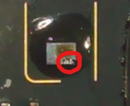
So, I took the chip out again, and adjusted my microscope to try and get a better image… and fuck me sideways, he was right… A tiny piece of the EEPROM had gotten chipped…
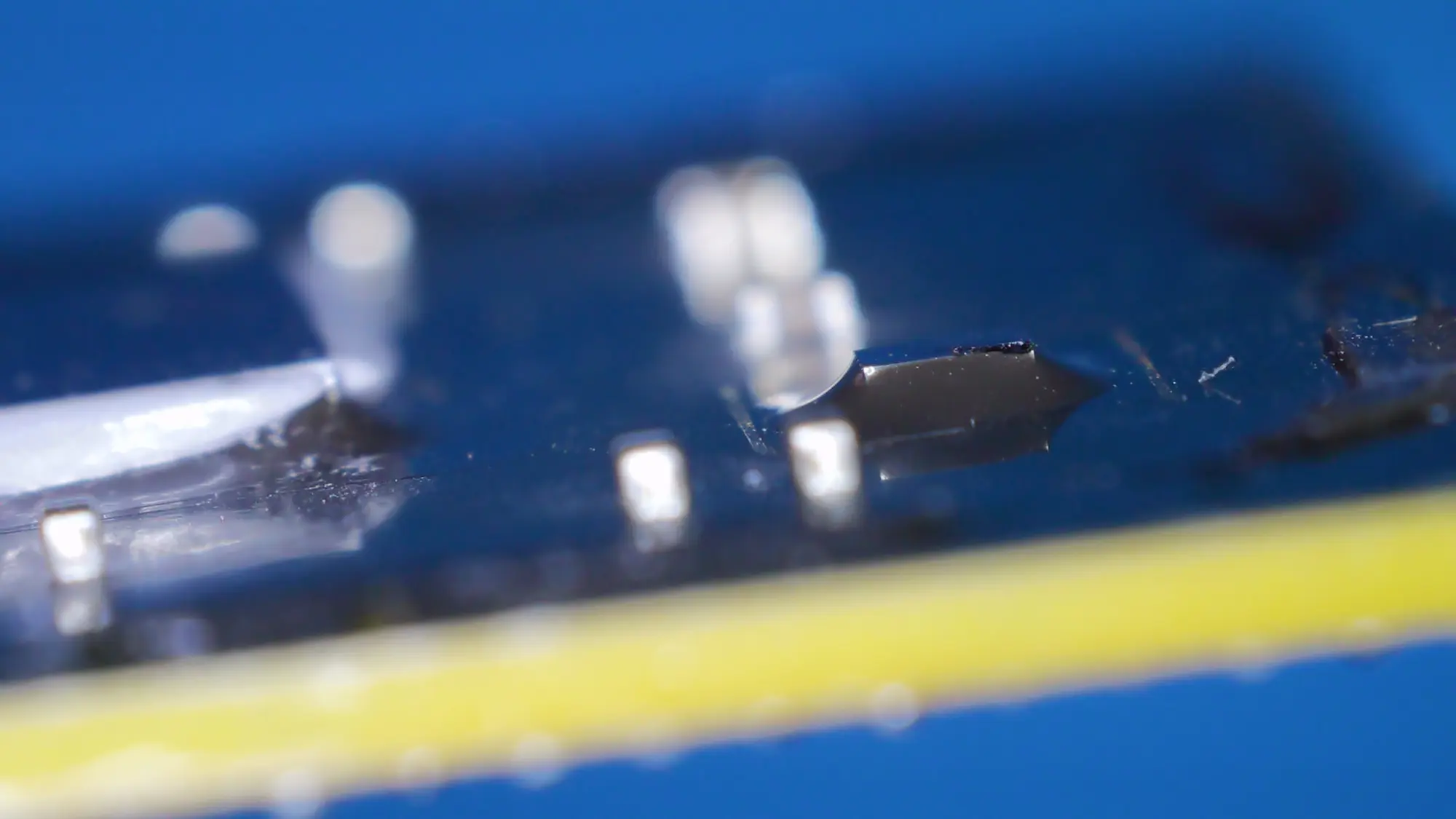
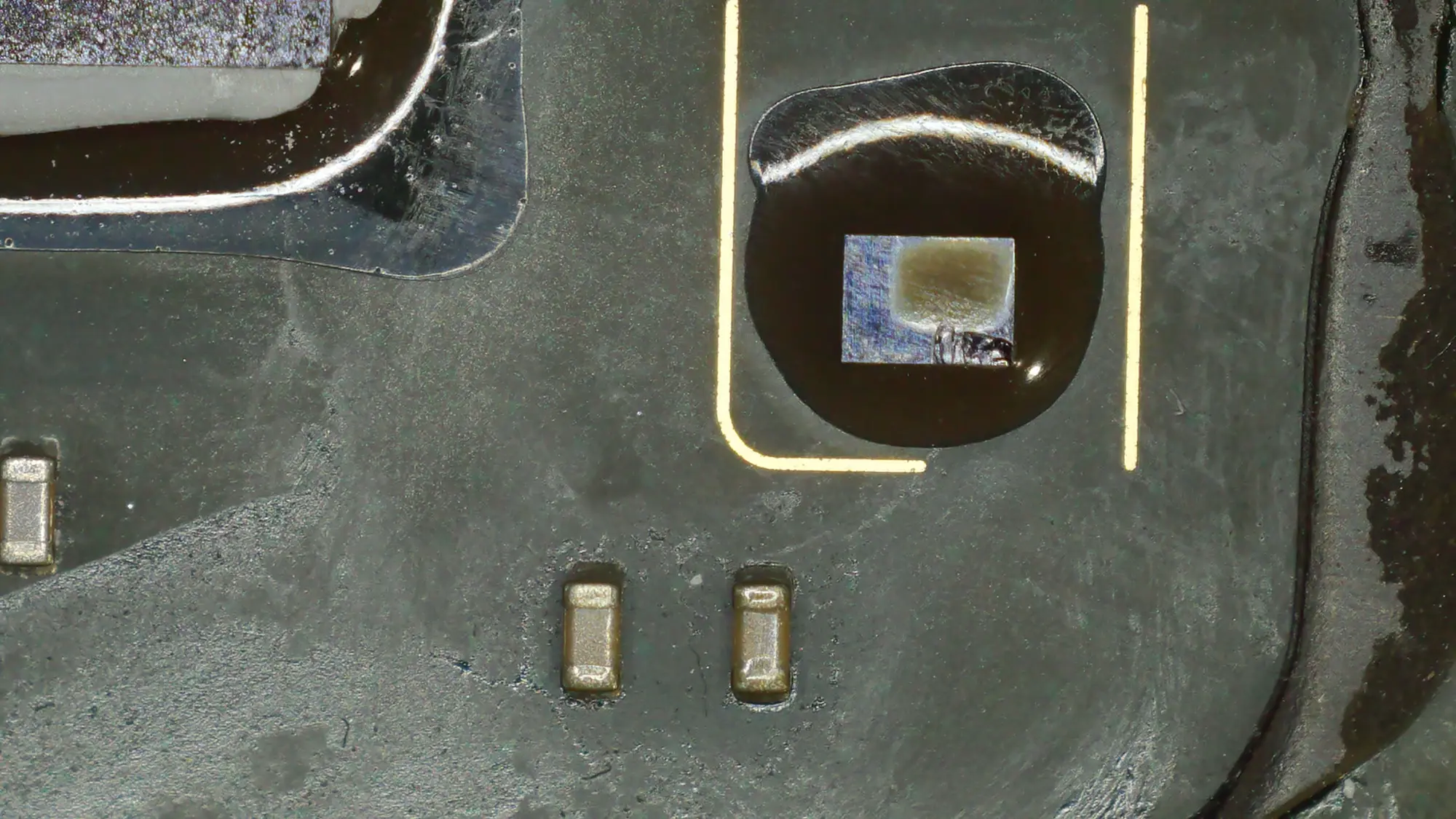
It’s shallow, but it might have taken out something important…
So, I took the chip out again, and adjusted my microscope to try and get a better image… and fuck me sideways, he was right… A tiny piece of the EEPROM had gotten chipped…
It’s shallow, but it might have taken out something important…
So, the HW2 from Charlie was potentially dead, and the only way I could check was to test it… But I had just removed the GPU, CPU, RAM, and NAND from Charlie, and I really didn’t want to put them back on. Though from the discord I got the suggestion to put the GPU onto the working regular Wii I had, aka Bravo, though as the NAND and GPU are married to each other, and I didn’t dump the keys, I needed to transplant both. Though as it was Sunday, and I had work the next day, and baking takes a long time, I needed to wait till the next weekend. There was also a risk in transplanting the GPU, as according to Rob, the vias on the stock Wii makes it difficult to transplant a GPU back onto a stock Wii without creating bridges… You need it to sit perfectly and not shift… So, it was mostly a hail Mary (good movie and better book btw) to see if the HW2 from Charlie was still good. So, I ordered a second Wii mini (Delta), just in case the HW2 I had from Charlie was dead.
2.2 Brave Bravo
During the week I had, I spent my afternoons practicing reballing on the very dead GPU from my first attempt aka Alpha, and I got better and better at it. The first proper attempt. I had about 10 solder bridges (error image not found). My second attempt I had 1 solder bridge, which merged into a big ball, I tried to rescue it with solder wick but just made a bigger mess. My third attempt I had issues with the balls not wicking down, so after I was done, I found several balls who were not seated, so I heated it up again… and managed to bump into a bunch of the balls with the hot air nozzle… The fourth attempt I used more flux so the balls would wick better. I had to stop a few times as the balls started floating together, and I needed to separate them before they formed a blob, but I got a perfect reball!
Then I did the exact same thing to the to the chipped HW2 from Charlie and got it on my first try!
Then next weekend come around, and I start going through the procedure again with Bravo. Last time I did 6 hours on each side, however as the temperature probes on the top and bottom were relatively close, I decided to do 3 hours upside down, then 6 hours right side up, so it was only 9 hours of waiting on Bravo. Then I bought Bravo up to temp, and started blasting the GPU with hot air, this time being even more careful to not rip pads. It had gone well last time, but I really really needed it to go well this time. I poked it gently till it was floating, then waited a bit longer, then lifted it. No ripped pads! I cleaned it up, using leaded solder then solder braid, before I put down fresh flux and placed the Charlie HW2 down onto Bravo. Then I started blasting it with hot air, waiting till the probe reached 220C, and repeated the same procedure to check if the balls had melted and that it would bouncing back into place. I removed the hot air, and let Bravo cool down, and turned off the preheater. Then flipping the board while it was still hot, I removed the Bravo NAND and placed down the Charlie NAND.
I needed to clean up the legs of the Charlie NAND, but then it was time to see if it would boot. I checked the resistance which seemed fine, no shorts. I plugged in the power, and the power LED turned on. I pressed the power button, and the LED switched color. All great news! So, I kept looking at my monitor to see if I would get an image… No image… I checked the boot debug pins, and I got a flashing 0xF1… Which is EEC or RAM issue… That is step 1 of the boot process… The EEPROM is step 7… Maybe there were some bridges on the RAM side of the GPU… Maybe I had accidentally bumped the RAM chip while transplanting the GPU… I remembered what Rob said about transplants on the Wii was difficult and that it was a long shot unless I got the alignment perfect, and my method to check if the chip was ready was by poking it… My work bench is not big enough that I can have the preheater and the reballing jig out at the same time, so I would need to spend a few hours heating the board up and harvesting the GPU again, then let it cool down before I move the preheater away and try to reball the GPU again, which could take a few more hours, then I would need to move the preheater back and heat it up again, to try and transplant the GPU back… That would take ages… And I had a new Wii coming for the next weekend. So, I cut my losses and put Bravo with the Charlie HW2 aside, I could come back to them late and try again if needed.
2.3 Disappoint of Delta
The next weekend comes around, it’s now 4 weeks since the last update, I got the new Wii mini, Delta, it’s a HW2, I jailbreak Delta with bluebomb, using linux, though it’s very annoying pressing the BT reset button over and over and over and over till it connects. Then once Delta is jail broken and the homebrew channel is installed, I just need to install the RVLoader like I’ve done plenty of times before, with the plan to dump the NAND afterwards. I check the settings and change the WiFi to be patched out, and no VGA patch, and I let it install. It starts the process and everything seems fine, until it freezes at “Exitting…” which I’ve not seen before. Though it looked like it was done, so after waiting a while, I decide to just power cycle Delta, if the update didn’t take, then I could just install it again… I try to boot it… And I get nothing… The power led changes color, but I get no video out… The debug port is outputting a solid 0101 0101 which isn’t a valid code, and it’s supposed to flash (50% duty cycle signal) … I managed to brick Delta… I check the forums and the discord, and there’s been a few people who has encountered the “Exitting…” freeze, but they either didn’t manage to fix it, or fixed it without telling anyone how…
I thought back to how I changed the WiFi settings… Wasn’t the default that it was patched out… Did I patch WiFi in? The Wii mini does not have a WiFi card, the connector is not even added to the board, and the series resistors are also gone…
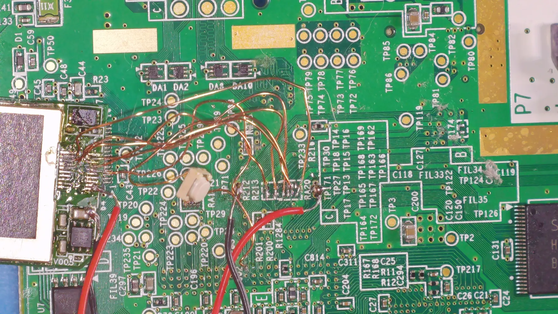
But I have a WiFi card from a regular Wii, so let me follow the guide and install it on Delta on the pads to the GPU just to see if it would work. So, I fiddled with magnet wire for a bit, before I got it soldered up, and I checked… Still no video out…
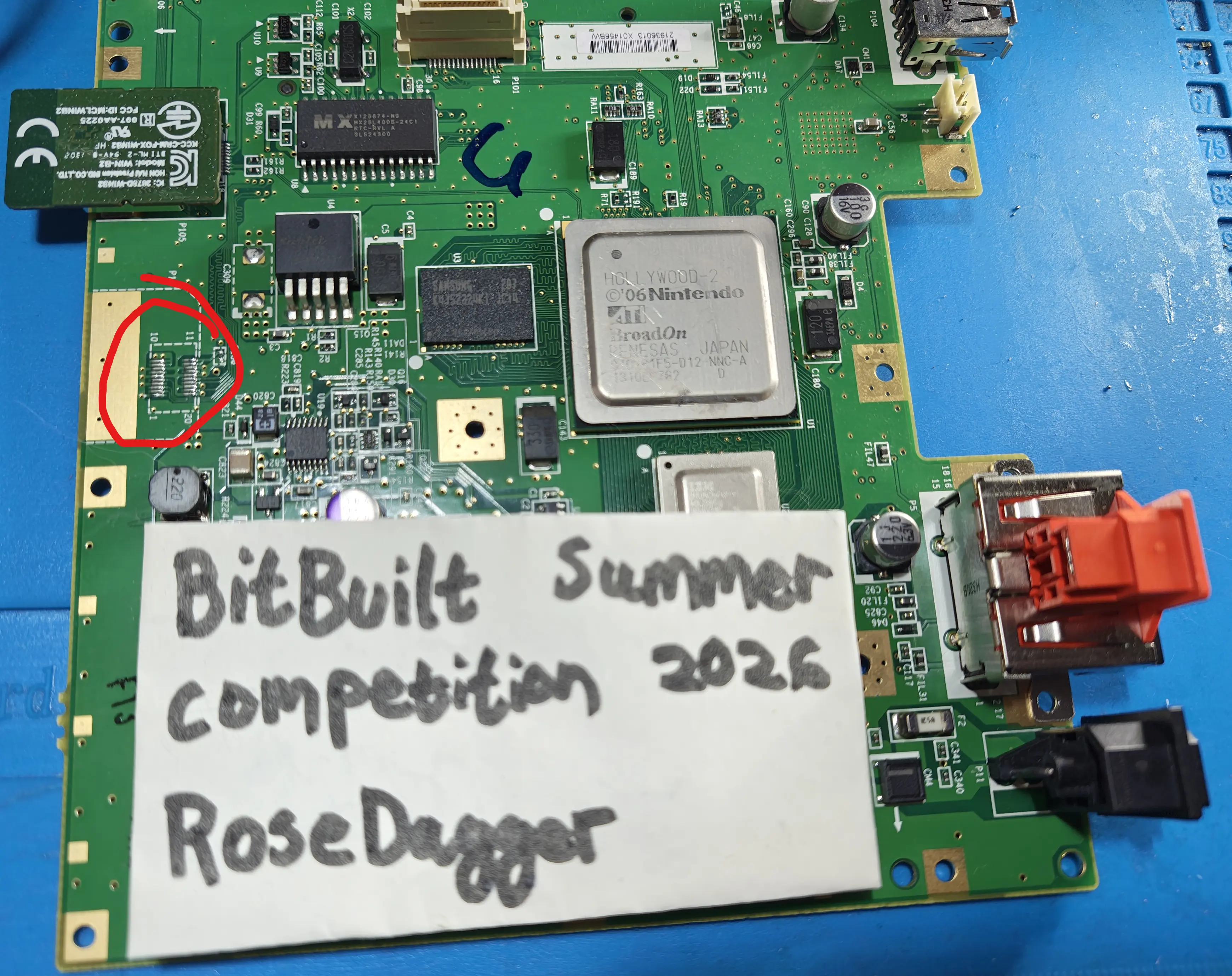
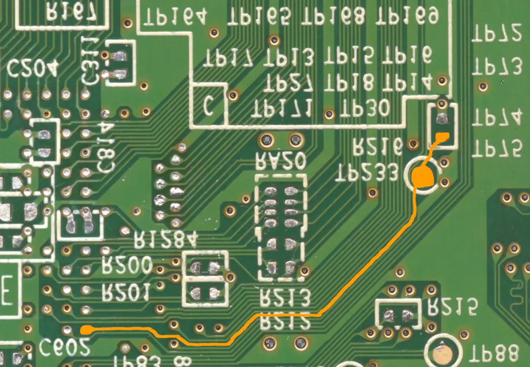
I check if there were any suggestions to others with this bug and see that the suggestion is to use the reset button to try and enter a sort of recovery or factory reset. But the Wii mini does not have a reset button… I check my spreadsheet for the reset button pin on the GPU, and check it on the Wii mini… The vias around that area is slightly different from the stock Wii, so I check the board scans for the Wii mini, and find the via, solder a button to it, and try anything I can think of… But nope, Delta is still bricked… For future reference the circled test pad is for the reset button.
Had I dumped the Delta NAND then I could have recovered, I could have written the original NAND image back, but since I had wanted to dump the NAND after installing RVLoader… And it bricked during the installation… I could not do that… So, I have a potentially broken HW2 GPU from Charlie, but working NAND, and a working HW2 from Delta with a broken NAND firmware, but since the GPU and NAND are keyed to each other, and I didn’t have those keys I could do nothing…
I ask in the discord, but no one has any suggestions beyond what I’ve already tried. So, I decide to give up on the second Wii mini. Maybe my WiFi solder job had been bad? And if I tried again, I would get it working? But I was tired and was still not sure if it was the WiFi as the other people with the “Exitting…” bug had been regular Wiis, so they should have had the WiFi card installed when they installed RVLoader. I decided to give up on Delta and just order another Wii mini (Echo), which was supposed to arrive the coming Friday, so it was only a week wait… Then thinking about my bad luck and how much time I had spent on just trying to harvest chips, I ordered another Wii mini (Foxtrot) which was supposed to arrive on Thursday.
2.4 Echo and Foxtrot, an encouraging chance to fix this mess
Well, Ebay lied, so they didn’t arrive till Tuesday the week after, and as I work over the summer, and don’t want to run the preheater while I’m away, I needed to wait till the weekend… So that was another 2 weeks wait… 6 weeks on waiting so far… I feel I’ve been here before with delay after delay…
The two Wii mini’s arrive Echo and Foxtrot, I jail break them, though bluebombing the second one took ages… Like over an hour… Think it only worked after restarting my PC to try over… So, if you are doing multiple consoles in a row, maybe try restarting your PC between each console to clear any issues? Or it was just my bad luck…
I dump the NAND this time from both Echo and Foxtrot. Then installed RVLoader, the default setting is that WiFi is patched out… I definitely patched WiFi in on Delta, a Wii mini which does not have WiFi… Anyway, the installation process goes well on both. So, I have two working Wii mini’s which are ready to be harvested. I pick one, Echo, as my third attempt, and wait till the weekend again… Though with luck on my side, I had booked a 2-week vacation to work on the PICO for the two weeks starting with that weekend, so it was just about perfect, I would have plenty of time to work on this, and to catch any bugs… Surely bug catching will be easy and no hassle…
Anyway, the weekend comes, and my vacation starts, and I echo the same steps as last time for Echo. I think I did 2 hours upside down, then 6 hours right side up, so 8 hours of baking. I harvest the GPU and CPU without issue from Echo. Delid them, without chipping the die, and check the resistances. See third time is the charm, I knew luck was on my side for once.
| 1.0V | 1.15V GPU | 1.8V | 3.3V | 1.15V CPU | |
| Charlie HW2 | 41 | 940 | 1.8k/6.6k | 154k | 41 |
| Echo HW2 | 26 | 1.7k | 822/1.5k | 1.8k/7k | ? |
| Rob HW1 | 139 | 19.7k | 71k | 16.5k | 42.7 |
Note 2: Some voltage rails change resistance between probes, latching high or latching low. So, I’ve listed both states.
3. The big quest for a tiny PICO
Before heading into the PICO, let’s have a look at the consoles used so far:
- Audacious Alpha – The first regular Wii, which is the one I cooked dead
- Brave Bravo – The second regular Wii, I tried to transplant the Charlie GPU into it, but got a RAM error, and abandoned it for greener pastures.
- Chipped Charlie – The first Wii mini, which I chipped the EEPROM of, and then put the GPU into Bravo to see if it worked or not.
- Disappointing Delta – The second Wii mini, which I bricked by patching WiFi in instead of out. And didn’t dump the NAND first.
- Encouraging Echo – Wii mini #3, successful harvest and delid without any visible issues. This is the one I’ll be using going forwards unless something tragic happens.
- Fixer Foxtrot – Wii mini #4, currently unmolested, and is being used as a reference for how a stock Wii mini works, how the clocks and signals are supposed to look, and help me fix the PICO.
3.1 Why the fuck did reballing get more difficult again?
So I have the HW2 from Echo, along with it’s CPU and NAND. I had ordered some fresh RAM from Aliexpress, so that I would not need to reball the RAM myself. So, all I needed to do was to reball the GPU and CPU, and place down the NAND, easy peasy right? I’ve already gotten a technique down for reballing the GPU and didn’t have much issues with it once I got it down. Sure, that was 3 weeks ago, and I’ve not tried again since, but surely, it’s not that hard, right?...
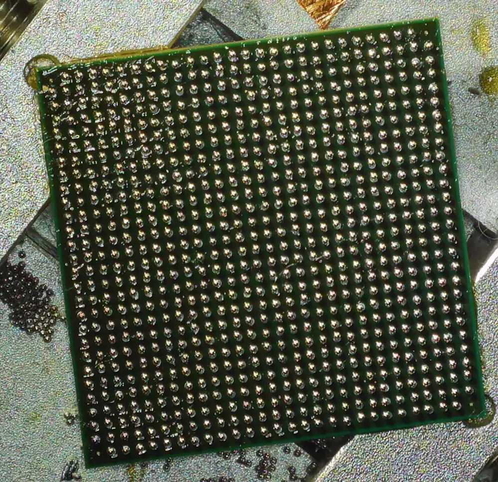
On my first few attempts on the Alpha GPU, I had not used enough flux, and it led to the balls not wicking down, and I burnt the GPU even more trying to get the balls to melt. As I preferred to not burn up my good Echo GPU, I decided to use more flux just to be sure. However… More flux means that the balls float more and want to clump together… So, I spent the next few hours heating the chip up, carefully watching for when the balls started clumping together, then immediately stopping, and separating them. Over time the flux would evaporate, and the balls would clump less and less, until I could finally reach the temperature needed to melt them and have them wick into place. I did it zone by zone and realized that the areas where the GPU was clamped into the jig was struggling to heat up, so I took the GPU out and rotated it so that I could heat those two corners.
Nicely placed down solder balls
Literal hell, each ball cluster must be separated manually. Why do I do this?
An eternity later, and it's a perfect reball...
Then over to the CPU… So, I had twice tried to get the stencil for the Wii CPU, however, even though both listings I tried said they had the Wii CPU in them, neither did… So, I ordered some generic stencils and found that the 0.4mm stencil fit, all I needed was to mask off all the excess holes. And as there’s no complex patterns on the CPU itself of where the balls should go, that turned out quite well.
Balls are placed.
Had to take the CPU out of the jig as it was soaking up all the heat, not letting any of the balls melt.
So now I had a reballed CPU and GPU HW2, all I needed was to plonk them onto the PICO, heat it up, and boom, I would have a working Wii, right?
I checked the resistance on the PICO first, just to be sure… and found that the 1.8V rail was shorted… I checked a few things, but I had my suspicions on the RAM. I had not used flux when I soldered it, as I had not realized how important it was to making the solder balls wick into place, and it had not had the same jiggle when I poked it. So, I removed it, cleaned up the area, checked the resistance, no short, fluxed up the area, and placed down a fresh RAM chip. It went into place a lot better, and I didn’t have any shorts anymore. However, the area under the RAM has started getting a bit scratched up from the solder braid...
With that fixed I moved back onto the CPU and GPU. I had prepped the area before hand with leaded solder, then removed it with solder braid so that there was only a thin coating on all of the pads and fluxed it up. Then I carefully placed the CPU and GPU down, aligned them, and placed the hot air nozzle above them. The nozzle was big enough that it would hit both at the same time, and honestly the entire board as well. I blasted hot air, while squinting in from the side to look at the GPU to see if I could see with my eyes if the GPU seated down. Then after a while I did my poke test… First poke, nope, not jiggling… Second poke, nada… Third poke, oh there it jiggled the way it does when the balls are melted, great. I just need to remove the heat and look at my amazing creation.
I don’t have an image unfortunately, so I drew how it looked. It seemed like my poke test had pushed the GPU back over a full row, and I had no clue at the time how the CPU ended up completely skewed… So, I immediately place the heat back on, removed the chips, and fixed all the components which had gotten moved back into place.
Hmmm, that went less amazing than I had wanted… But oh well, I’ll just try again! This time I’ll do just the CPU first, then get back to the GPU.
A few hours of babying the floating solder balls, and I had a CPU ready for attempt 2. I used plenty of flux on the PICO and used a smaller nozzle so I could better see what was happening. I heated it up, and suddenly the CPU starts moving randomly! The flux under it started boiling and gassing off, and it pushed the CPU around! That’s why it was all skewed last time! I try to correct, nudging it back into place, but the transplant felt dodgy at best… But not wanting to spend more hours reballing, I decided to move my microscope around to look in on the sides of the CPU, to see if the solder balls looked fine or not. I have good access to two sides, and bad access to the two others. And after careful analysis, I found what looked like a solder bridge on two of the data pins…
Well time for attempt 3. You know the drill, a few hours later and a lot of frustration, I was ready to try again. Last time I had way too much flux on the PICO, allowing it to literally boil and move the chip. So, this time I used a lot less. Then carefully lined the chip up, before moving my scope around to look in from the side. Now I don’t need to squint from the side to see if they melt, I can just look at my monitor to see when they melt. Brilliant, why didn’t I do that from the start? Right cause it’s a headache to move the microscope arm around and readjust it, and I didn’t think I needed it…
Anyway, I heat it up again, carefully watching that the alignment stays correct, and watching the feed from the microscope, and I can see when the balls start to melt, and how the chip settles straight down, no sideways movement! I don’t need to poke it to check!! I heat it for a while more, just to be sure the other sides and the middle are also fine. Then remove the heat and carefully analyse each side I can see from the microscope. Every side looks golden! Well seated down, good squish, no bridges, chip is square, and the resistance is good!!! I did it!!!!
Now the GPU… It’s way larger… I wait till the next day to get started on it, and it takes me the full day to reball it… It wasn’t that hard the other times I tried… I know I use too much flux, and I would save my sanity if I used less. But it felt safer, and I’m stubborn enough that I can handle doing a very annoying task for hours as long as I feel like I’m making some progress… Anyway, many, many, many hours later I’ve successfully reballed the GPU, now I just need to echo the same procedure I did with the CPU. A thin layer of flux on the PICO, place the GPU down square, change the microscope to look in from the side, then heat it up till I can see the balls melt on the microscope. And it went just as well as the CPU!!! Whoop!!!! I just need to analyse each of the sides.
Hmm the 3.3V buck boost is clearly not positioned well, it’s a micro-BGA component, but I have a replacement. And the NAND desoldered itself.
Hmm is that a damn solder bridge? How? It didn’t move! There were no bridges when I place it down… Damn it… But lets take a closer look just to be sure.
Hmm from an angle the bridge disappears and it looks more brown than metallic… It might just be flux… Let me check what pins that’s supposed to be… I know there’s a lot of ground in that area. It’s Ground and 1.15V… Let’s check resistances… Not a short! The resistance looks fine! Let’s check the other rails as well… They are also fine! Maybe I did it?!
I just need to fix the NAND and the 3.3V regulator and I can finally test the PICO. We are almost there! (Don’t look at how much is left in this work log…)
3.2 I HATE micro-BGA!
So, I used the same regulators as the ThunderKILL which used the same regulators as the ThunderVolt, which used a tiny micro-BGA buck boost for 3.3V. These micro-BGA components use balls that the size of a needle point, and the pad’s are not any larger… I had one unused backup of this regulator, so I heated it up to remove it… The regulator would not budge… I keep waiting for it to heat up enough… But the point never comes… I up the heat on my hot air, and finally it want’s to come free. So, the solder balls they use are apparently very high heat… I clean up the pads and put some flux down, then place the regulator down and start heating it. The silk screen outline around the chip is taller than the balls, so I can’t really look in from the side, though I probably should have tried. I heat for a good long while, at a higher temperature than normal, just to be sure the high heat solder balls will melt, and I don’t poke it. Once it felt like enough, I let it cool down, then poked it to see if it would stay or if it would come loose. And it stayed in place, so some of the balls stuck down at least.
I connect up the wires for the ATTiny, so that I can flash the firmware to it, and do some modifications to make the ThunderVolt firmware fit the picothunder (I used some different pins and components, and moved the LED, the Thundervolt has a dimming LED, I don’t as I didn’t realize the LED pin mattered, or that that was a feature). Once that’s done, I connect the test dock I made and give it power.
The plastic bits are there to make the PICO thicker so it will press into the contacts properly.
On the Thundervolt, the LED will breathe when everything is fine, and it will flash an SOS if it fails somewhere. My version will blink regularly if everything is fine or do the same SOS if something wrong. I check the LED, and it’s blinking steadily. Great! Awesome! This is really coming together! Let me just check the voltages to be sure. 1V? Yes! 1.15V? Yep! 1.8V? Right on! 3.3V? Hmmm… why am I getting 0V on 3.3V? That’s not great… Let me check the code again. Hmmm it will SOS if it can’t find and can’t talk to the regulators. But it never checks the voltages, or what the regulators has to say. So, the 3.3V reg is present, is answering I2C, but is not converting… Hmm, let’s look at the datasheet for that regulator, let’s see what status registers it has, I’ve use different regulators before which had a lot of telemetry and status I could access. Hmmmmmmmmmmmmm… It only has Power Good, and Temperature Good… Let’s check those… Okey it’s reporting Power Not Good… Great it is aware it is not working, but won’t tell me why…
I double check that the inductor I have has the correct ratings and that I didn’t mess up the size of it. The datasheet, and the ThunderVolt Schematic says 0.47uH, checking Digikey, the inductor I ordered was a 0.47uH inductor. So, it seems fine. I keep checking some more stuff, but it feels like it mostly comes down to the regulator, which has those cursed micro-BGA pads, and maybe it’s not fully seated, or something is wrong with the inductor… The inductor is easier to replace so I do so. I add a bit of fresh solder paste just to be sure it will stick down, the solder which is there currently has been heated and cooled a good few times now. I heat it up… And the solder paste starts spreading around as it becomes more liquidy… And some of it goes under the regulator… Just absolutely perfect, that’s exactly what I wanted… Fresh solder getting stuck under the micro-BGA regulator that I don’t have any spares for… I check just to be sure… And the switching pins and vout are shorted…
So, I desolder it… clean up the solder… then try to reball it using the solder I have. I tin the pads on the regulator and on the PICO and try to get them to merge. SOS the Tiny can’t talk to the regulator… Off with it again… Only tin the chip and not the PICO… Hey it’s talking again, and I’m getting some voltage on the 3.3V rail! 0.5V is some voltage… but not the right voltage… I’ve been probing the everything with my oscilloscope, both before I had to replace the regulator again, and after, and it never properly converts. On the 0.5V it tries to convert for a little bit, then gives up… And so do I…
This 3.3V micro-BGA regulator is the bane of my life, I just wanted to see if the PICO would work, why does it hate me so much? Fine, I’ll just get rid of it, and replace it with an external regulator, I have a few of those laying around. And I swear for the future to never using micro-BGA for any projects I need to solder myself ever again!
I change the firmware to not look for the 3.3V regulator, then I try one regulator I have. Out of circuit I adjust it to 3.3V, then solder it in… The 3.3V rail is only supposed to draw about 0.25A, so it’s not massive, surely it can handle it… Nope… I don’t get the voltage I need… Fine I have another slightly better regulator that I’ve use before which should work. I solder it in, adjust it, aaaaaaaand 3.3V!!!!! I check the other rails, AND…. They are still good!!!!!! It’s alive!!!!!! Mwahahahaha!
3.3 Pico Debugging
With all the power rails operating, I just need to attach the video out to the dock, and check my monitor, surely it will be that simple right?... No image… Fine let’s check some stuff. The CPU and GPU both heats up when connected to power, so they are doing something. The debug port is outputting 0x80… It’s a solid 3.3V and that’s not a valid code… Okey let’s check the video out pins, which feeds into the AVE. The 54MHz clock should be reliable, that’s reading 27MHz…. Hmmm that’s not right… Let’s check the data pins? No activity… U10? Hmm the only place I have access is a tiny via right next to the NMOS. So I carefully scratch the solder mask off and probe it. Oh, this is not correct, it’s going high while the 3.3V regulator is still booting, maybe the external regulator is taking more time than the intended regulator. But that is an easy fix, just need to change the firmware of the Tiny to extend the delay.
Hmm I’m seeing the same behaviour… Let’s delay it further… Nope… a 2 second delay? That’s something I should notice, is there a 2 second delay from plugging in power, till the signal is captured? Nope it’s instant! I check the LED, that gets delayed from blinking by 2 seconds, so the Tiny can keep time… Maybe the NMOS isn’t soldered properly? It’s another very tiny component with very tiny pads… And sure enough, the gate and source pins were not wetted… Okey let’s resolder it… And probe it…
Oh, it turns on initially, then turns off as the Tiny wakes up, then turns on again after the delay. The 3.3V regulator is not connected to the enable line for the other regulators, so it just boots as soon as it gets power. But at least the delayed U10 reset is happening now, after the rails has fully powered up.
Checking the 54MHz video clock… Still 27MHz… Okey on to the next issue. Let’s check the clocks around the board, first checking the stock Wii, aka Foxtrot. Okey the main clock is supposed to be a 27MHz sine wave centered around 1.8V. The CPU clock is a 243MHz sine. Let’s check the PICO. The main oscillator is… Flatlining… That’s not good…
I try to reflow the area. Nope. I try to replace the load caps assuming there is less stray capacitance than I did for my first calculations. Nah. Hmm, the probes have have a 1x and 10x switch, 10x is for more sensitive and small signals, but I’ve never really used it, and didn’t need it for the stock Wii, but I replaced the crystal with a smaller one… Let’s see what happens if I change mode… Oh there is the sine wave, 27MHz just as expected.
Okey according to this, the CPU is supposed to be 243MHz and the RAM is supposed to be 486MHz
Let's check CPU clock... 237MHz! Great, close enough! The GPU and it’s clocking and PLL systems are working! And the CPU gets an appropriate clock.
Now let’s check the RAM, most of the traces are hidden under it and under the GPU, but I have access to the terminating resistors for the clock, which is supposed to be 486MHz. And I measure… Garbage… centred around 1.8V
Well that’s not what I want to see… Let’s check to stock Wii… Hmm I’m seeing something there, but it’s not very clear… What’s going on? It’s centred around 1.3V…
Why is the signal on the stock Wii so weird? Hmmmmmmmmm…. My Rigol DHO914s oscilloscope is rated for 125MHz… the DHO924s is rated for 250MHz, and uses the same hardware, just a different firmware… Those who are good at math might have notice an issue… 486MHz is slightly larger than the 125MHz or even the 250MHz that my scope is rated for… XP Though I could at least see something of the waveform for the 486MHz on the stock, even if it was very distorted. The PICO is not even showing that…
I checked the Vref for the RAM, which is supposed to be 70% of VDD, which it was, for both the vrefs.
Also checked there is no activity on the datapins for the RAM.
I'm not sure what else I can poke to investigate...
Next step might be to desolder the RAM again? It was hanging upside down while I was soldering the GPU so it might have started to desolder itself? Though it looks fine from the outside...
There is also the risk that the scratched solder-mask under the RAM is causing issues and something got bridged? Though then I either need to get lucky when I solder a new chip on that it does not short... Or start over on a new board... Which would be hell, I don't have a lot of backup components, so I would have to order more, or harvest from the current board...
Or me moving the DQ groups around messed it up so much it wont initialize? Or the interference from the compact traces makes it give up and not not initialize? But I would expect the 0xF1 boot code if the GPU came alive enough to test the RAM and it failed. So it fails before even reaching Boot0...
Maybe the RAM is a red herring and it's showing no activity as the GPU has not tried to initialize it? But then what else might be wrong to the point the GPU does not even reach Boot0? And never tried to initalize the RAM or start the RAM clock?
And that's about where I am. Unsure of what is wrong or why. And mostly poking and prodding stuff to see what behaves as expected and what does not.
4. Postamble jabber: The reality check I want to ignore
So, when I started this project, I set out a few goals and made a rough gantt chart/timeline to see how much time I would have for each step. I had planned to update that chart as I went, but of course I kept forgetting about it. But now, with two months left, and having lost one and a half months to trying to get an HW2 GPU I could use, it might be time to return to that overall plan.
As Loopj said in the discord:
Which is true, but at least for me, it gives me a visual indicator of how much time I have left and what is left to do in that time, so I made another one, updated to how things actually went.
As you can see, I failed to deliver on most of those shaky promises, and the full month buffer I had made is completely gone. There might still be a small chance that **IF** I get the PICO working in the next week or so, I **MIGHT** be able to finish, as long as I don’t need to do any reprints or revisions… Something that I failed to accomplish last year…
Of the original goals I had I’m going to have to cut down on some of it to have any chance. Mainly the TV Dock. I don’t have the time or motivation for it. It was supposed to be my shot at the smallest Wii ever made, smaller than the Kawaii, but I had no ambitions or wants for it beyond trying to claim that title, so it’s best to just… not do it. I’m also not gonna mess with MIPI and just stick to the HDMI driver board which came with the display I got.
So, my current goals look like this:
Main goals:
- Fully redesigned Wii motherboard with transplanted CPU, GPU, RAM and NAND. (mostly complete/in debugging)
- Putting the redesigned Wii into a GBA cart. (mostly complete, waiting on the PICO to work before I do a final pass on it and order)
Create a simple dock to test that the redesign worked.(Killed and abandoned, maybe the test dock counts?)- Create a handheld dock in the shape of a GBA. (In progress, waiting on the PICO before committing more)
Create a TV dock, which should hopefully be the smallest Wii ever made (so far).(Still nope)- Actually, having something work at competition end for once. XP (Let’s see, it would be nice, but the chances are diminishing)
- GBAWii4: MX, GCVideo, MelonHD,
MIPI display and redesigned driver board, use the included HDMI driver board like a sensible person. (In progress, waiting on the PICO, except for a redesigned MIPI driver board, that’s dead.) TV Dock: MX, Bluetooth, AVE/component out, sensor bar plug, 4 GC controller ports.(Nah)
Anyway, think that’s enough for this update, I’ll try to not wait as long on the next one, and make it slightly shorter than this monster update I just really, really, really wanted to get to the promise of last time, either have a working PICO or debugging it... I won’t make such a promise again. But let’s check Word just for fun, without images I’m at 15 pages, ~7500 words. If you read all of this, congrats and thank you, I spent way too long writing this XP Time I probably should have spent on debugging…
Attachments

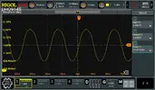
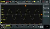


Oh mah lawd

Amazing work so far, working with BGA sucks. I wish you the best of luck--don't work yourself too hard!
- Joined
- Jan 15, 2021
- Messages
- 68
- Likes
- 267
- Portables
- Wii PICO (Complete), Wii Zero (WIP), GBAWii4 (WIP), GB Adwiince v3 Revenge (On Hold), GB Adwiince v2 (Dead)
I got a bit busy so I’m going to split this update into two: (Don't worry it's not nearly as long as the last one, only 1700 words)
Part one: August 15th
Heya time for an update, and it’s a big one!
First off, I found out what was the issue last time, it turned out to be the NAND which was not properly soldered. I tried a few different things, including removing the CPU and checking all the pins, then removing the RAM, fixing the damaged solder mask underneath it, and checking everything there. Eventually I resoldered the NAND and... boom!
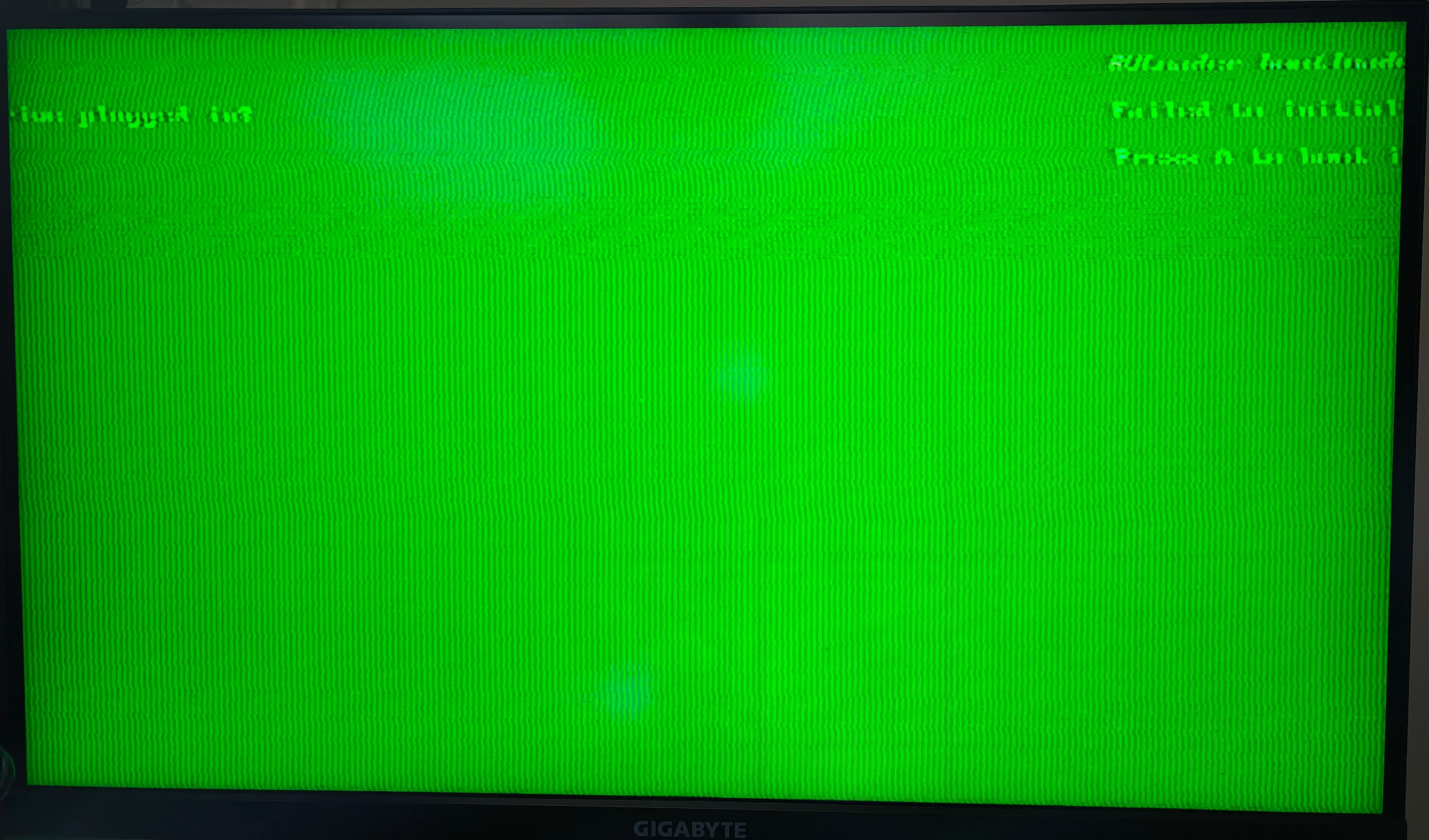
Now, that might not be the greatest image ever, but it’s an image! And you can see some of the details you expect from a Wii booting. Including how RVL is complaining about missing the USB drive. Now this image was a pain to get, the image would not sync properly, and I would lose the signal often, and touching the pins on the connector would change how the signal appeared, and how it behaved. With the connector being the main suspect, I tried touching up all the pins with my iron, and Tada!
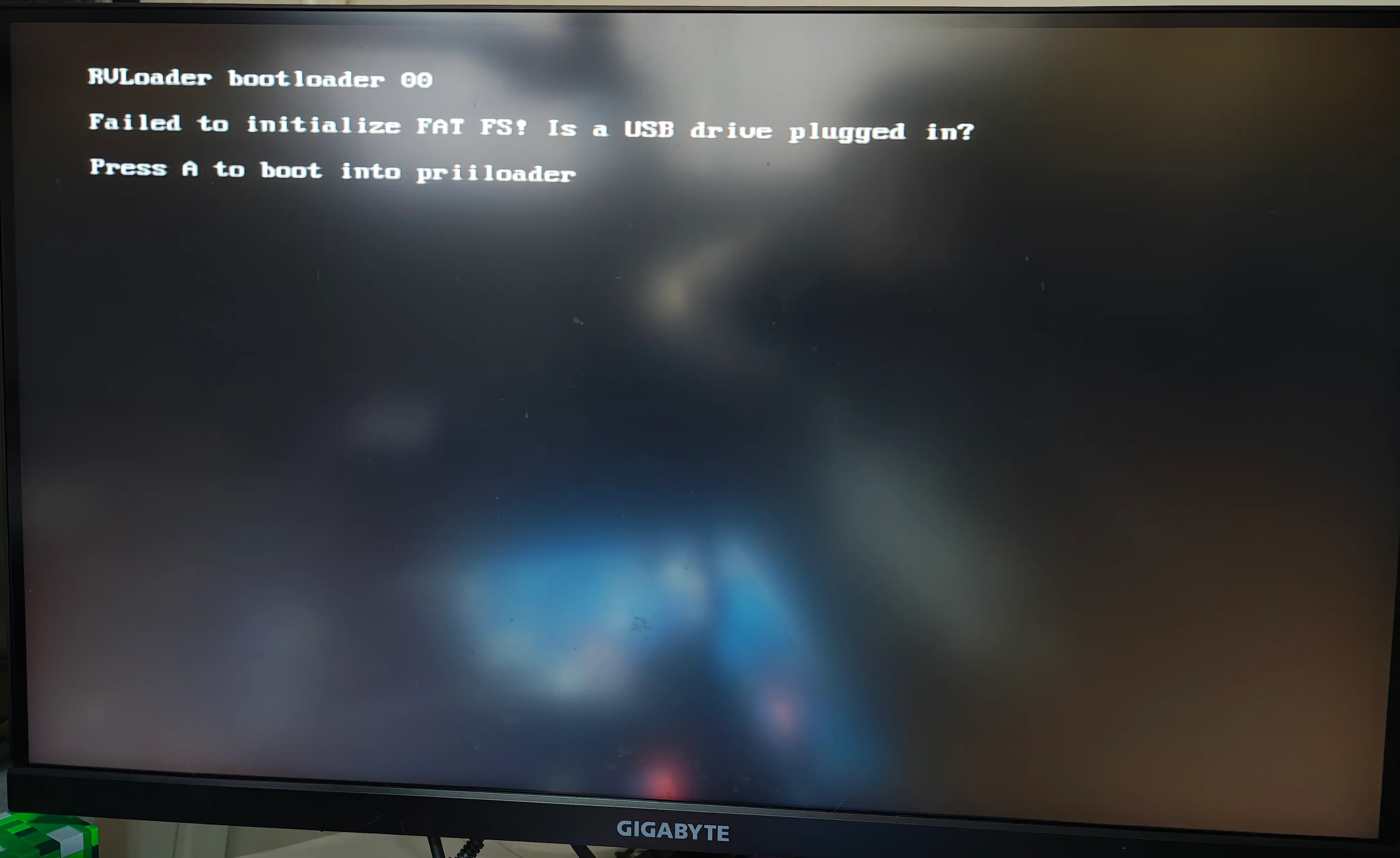
Next, I just need to plug in the USB and we are good to go right?... Nope, it is not reading the USB drive… I check that I didn’t mess up D+ and D- or something else silly. But no, they seem fine. I check with an oscilloscope to see what’s happening, and it seems like I’m not getting a proper connection…
I’ve had a lot of connection problems between the PICO and the Dock… I wanted the PICO to be as small as possible, while using the normal GBA connector. However, the GBA connector assumes a much longer wiping/insertion distance than I’ve given the PICO, meaning that the contacts only connect at the very edge of the PICO, and any misalignment would make one side not fully connect…
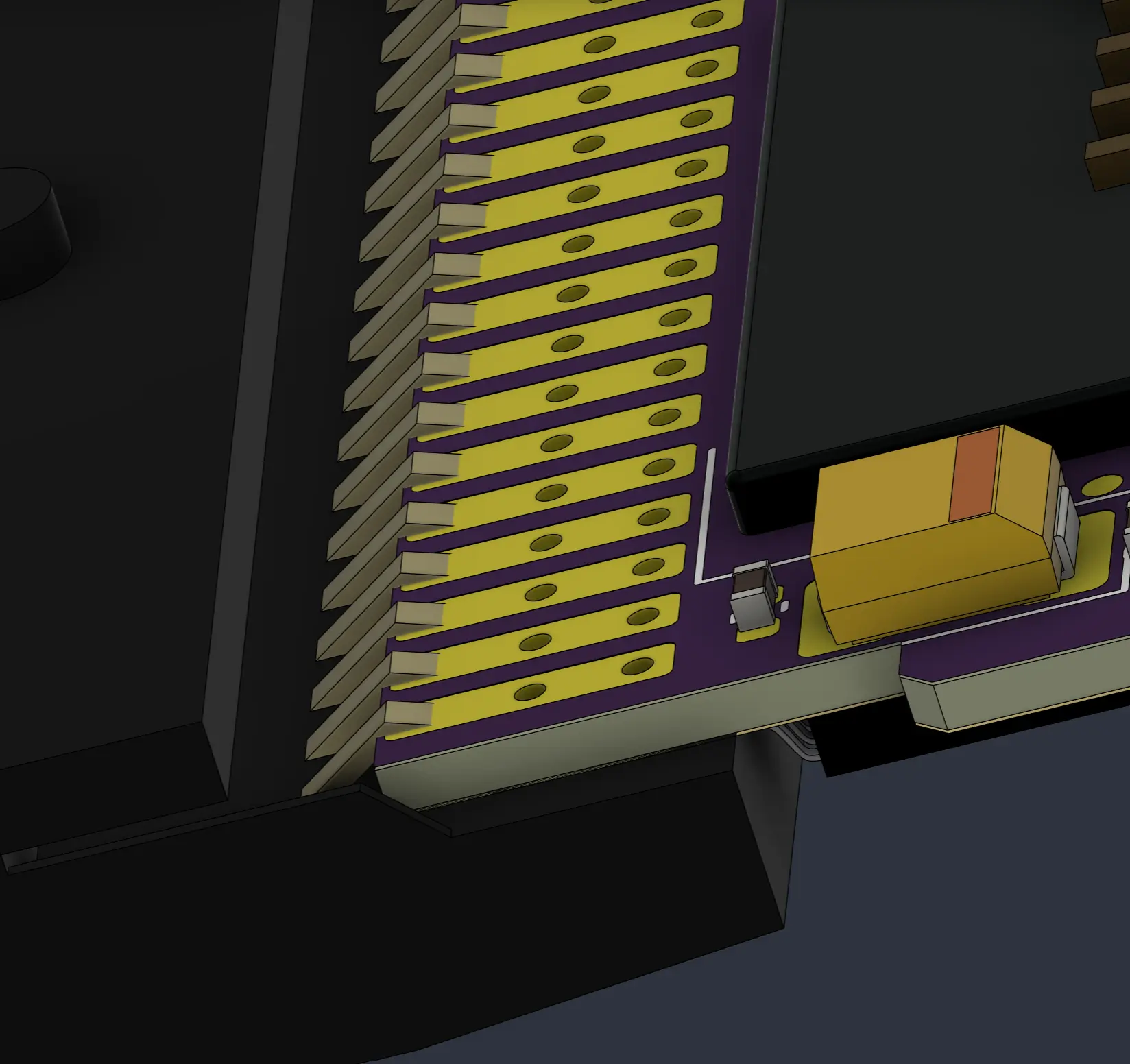
After fiddling with it for a bit, I managed to align it perfectly and insert it at the perfect distance so that the pins made contact, and the USB could be read. Though this connector design is not great for what I need…
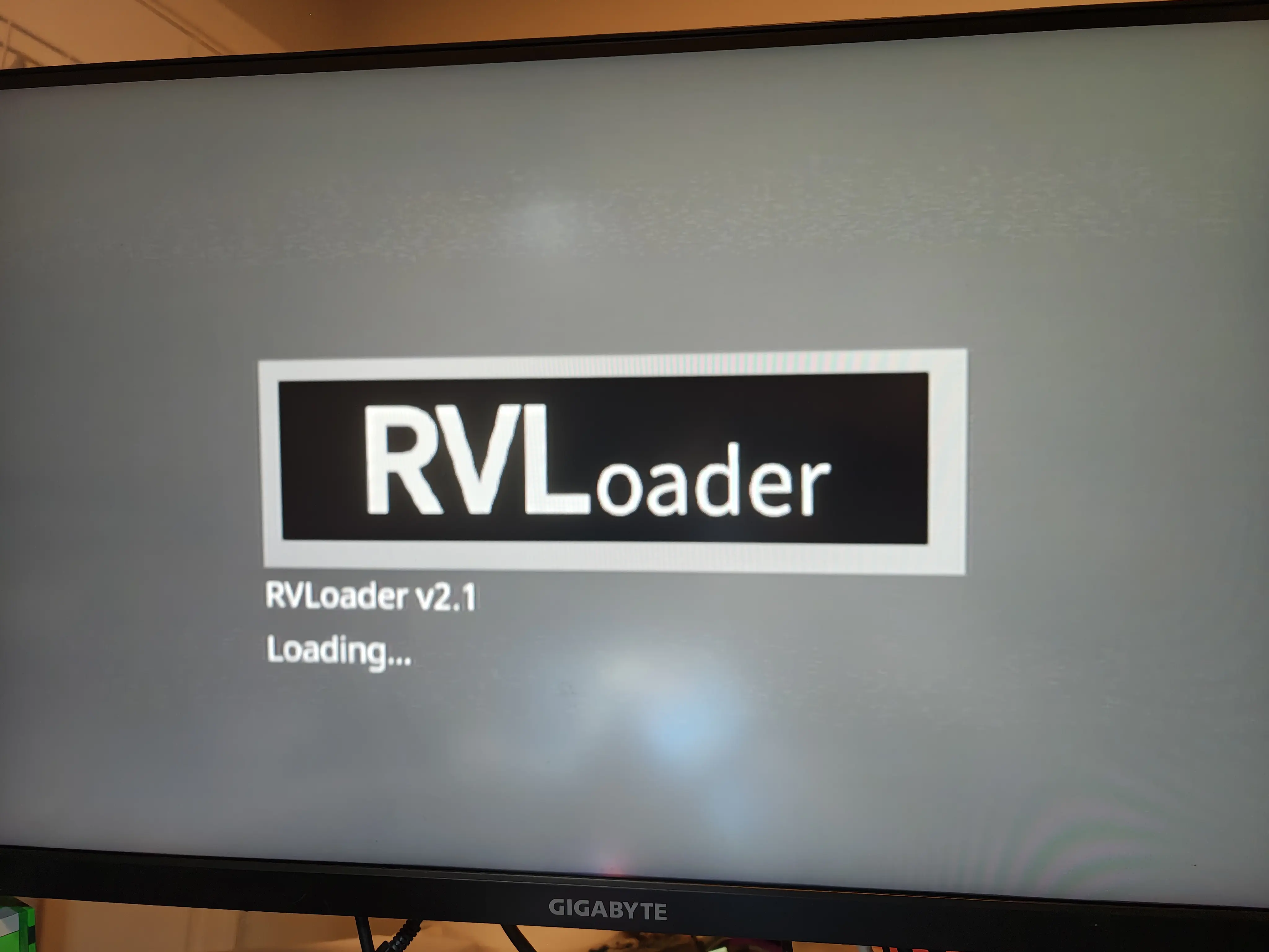
But it works! It fucking works!! Hallelujah!!!
Now let’s see if it can play anything. Starting with Super Mario Sunshine.
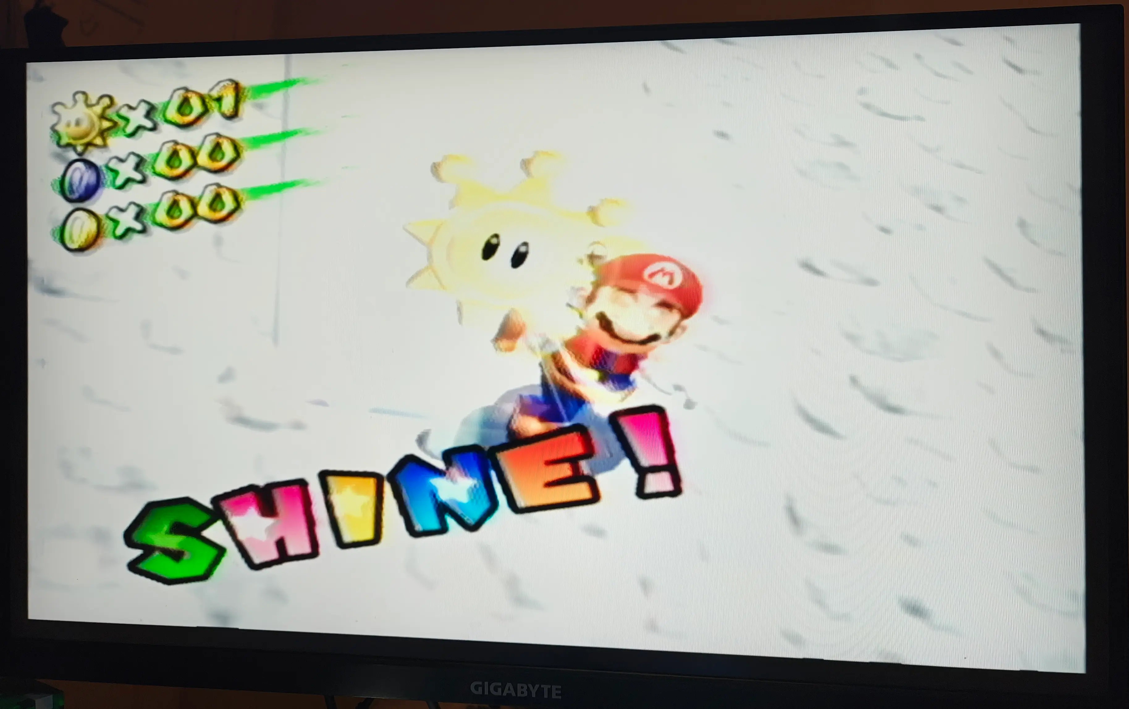
It runs! It works!! It can actually play games!!!
Now let’s see if it can play a Wii game, let’s try Mario Kart, as it has native GameCube controller support.
I played two cups back-to-back without any issues or instability!
I fucking did it! I have a working Wii on a PCB which is only 52x34mm! I moved the RAM to the backside and changed the DQ groups around and it fucking worked! I moved the CPU closer to the GPU and squeezed the traces together and the cross coupling didn’t kill it! The passives were moved around, and large sections are blocked off by the RAM and NAND so I could not place the passives optimally where they should go, but it still worked! It’s kinda insane that it actually worked with everything I changed at once XP
So I’m gonna call this conservatively a massive success as a prototype!!
Glory pics!
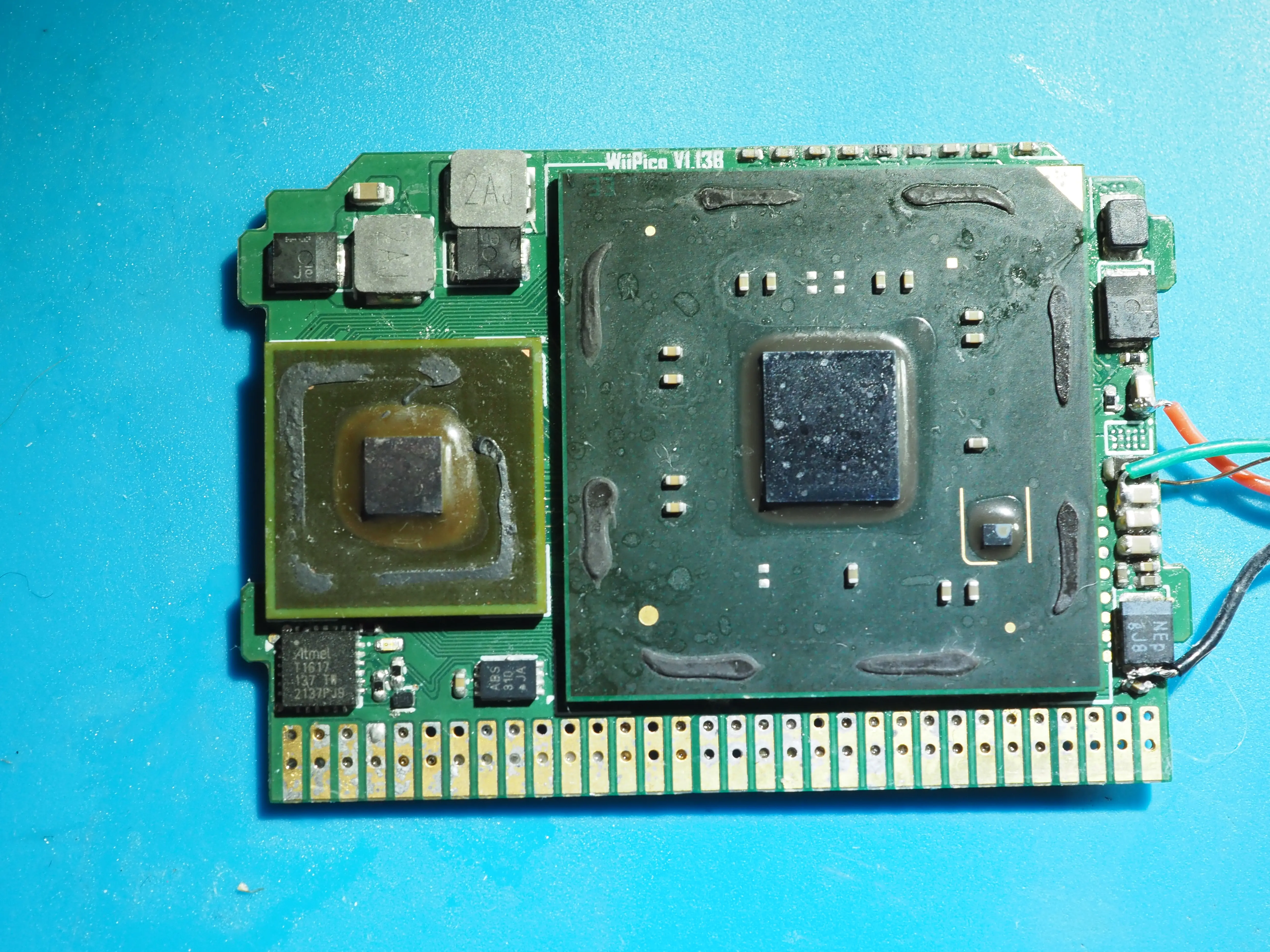
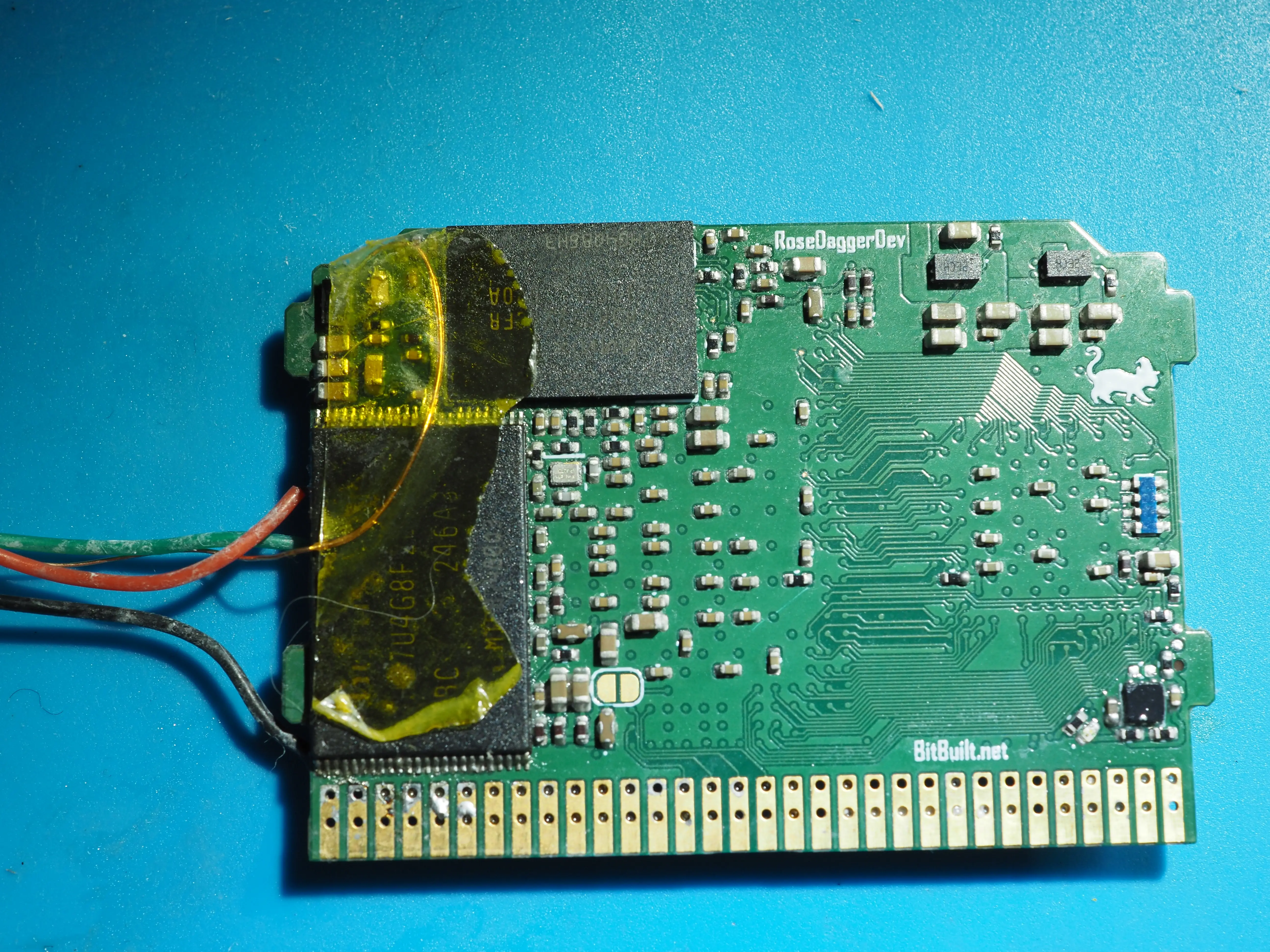
The testing setup:
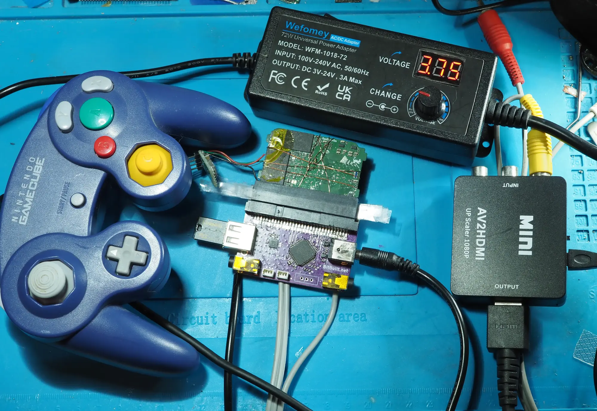
Yes I ended up holding the heatsinks down with magnet wire and thermal pads
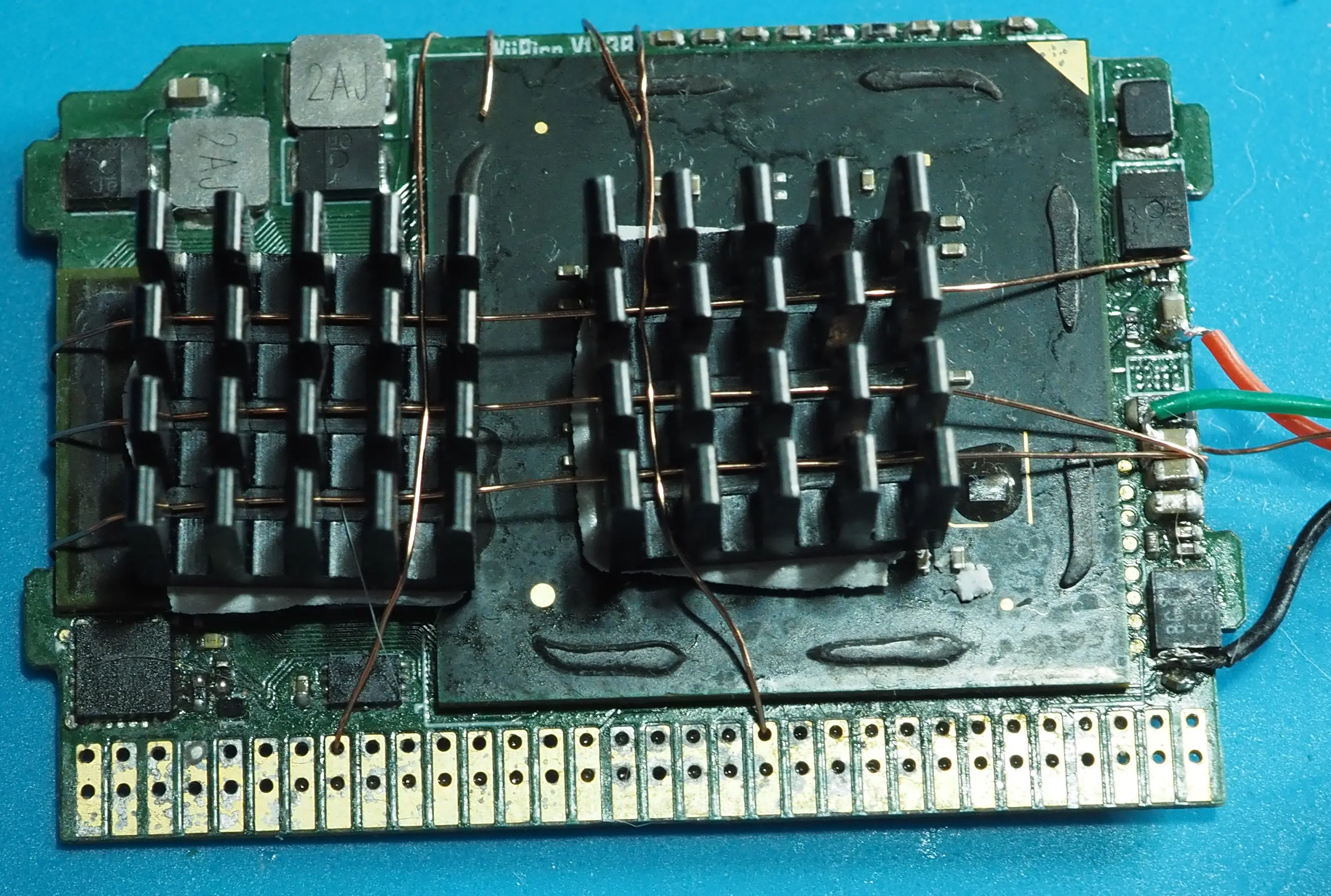
The Pico in the dock, with the 3.3 external regulator on the side. And plastic shims under the connector to give it enough force to mate properly.
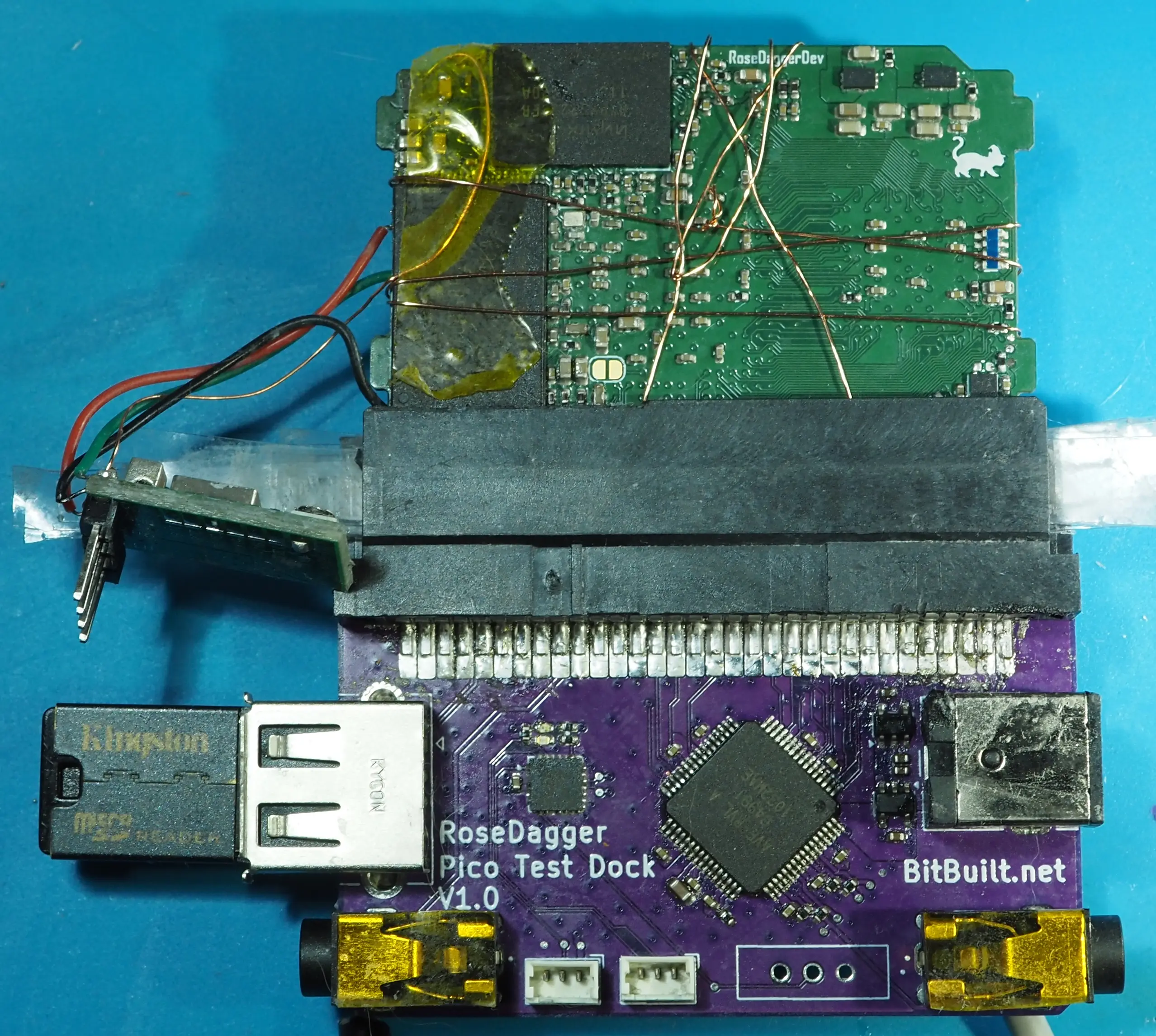
I had planned to make the Video out and GC out into mini jacks, but then I forgot to order solder-able mini-jacks, so I just soldered directly on the terminals.
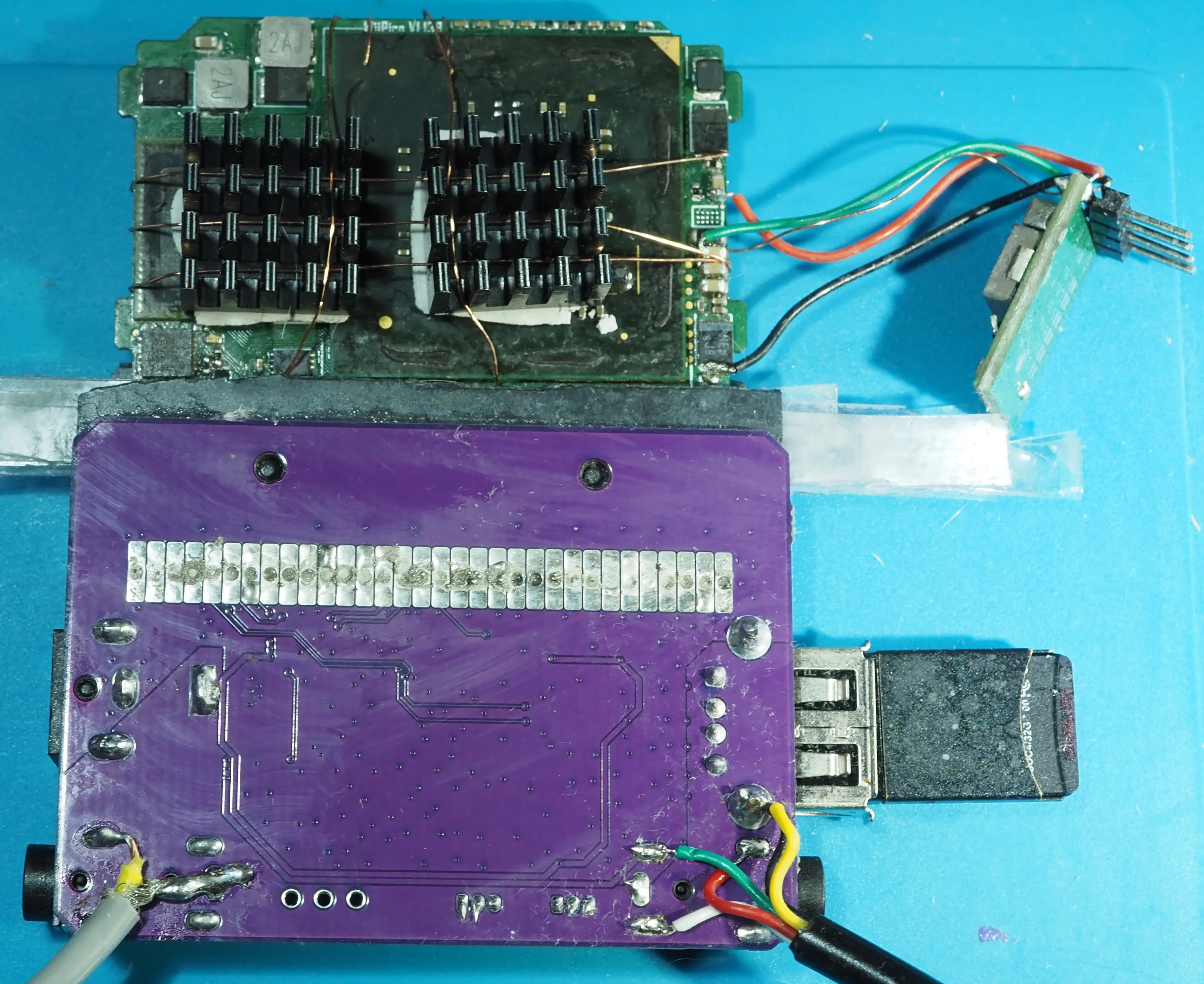
I had a handheld fan running over the setup to ensure it was cool enough to run.
Though there are some issues that I want to deal with for a second revision:
Part two August 31st
With the success of the Pico prototype, I needed to kick my arse into gear. I had only a month and a half, to pull this off, on top of doing work. So, I down prioritized getting the update above out, which is why it comes half a month late XP
Now, however as I’m still busy, I’m gonna lightning round this:
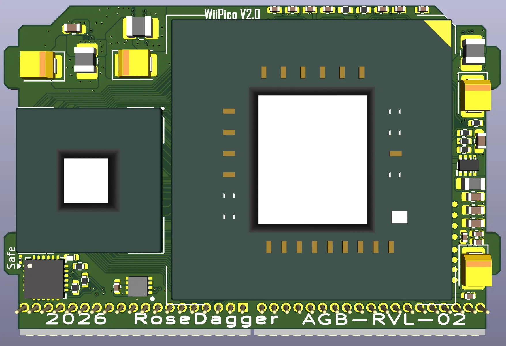
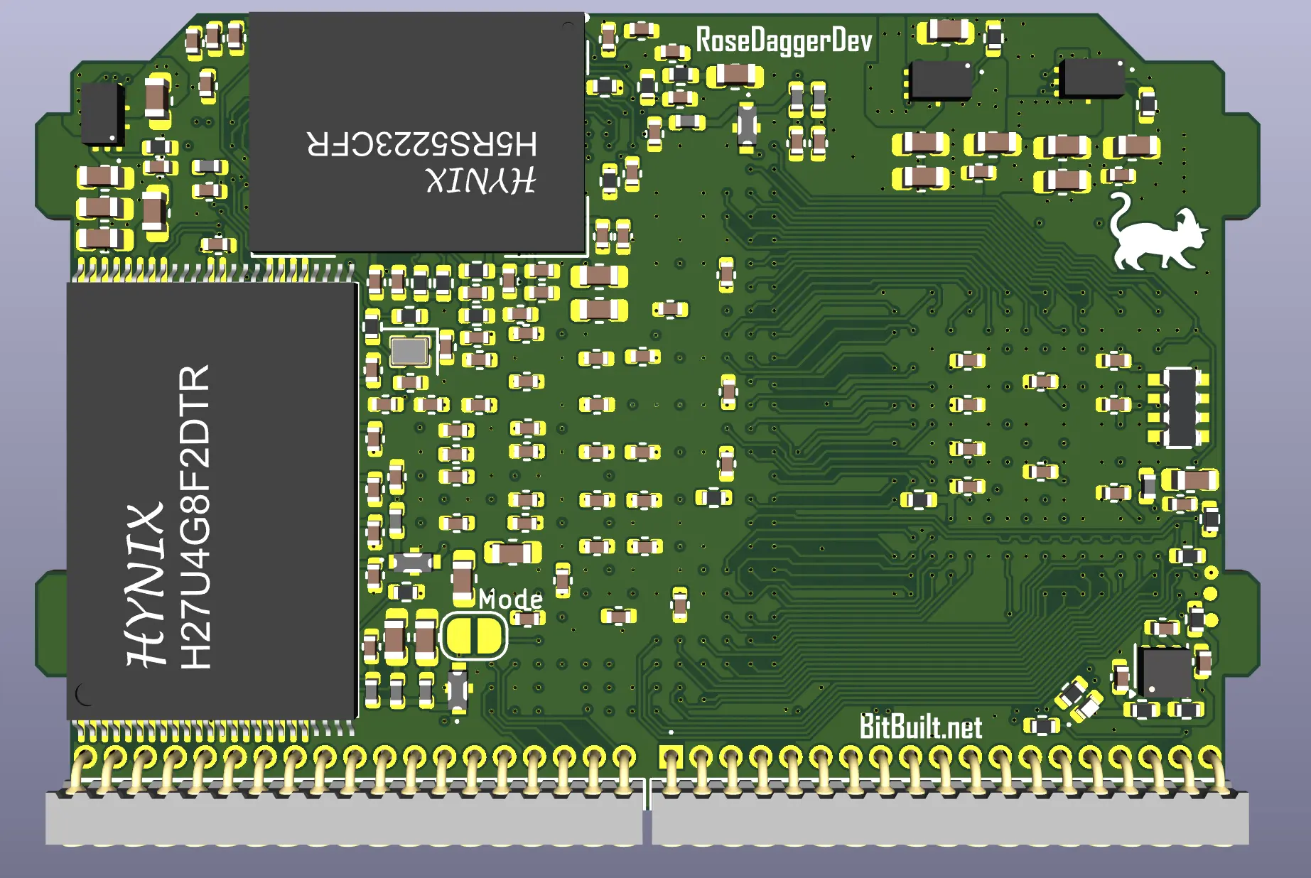
I got a tip from YveltalGriffin to use a tiny non-I2C buck-boost he knew about and used that to replace the DSBGA and then use the DAC on the Tiny to adjust the feedback node. I had used that trick before on a different project, but didn’t think to use it here, and would have overlooked the absolutely tiny regulator he found. So, all praise to him for saving me from DSBGA hell XP
Also Pogo pins and targets are expensive as hell… I’ll not use them again if I can avoid them... Damn I really hope they work as I intend…
However, the Pico wasn’t the main work, I just wanted a minor revision on it to fix some issues and the connector. The dock or GBAWii4 was the main issue. I had a mock-up of it, the shape of the PCB was done, and most of the main components were added to the schematic. But I needed to go over it to fix any missing components and validate it. And then lay it all out and trace it. And I had a deadline… I ended my internship Friday last week. Uni starts up Tuesday next week. I have one week where I’m not in my final year in uni or working, so I got to make the most of it. Which meant that I needed to get the dock ready as quickly as possible.
And with a lot of blood, sweat, and exhaustion, I did it! Here is the GBAWii4 dock!
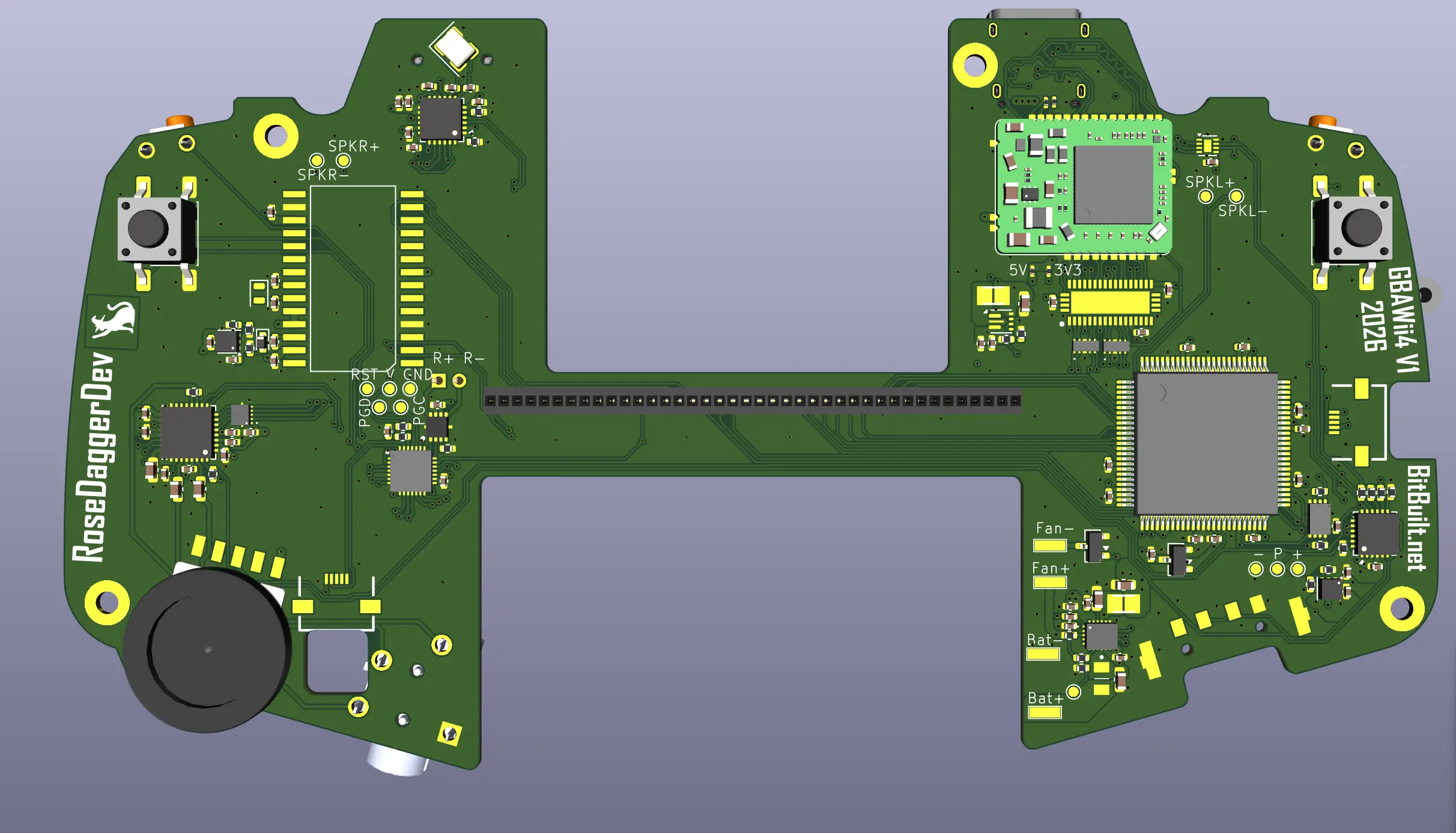
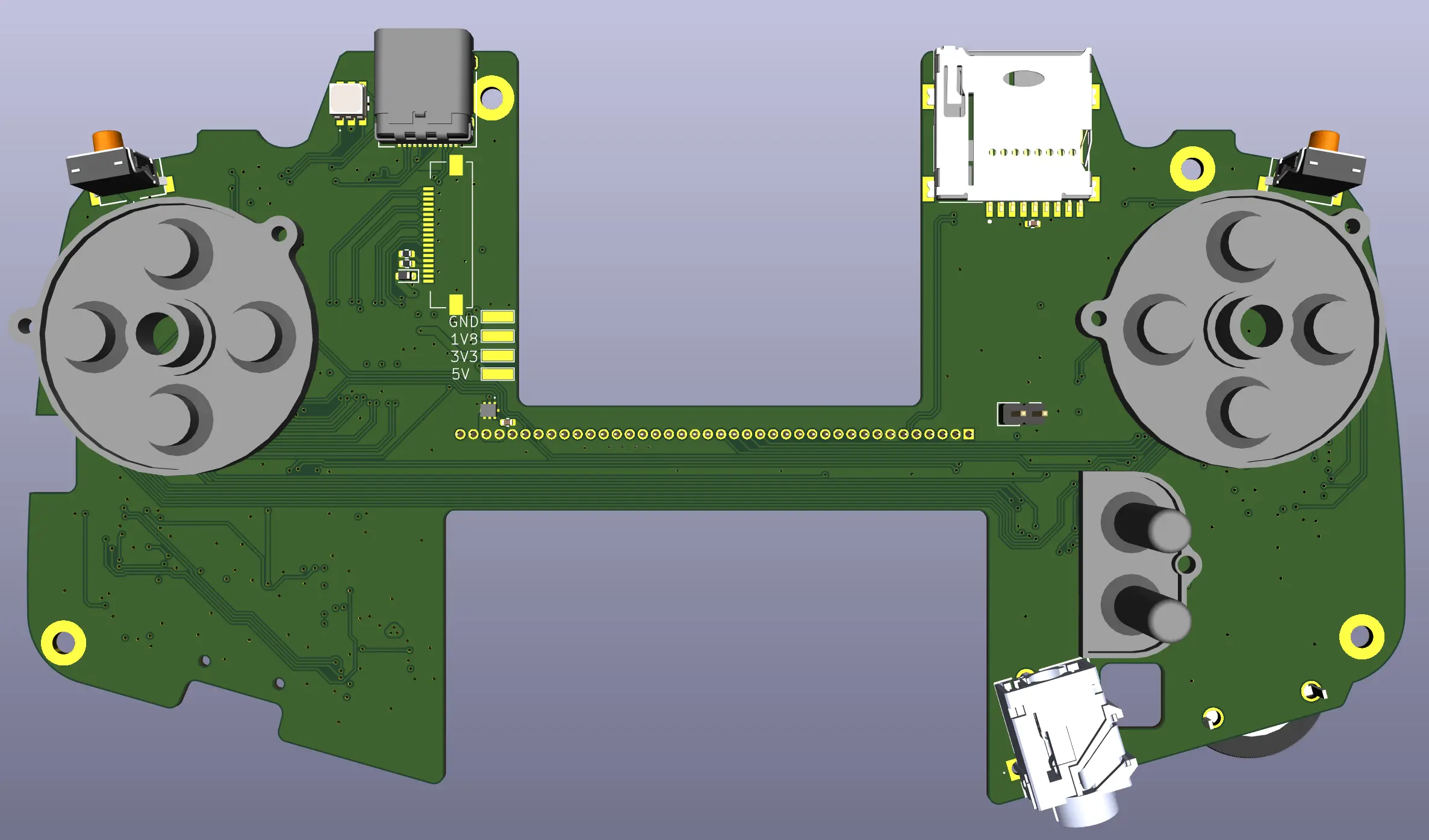
And inside the GBA shell: Yes the bottom cutout was for some larger fans and I didn't bother resizing the PCB after changing the fans.
And the copper looking thing on the bottom is the flex PCB from the display and display board.
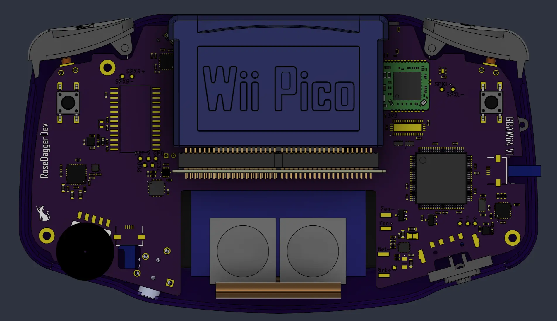
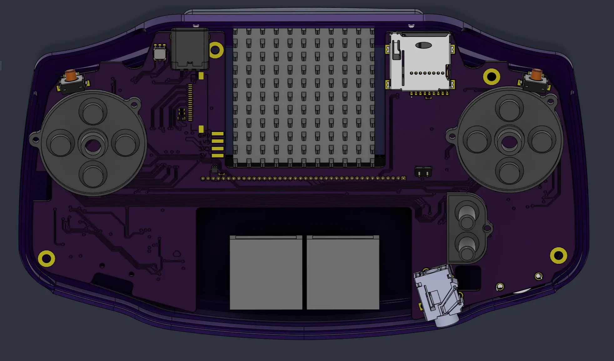
With batteries:
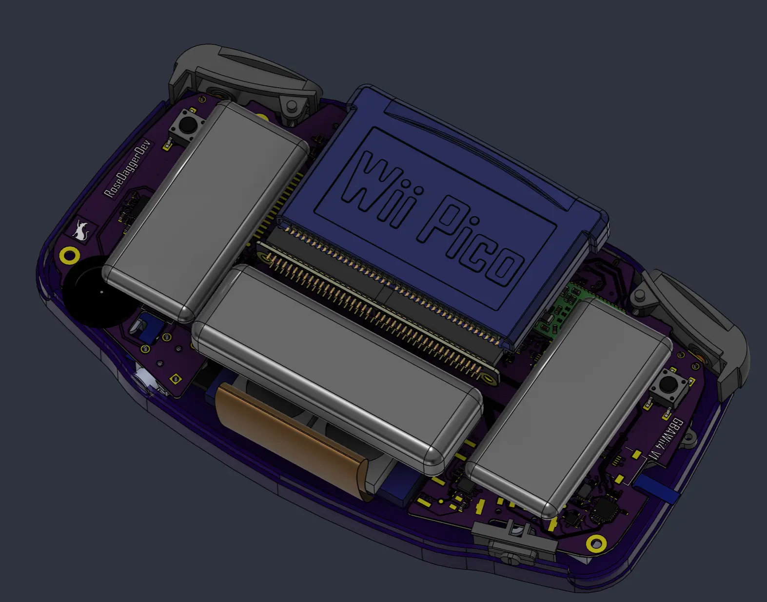
There is a small riser for the pogo pins, I needed to lift them up. But it will also allow me to mount the pogo pins to the back shell where the cart sits and then connect it into the GBAWii4 PCB with the regular connector.
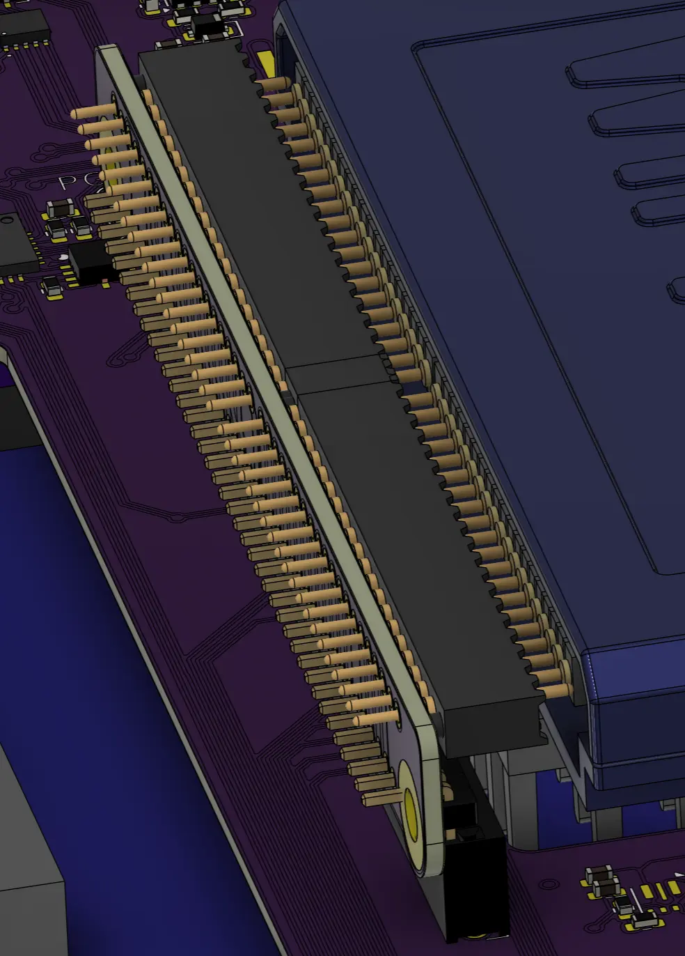
The routing could have been neater, I didn’t have much time to refine it or go over it again.
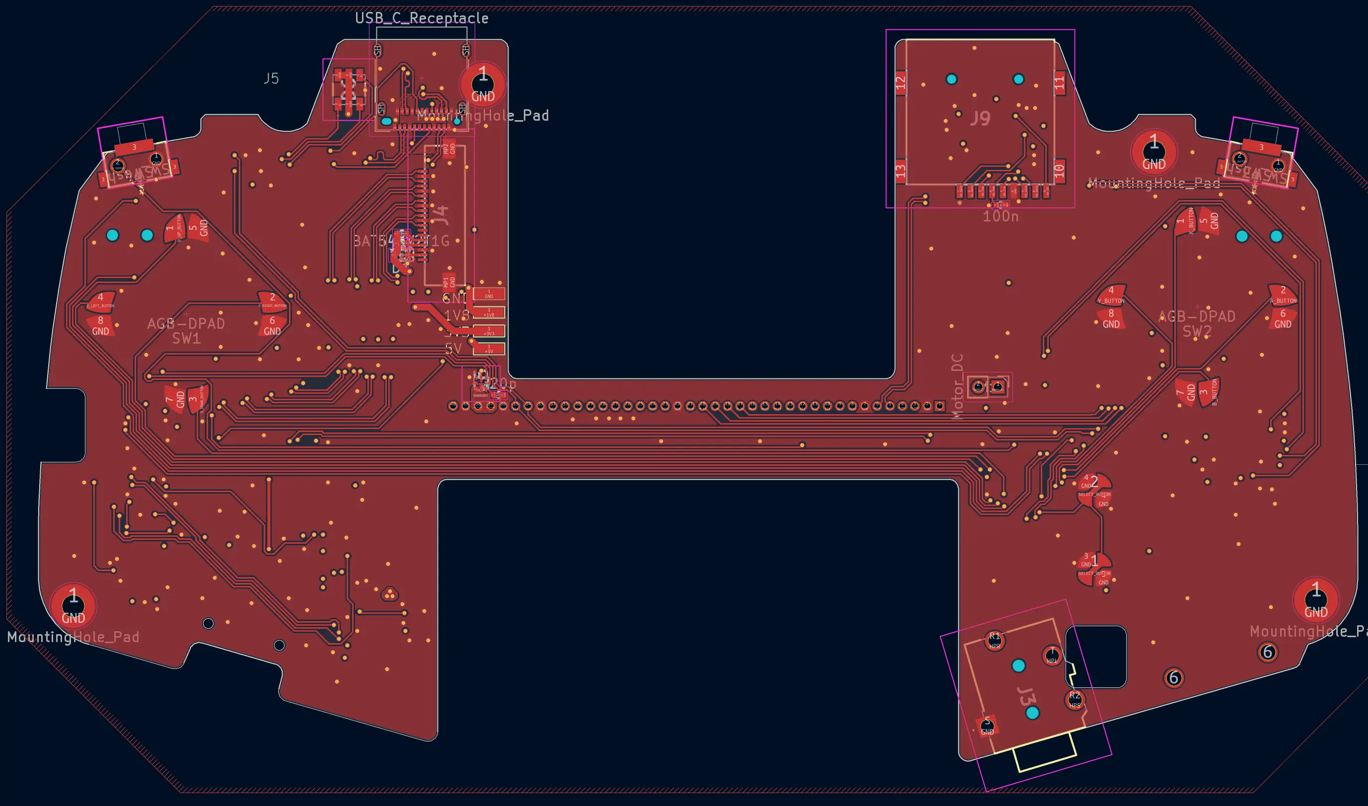
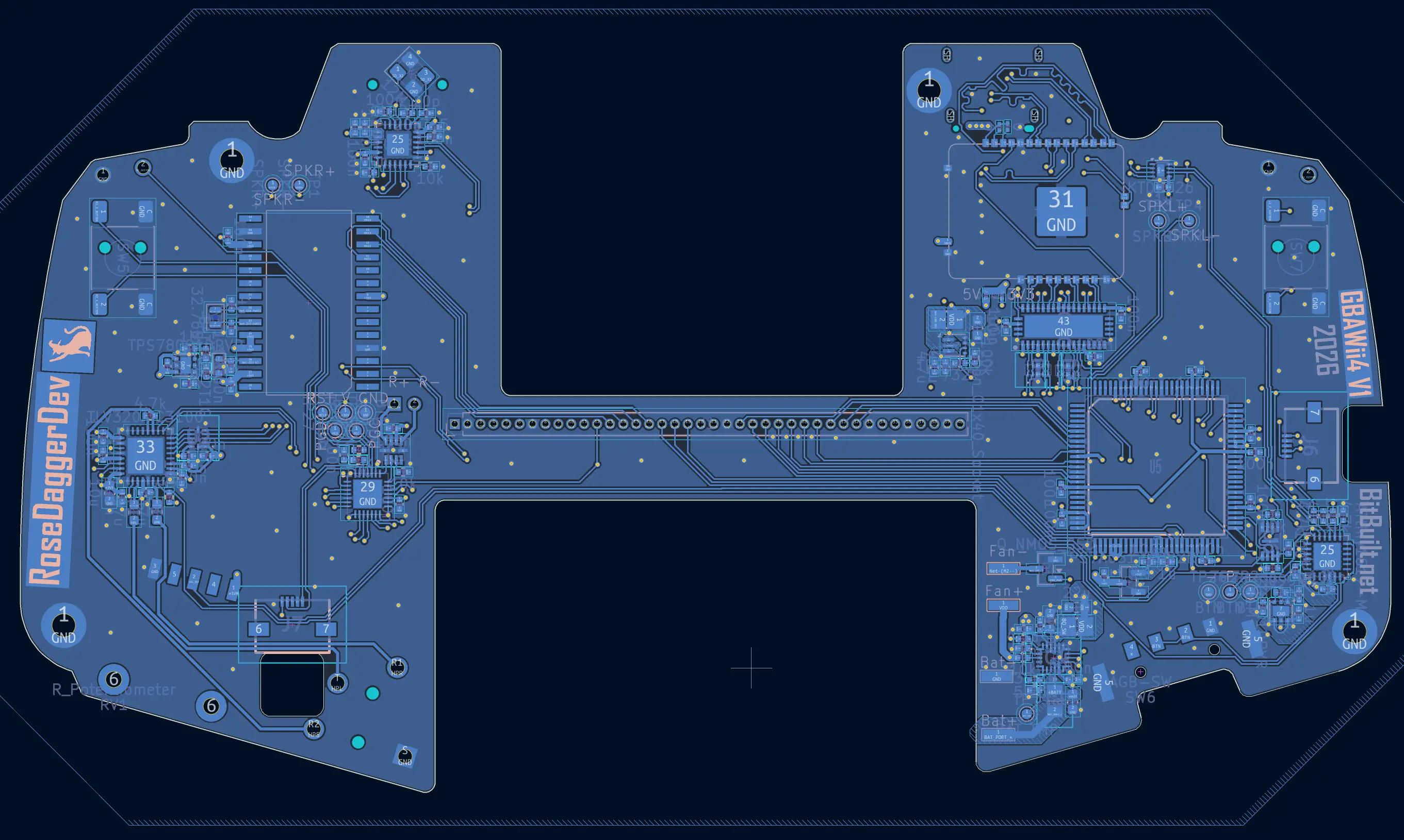
Now as for the timetable for this project.
Well, that’s enough for today, wish me luck. (*Pling*) Oh what’s that? DHL says they will deliver my package from JLC today instead of Wednesday like they had predicted?!
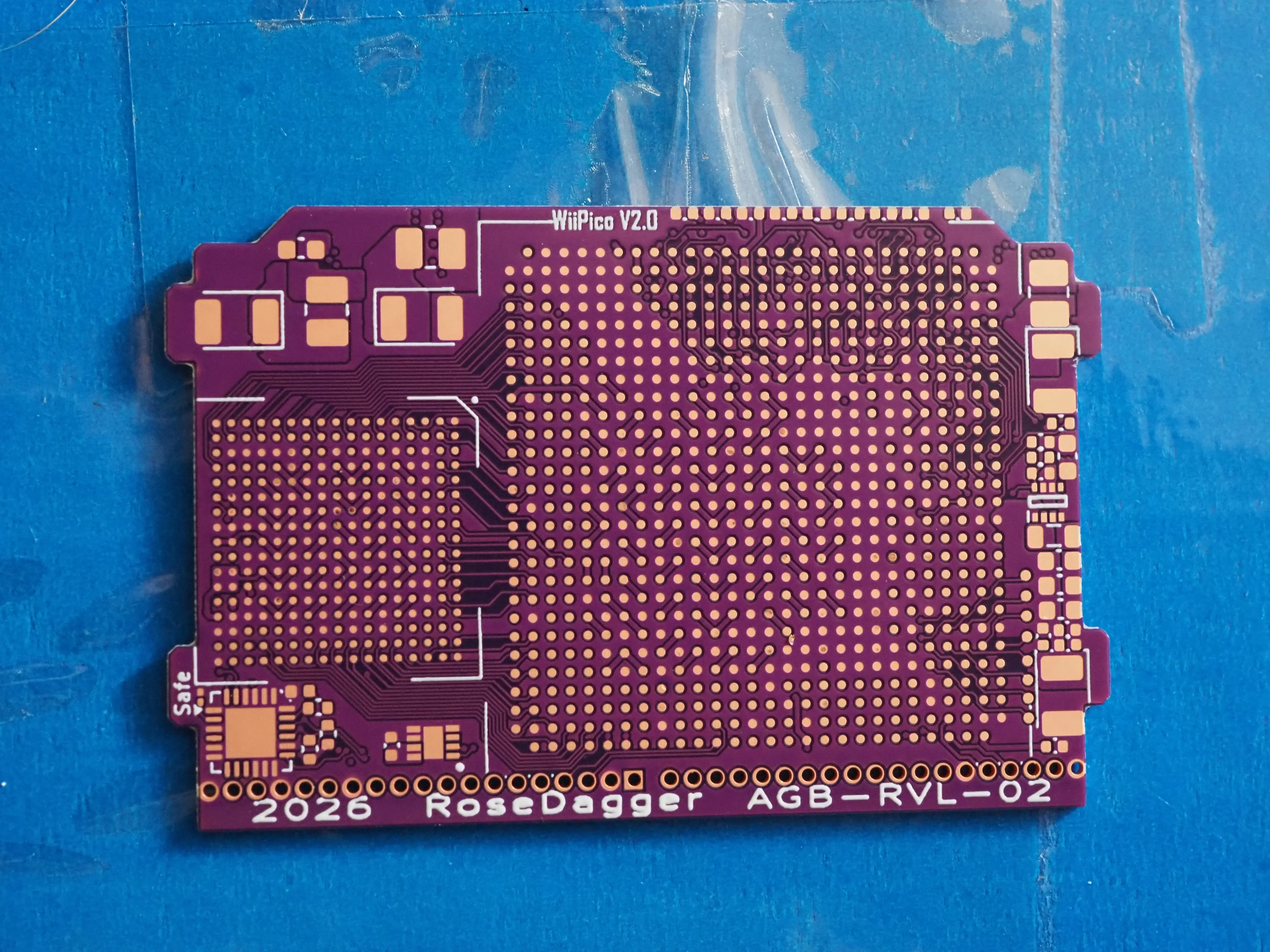
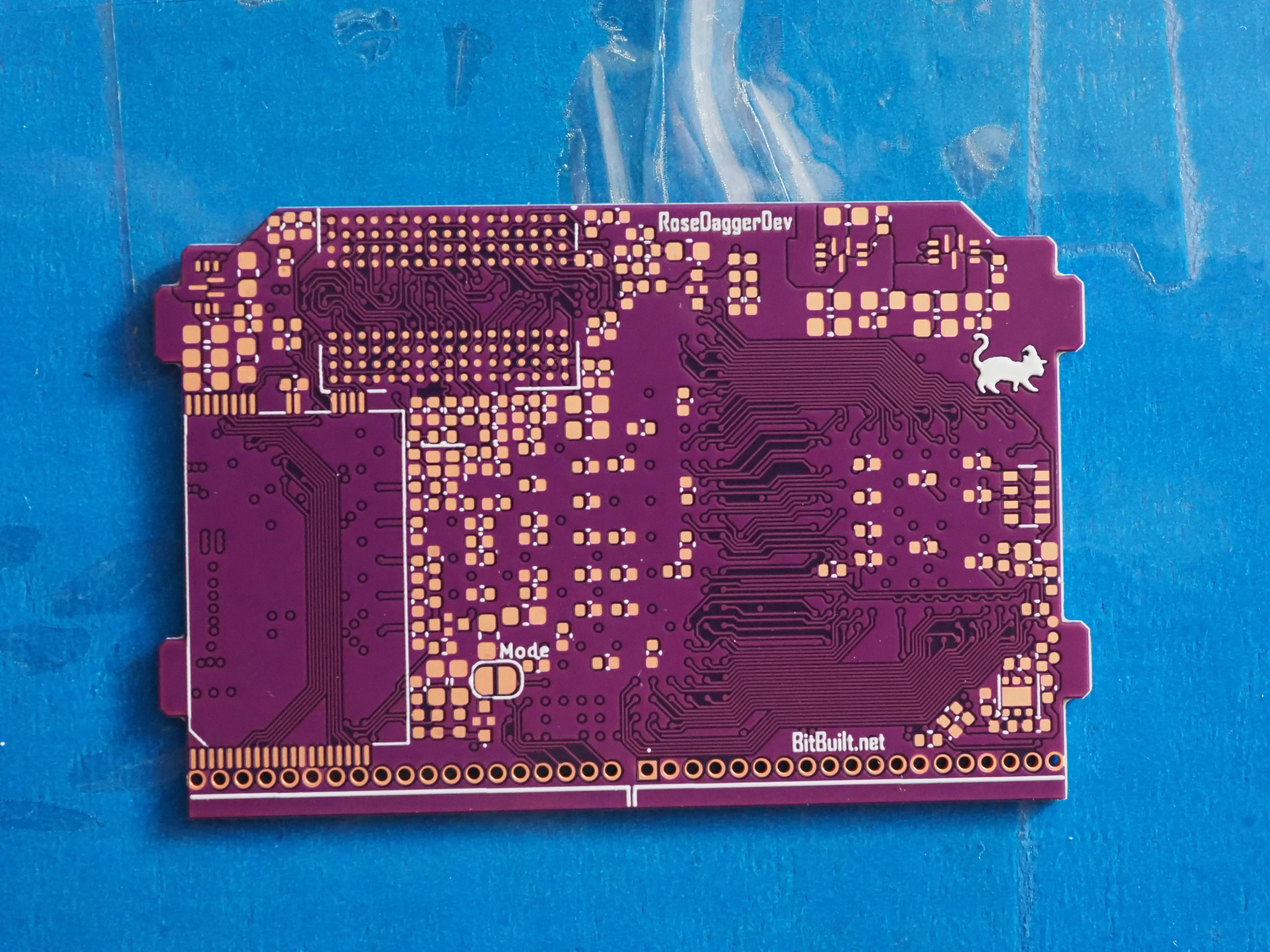
It does not change much as I need to finish baking and harvesting Foxtrot, but had I done that yesterday, then I could have saved a day off my timetable XP Ah well, Stellaris was still fun, so it’s fine XP
Edit: Forgot about the index card for my post, so here is Foxtrot after harvesting the chips. And I've learned I'll wait till tomorrow before I delid it XP
Part one: August 15th
Heya time for an update, and it’s a big one!
First off, I found out what was the issue last time, it turned out to be the NAND which was not properly soldered. I tried a few different things, including removing the CPU and checking all the pins, then removing the RAM, fixing the damaged solder mask underneath it, and checking everything there. Eventually I resoldered the NAND and... boom!
Now, that might not be the greatest image ever, but it’s an image! And you can see some of the details you expect from a Wii booting. Including how RVL is complaining about missing the USB drive. Now this image was a pain to get, the image would not sync properly, and I would lose the signal often, and touching the pins on the connector would change how the signal appeared, and how it behaved. With the connector being the main suspect, I tried touching up all the pins with my iron, and Tada!
Next, I just need to plug in the USB and we are good to go right?... Nope, it is not reading the USB drive… I check that I didn’t mess up D+ and D- or something else silly. But no, they seem fine. I check with an oscilloscope to see what’s happening, and it seems like I’m not getting a proper connection…
I’ve had a lot of connection problems between the PICO and the Dock… I wanted the PICO to be as small as possible, while using the normal GBA connector. However, the GBA connector assumes a much longer wiping/insertion distance than I’ve given the PICO, meaning that the contacts only connect at the very edge of the PICO, and any misalignment would make one side not fully connect…
After fiddling with it for a bit, I managed to align it perfectly and insert it at the perfect distance so that the pins made contact, and the USB could be read. Though this connector design is not great for what I need…
But it works! It fucking works!! Hallelujah!!!
Now let’s see if it can play anything. Starting with Super Mario Sunshine.
It runs! It works!! It can actually play games!!!
Now let’s see if it can play a Wii game, let’s try Mario Kart, as it has native GameCube controller support.
I played two cups back-to-back without any issues or instability!
I fucking did it! I have a working Wii on a PCB which is only 52x34mm! I moved the RAM to the backside and changed the DQ groups around and it fucking worked! I moved the CPU closer to the GPU and squeezed the traces together and the cross coupling didn’t kill it! The passives were moved around, and large sections are blocked off by the RAM and NAND so I could not place the passives optimally where they should go, but it still worked! It’s kinda insane that it actually worked with everything I changed at once XP
So I’m gonna call this conservatively a massive success as a prototype!!
Glory pics!
The testing setup:
Yes I ended up holding the heatsinks down with magnet wire and thermal pads
The Pico in the dock, with the 3.3 external regulator on the side. And plastic shims under the connector to give it enough force to mate properly.
I had planned to make the Video out and GC out into mini jacks, but then I forgot to order solder-able mini-jacks, so I just soldered directly on the terminals.
I had a handheld fan running over the setup to ensure it was cool enough to run.
Though there are some issues that I want to deal with for a second revision:
- The GBA connector really isn’t working well for the PICO. I have two possibilities:
- Extend the PICO by another 1-2mm to get the correct insertion distance to make good contact. That would bring the total height of the PICO in the cartridge to 39mm… The GBA cartridge that I’m trying to squeeze it into is only supposed to be 35mm tall, so I would be going quite a bit beyond that…
- Drop the GBA connector, and find something different, such as using pogo springs. It would let me reduce the height to 36mm, and it would let me add more pins.
- The flip chip DSBGA 3.3V regulator is a massive pain, and I want to avoid using it if I can. So, I want to replace it with anything else. Though the area I have to work with is very limited.
- I want to add “2026
NintendoAGB-RVL-02” or something similar to the PICO, as a further throwback to the GBA cartridge XP - I want to clean up some component choices.
- And importantly I want it to be purple! XP
Part two August 31st
With the success of the Pico prototype, I needed to kick my arse into gear. I had only a month and a half, to pull this off, on top of doing work. So, I down prioritized getting the update above out, which is why it comes half a month late XP
Now, however as I’m still busy, I’m gonna lightning round this:
- Connector: Pogo pins, and shortened the Pico by a bit
- Regulator: Replace with a tiny analog buck-boost
- Silkscreen: JLC said no, they don’t want me claiming to be Nintendo… Replace it with “2026 RoseDagger AGB-RVL-02”
- Component cleanup: Rewired the Tiny to align with the ThunderVolt more, changed the chokes, fixed the 100pF caps to 1uF caps, changed some inductors, etc
- Purple: Yes
I got a tip from YveltalGriffin to use a tiny non-I2C buck-boost he knew about and used that to replace the DSBGA and then use the DAC on the Tiny to adjust the feedback node. I had used that trick before on a different project, but didn’t think to use it here, and would have overlooked the absolutely tiny regulator he found. So, all praise to him for saving me from DSBGA hell XP
Also Pogo pins and targets are expensive as hell… I’ll not use them again if I can avoid them... Damn I really hope they work as I intend…
However, the Pico wasn’t the main work, I just wanted a minor revision on it to fix some issues and the connector. The dock or GBAWii4 was the main issue. I had a mock-up of it, the shape of the PCB was done, and most of the main components were added to the schematic. But I needed to go over it to fix any missing components and validate it. And then lay it all out and trace it. And I had a deadline… I ended my internship Friday last week. Uni starts up Tuesday next week. I have one week where I’m not in my final year in uni or working, so I got to make the most of it. Which meant that I needed to get the dock ready as quickly as possible.
And with a lot of blood, sweat, and exhaustion, I did it! Here is the GBAWii4 dock!
And inside the GBA shell: Yes the bottom cutout was for some larger fans and I didn't bother resizing the PCB after changing the fans.
And the copper looking thing on the bottom is the flex PCB from the display and display board.
With batteries:
There is a small riser for the pogo pins, I needed to lift them up. But it will also allow me to mount the pogo pins to the back shell where the cart sits and then connect it into the GBAWii4 PCB with the regular connector.
The routing could have been neater, I didn’t have much time to refine it or go over it again.
Now as for the timetable for this project.
- Saturday 29th: Finish the GBAWii4 and send it to JLC for printing. 3-4 days manufacturing, and 2-4 days shipping, would mean I could get them as early as Friday this week if I’m lucky. (Complete)
- Sunday 30th: Finish the GBAWii4 if I didn’t on Saturday, If I finished, start on Monday’s task, allowing me to move the week plan up one day. (Failed, I was tired and played Stellaris the whole day instead XP )
- Monday 31st: Digikey components arrive, Bake Foxtrot and write the worklog (In progress)
- Tuesday 1st: Reball the HW2 and CPU, and prep for the Pico to arrive
- Wednesday 2nd: Pico rev 2 arrives, solder all passives and small components
- Thursday 3rd: Solder the HW2, CPU, RAM, NAND, and check resistances.
- Friday 4th: If GBAWii4 arrives, solder it up. If not do finishing touches on the CAD for the Pico cartridge and send it off to be CNCed.
- Saturday 5th - Monday 7th: Test the Pico if the GBAWii4 dock arrived, or work on the CAD for the GBA shell.
- Tuesday 8th: Uni starts up.
- Debug and check the Pico and GBAWii4 works
- Write/modify firmware for the GBAWii4
- Any last adjustments if needed
- Get the Pico GBA cartridge CNCed
- Finish the design on the GBA shell
- Get the shell resin printed in translucent purple if I have time
- Print it at home if I don’t have time
- Assemble everything
- Final testing and showcase
Well, that’s enough for today, wish me luck. (*Pling*) Oh what’s that? DHL says they will deliver my package from JLC today instead of Wednesday like they had predicted?!
It does not change much as I need to finish baking and harvesting Foxtrot, but had I done that yesterday, then I could have saved a day off my timetable XP Ah well, Stellaris was still fun, so it’s fine XP
Edit: Forgot about the index card for my post, so here is Foxtrot after harvesting the chips. And I've learned I'll wait till tomorrow before I delid it XP
Attachments
Last edited:
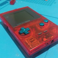
Wow this is actually crazy,good luck and can't wait to see the final result !
!
!
- Joined
- Sep 11, 2025
- Messages
- 58
- Likes
- 14
- Portables
- 1


- Joined
- Jan 15, 2021
- Messages
- 68
- Likes
- 267
- Portables
- Wii PICO (Complete), Wii Zero (WIP), GBAWii4 (WIP), GB Adwiince v3 Revenge (On Hold), GB Adwiince v2 (Dead)
Heya, maybe it’s time that I update? How long ago was the last update? 3 weeks? How long is left of the competition? 8 days? Yeah, okey maybe it’s time for an update XP
First let’s have a look at how my plan from the last post went:
The next part is going to be multiple different sections as I worked on a lot of smaller issues over the last 3 weeks.
PICO Rev 2
I finished soldering it up during the week off I had and it looks amazing if I say so myself ^^
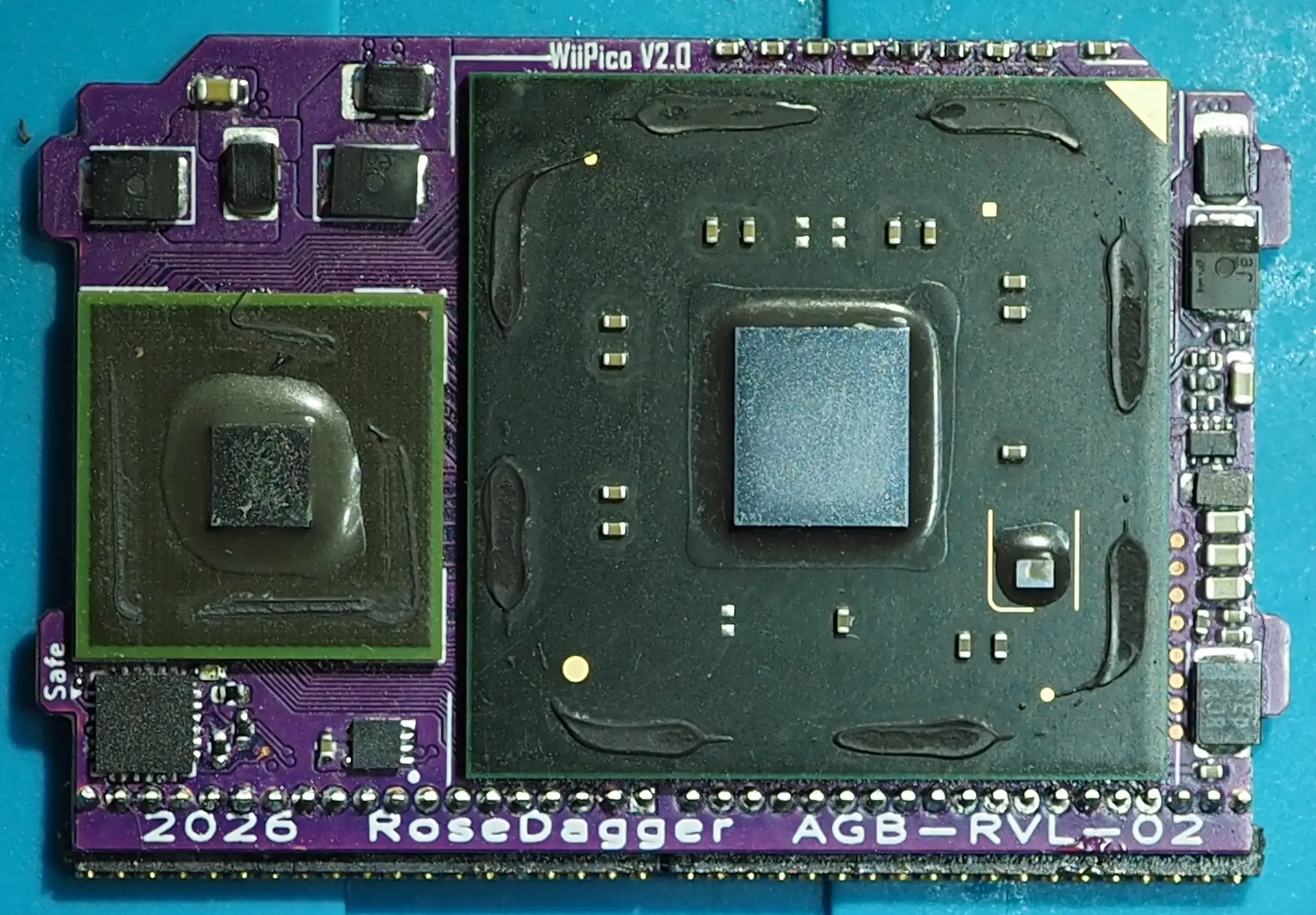
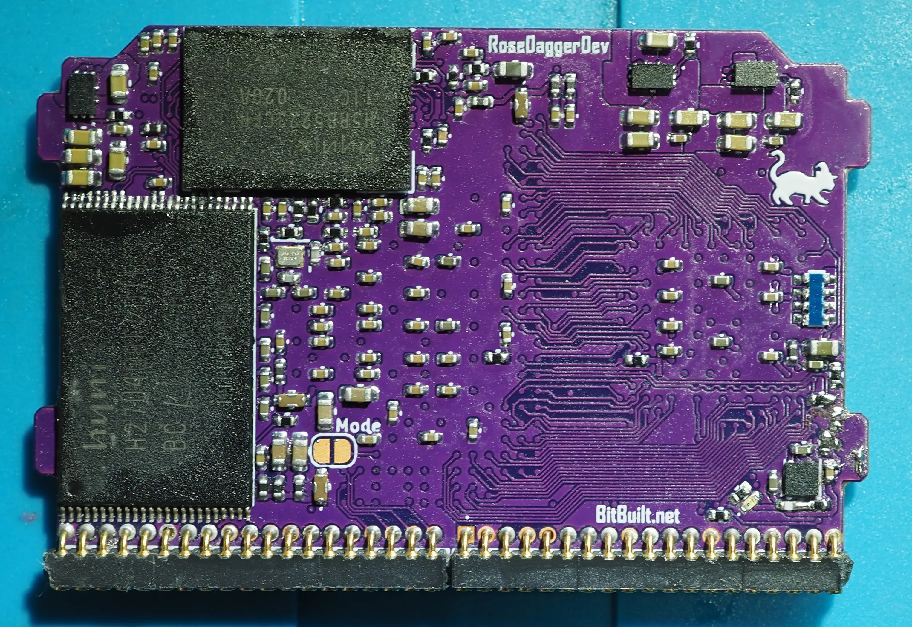
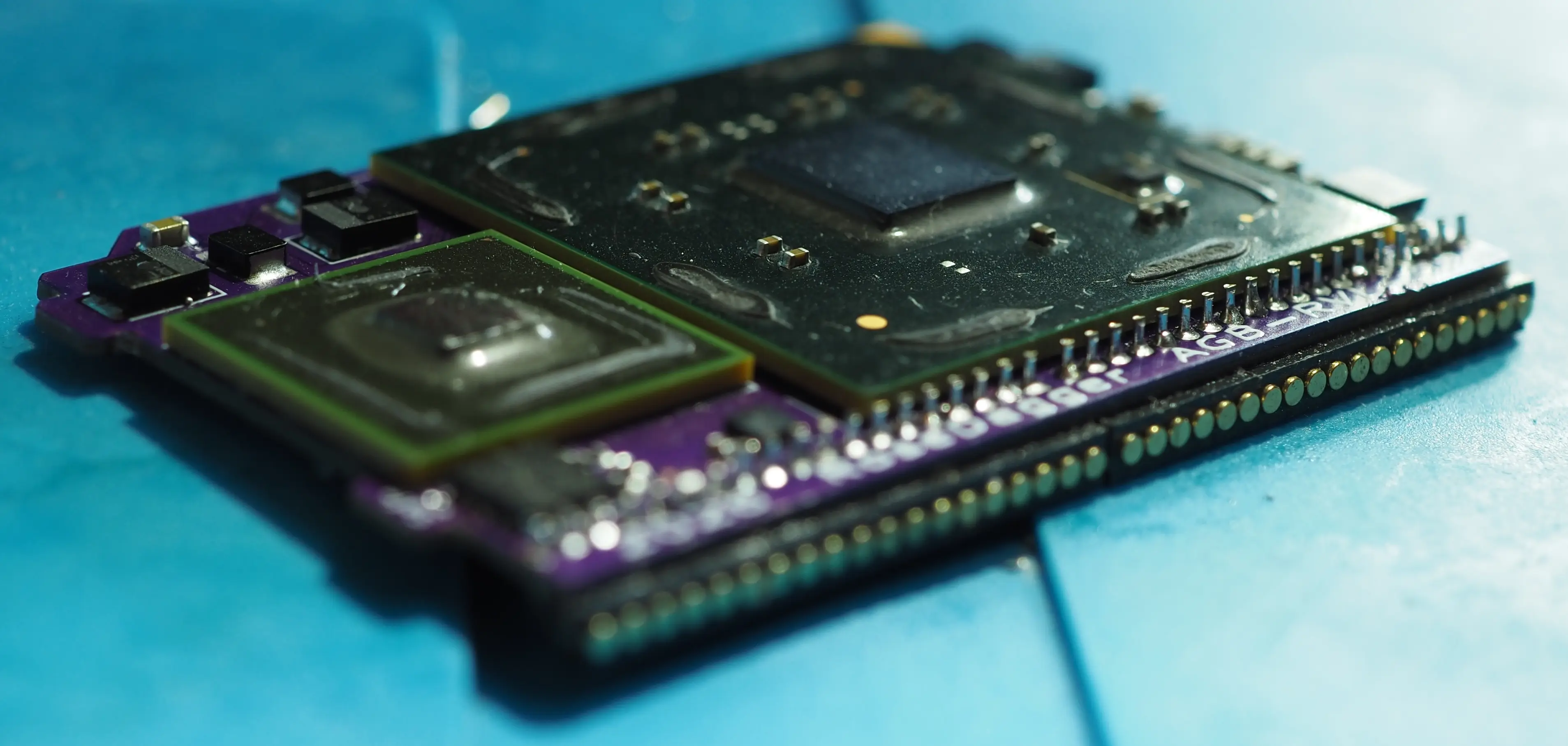
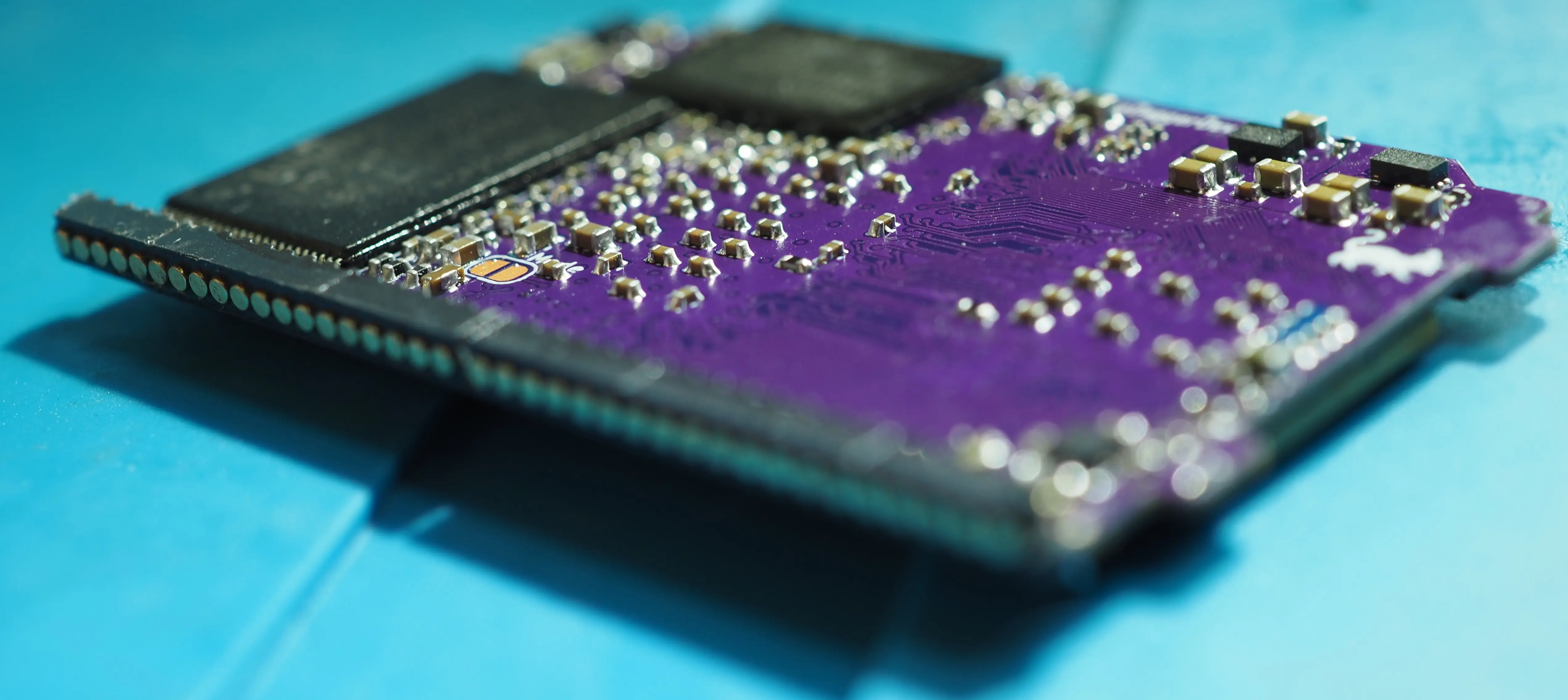
Now as for how to test it. It was still my week off, and I didn’t have the new dock… But I wanted to test if it worked… The old dock used a different pin spacing and connecting interface so I can’t just plug it into that now, can I?
Hmmmmmmmm… Even though the pinout changed the main features remain the same, what if I just solder some magnet wire on the video and power pins and hand wire the Pico Rev 2 to the old test dock? That should work, shouldn’t it?
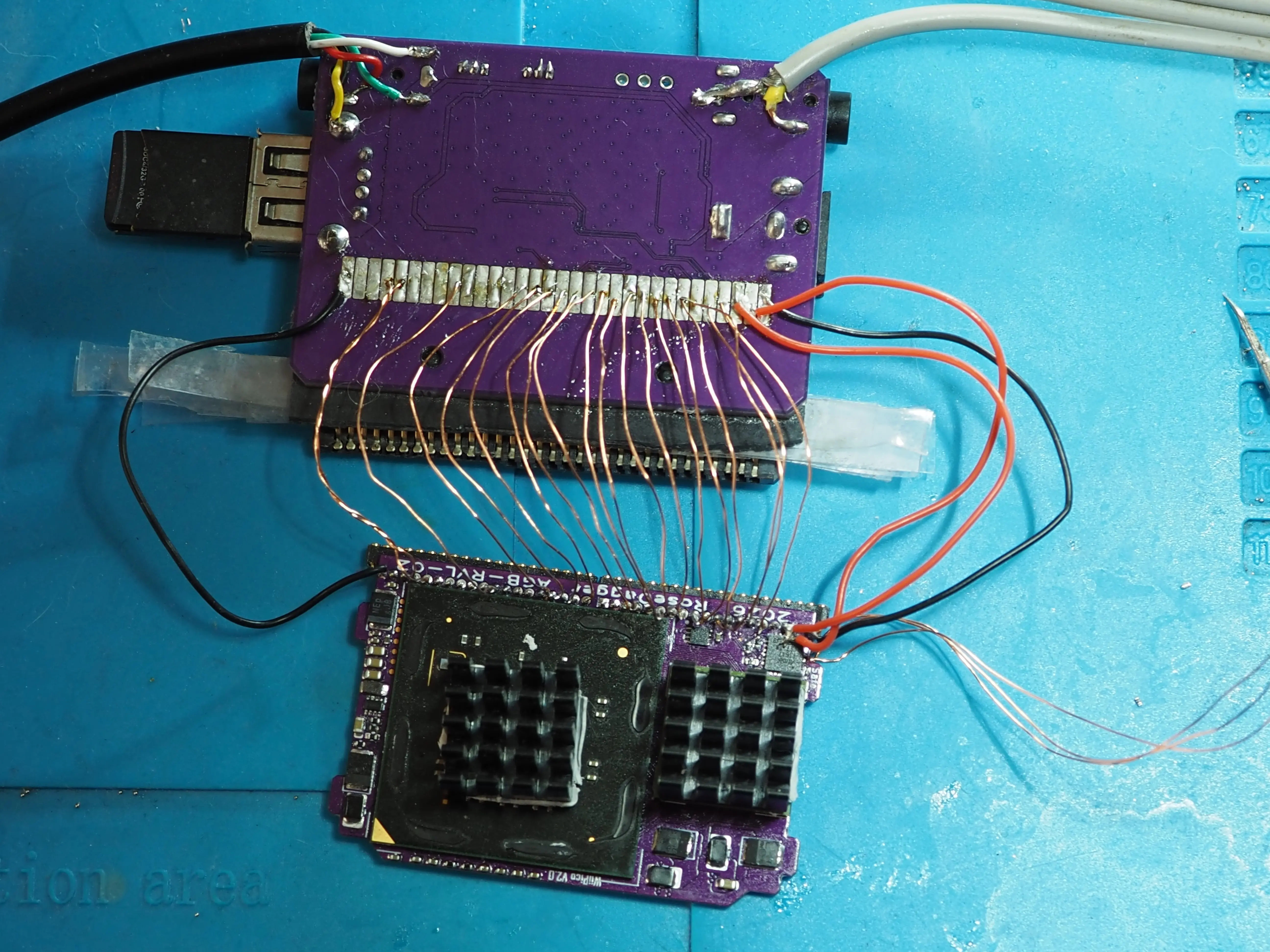
Hmm that worked surprisingly well! Now let’s see if it boots?
Do I get power? Check!
Does the GPU and CPU heat up? No…
Do I see any reasonable activity on the data or clock lines? Nope…
Let’s check U10 reset? 2.3V… What?
Okey I know what’s going on here, and I’ll explain.
So while changing the ThunderVolt source code to work with the PicoThunder (aka my implementation of the ThunderVolt on the Pico). I discovered that there was an option to emulate U10 without using a MOSFET. It would instead wire the reset line directly into a pin on the Tiny, then it could pull the pin low to reset, and set the pin to high impedance to let the GPU pull the line up to 3.3V. It seemed brilliant, I loved it, and since the MOSFET on the Rev 1 had been one of the things I failed to solder initially, it would remove a potential fault source. So of course, I removed the MOSFET for Rev 2 and used this emulated U10. However, there was one aspect that I had not considered. The Tiny runs on 1.8V, the reset line is 3.3V, the voltage protection on the Tiny is VDD + 0.5V. 1.8V + 0.5V is for those who are good at math, less than 3.3V. It’s 2.3V to be exact…
Now this is a tiny little bit of an issue, as 2.3V is apparently not enough for the GPU to go out of reset…
The obvious solution is to place the MOSFET back. Don’t fix something which isn’t broken. However I had removed the footprint completely, so my other option was to cut the trace, solder some magnet wire to the traces, and solder on a MOSFET. The trace width is 0.1mm, my magnet wire is 0.25mm in diameter, the MOSFETs I had in my backup pile is a tiny 1x0.6mm MOSFET with tiny pads… Yeah no I don’t feel like soldering that XP
(Now that I think on it, I could have used the U10 MOSFET from the Wii, that would have been easier to solder, but I didn't think of that at the time.)
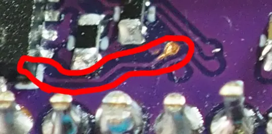
Now the other option was to increase the VDD on the Tiny. The voltage comes for a small LDO which uses a resistor divider to set the output voltage. The 1.8V is only to make it use less power, while the tiny is fully capable of going higher. Checking my book of 0402 resistors, I can make the LDO output 3.04V. 3.04V + 0.5V is in fact greater than 3.3V. I could have gone a bit lower, but it would mean replacing both resistors, and this worked, so (shrug). It will use a little bit more power, but it should be fine, everything else connected to it is 3.3V tolerant so it does not really matter.
For the public release I’ll put the MOSFET back, and call it Rev 2.1. XP
Now does it boot? Nope, it does not seem to be able to maintain the main clock. Last time I replaced the caps on the main crystal. But didn’t this time. A quick swap of load caps and the clock is running. I’ll fix that for the public release as well.
Does it boot now? Ish… It clocks are running, it heats up, but the video clock is 27MHz… I’ve seen that before, so I poke each leg on the NAND to see if they are soldered. Don’t see any of the legs moving… I measure again… 54MHz! I connect the monitor, and behold:
It seems of all components on the PICO, it’s the NAND I struggle with the most XP
But I’ve proven that the Pico Rev 2 works and only needs some minor fixes which I don’t need a new print for. Whoop!!!!
Pico Pak
Did you know the official name for the Gameboy cartridge is Gameboy Game Pak? As such I named the cartridge for the Pico, the Pico Pak.
Now I had done most/all the design a lot earlier, I just wanted to measure the final Pico to be triple sure the dimensions would be correct, then go over and round all edges.
I had fought for every fraction of a millimetre of space in the height direction, so that the GBA connector would fit, even delided the chips just to get slightly more clearance. And I had cut into the top and bottom to the maximum thin wall limitations for JLC.
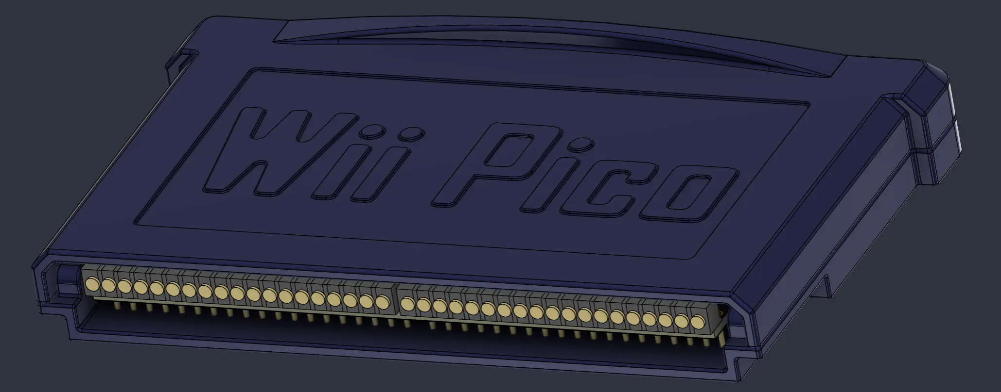
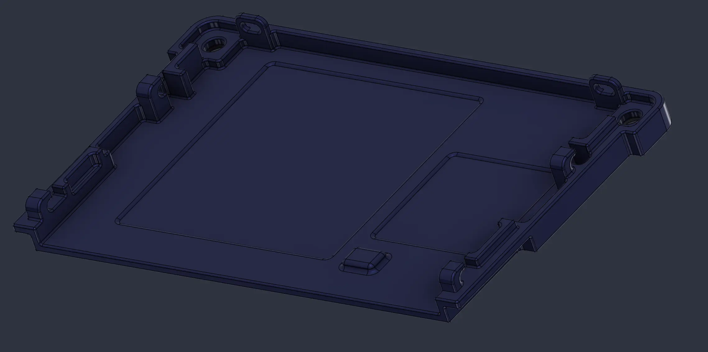
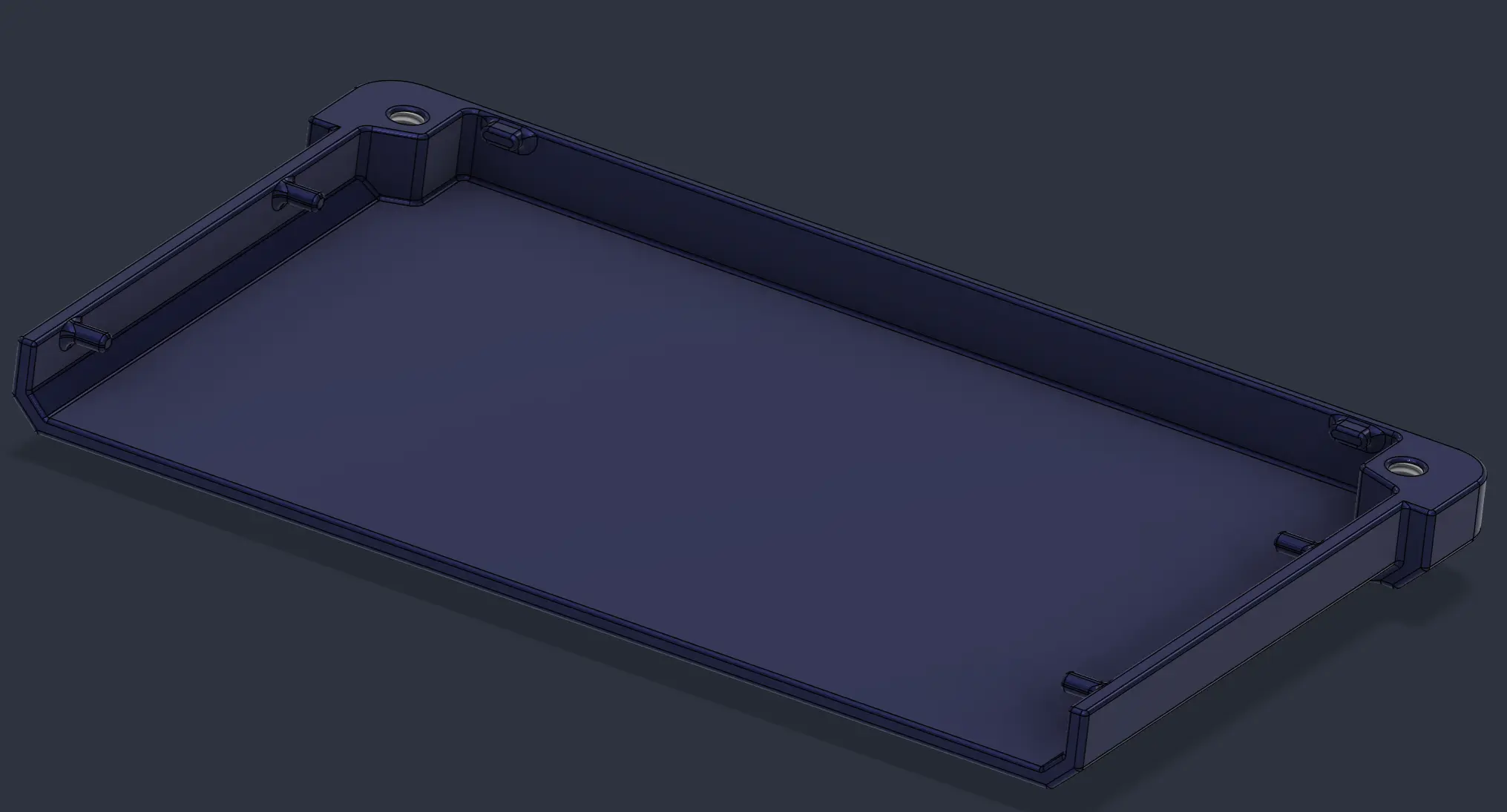
I had also made this really cool locking mechanism, where the two pieces would slide together and the hooks would interact with the pegs. Locking it in all directions, and the screws were only needed to make sure it would not slide apart. And it worked well 3D printed!
So with all finishing touches done, I sent it off to JLC for CNCing to see if they could machine it.
Nope. They didn’t like the pegs at they could not give me undercuts. And they didn’t like that all wall thicknesses were in the “thin wall” range. Apparently, you needed some normal walls to provide enough support or something XP They wanted the main top/bottom surfaces to be 1.5mm thick at least… They were 1mm thick with some parts recessed to 0.8mm… All my efforts to gain every bit of height were wasted. And the GBA connector would never have fit XP Good thing I had switched to the pogo pins, right?
Shit… I’m getting squeezed and it does not fit… Fuuuuuuuuuuuck… I ask JLC if they will allow some cutouts in the main surfaces below 1.5mm as long as most of it is 1.5mm? And they answer that yes that is allowed. Okey cool, maybe I can save this? What if I flip the connector around to the top? There it would have more space…
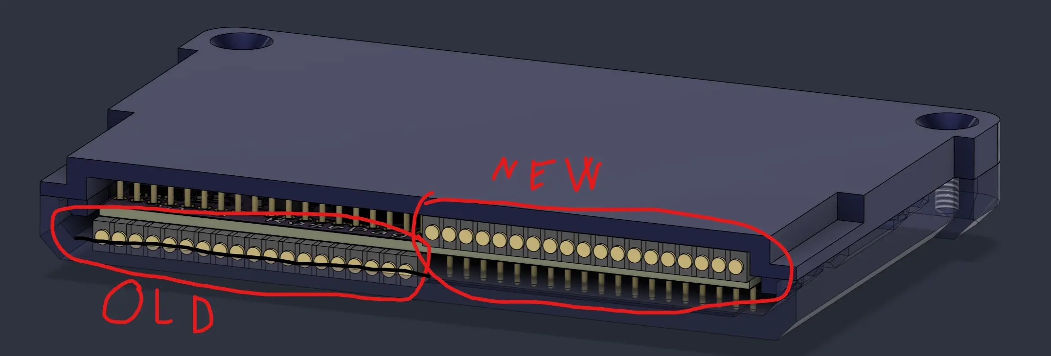
Yeah, that would work! Hallelujah, the main design will still work!!! It would cover up the AGB-RVL-02, but that is fine. Though there was a second issue… All these changes would of course mess up the height of the riser for the meeting pogo springs. But that is a cheap 2-layer board, so I can have that reprinted. But it means I can’t test the Pico with the new dock when it arrives… But oh well, I already know that it works due to testing it with the old dock.
Now over to the second issue… No undercuts… My hooks and pegs won’t work… But I want some more support than just the screws… Guess I’ll just make some tabs which goes down and meets surfaces on the other side, locking it in all directions except straight on? And then the screws hold it in in that direction?
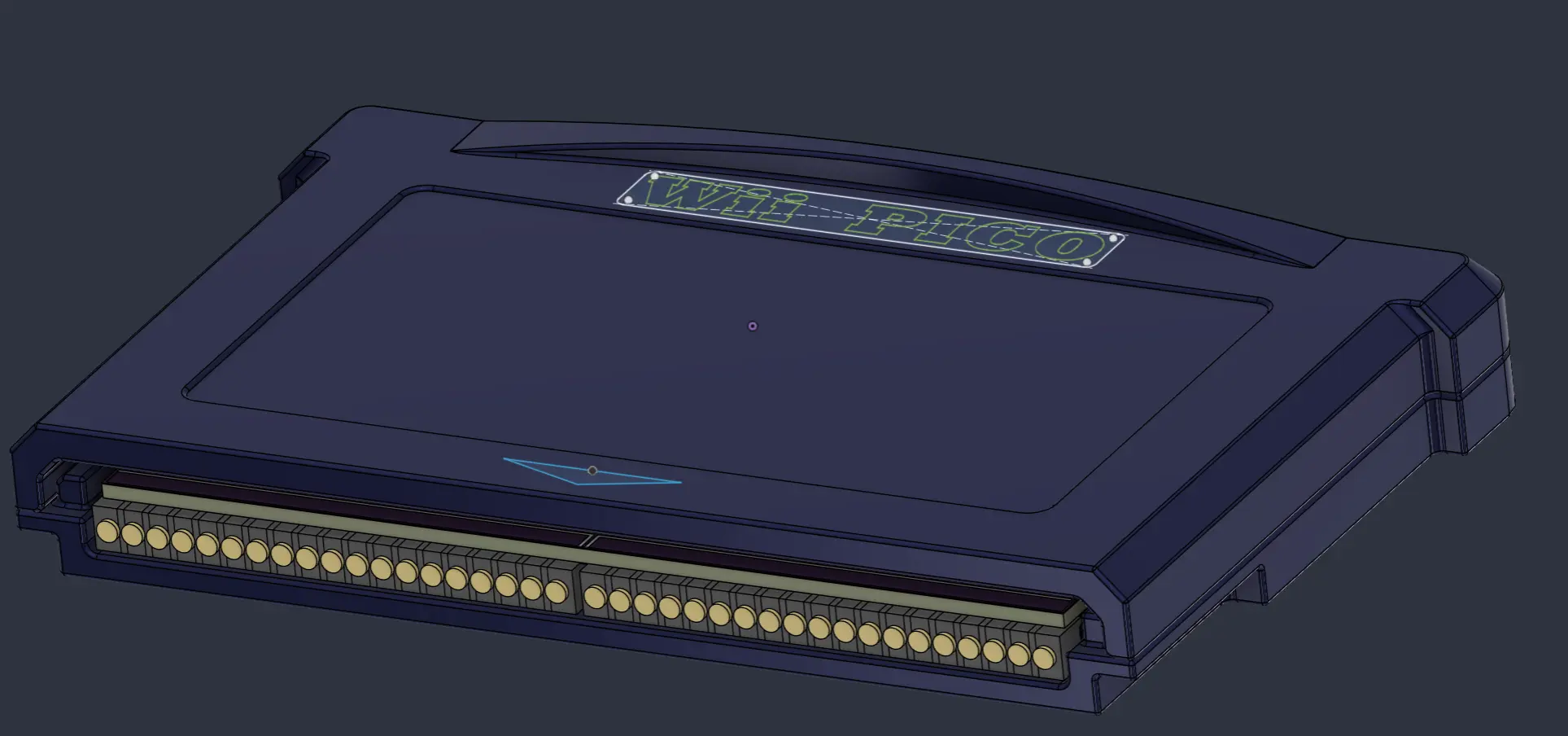
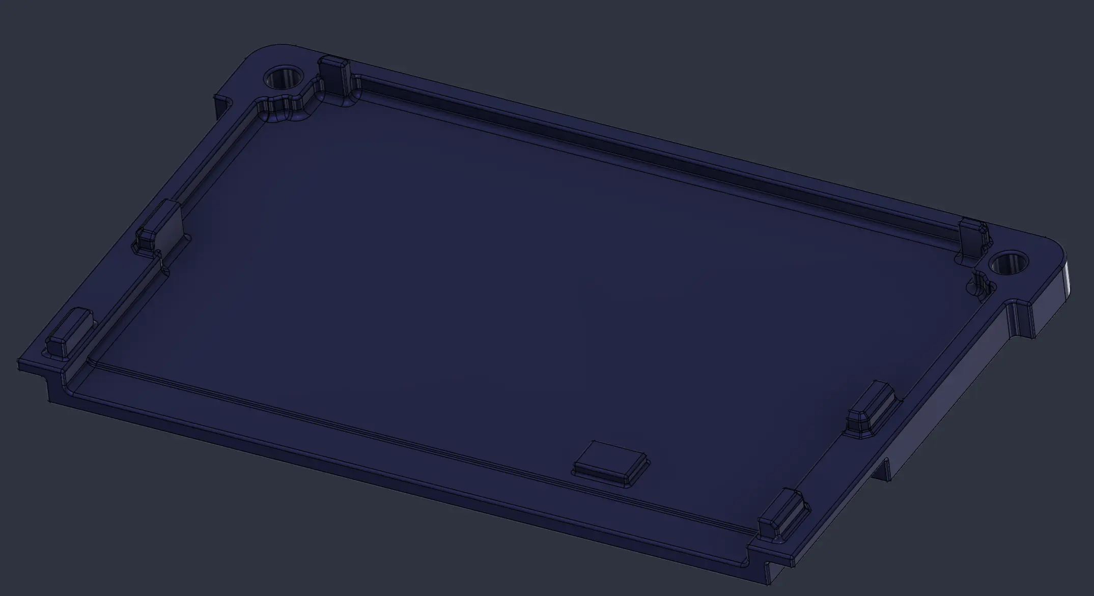
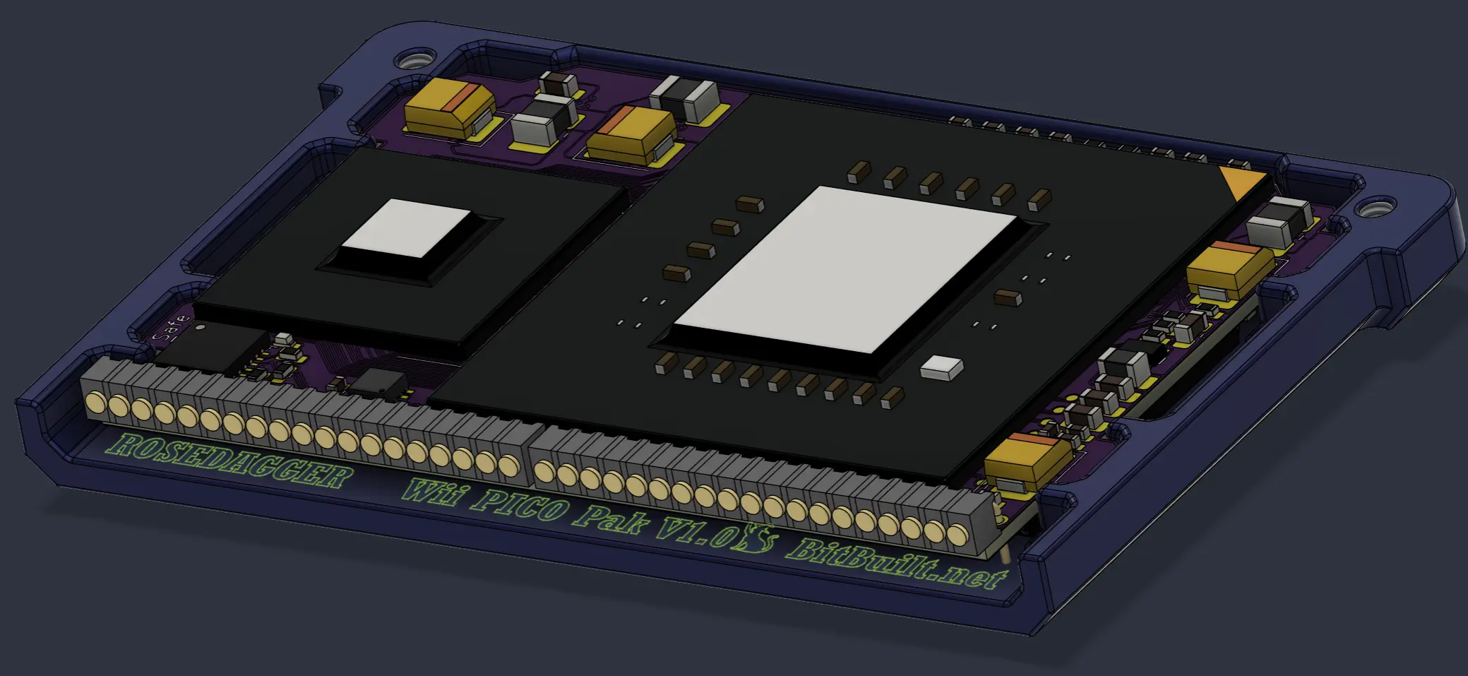
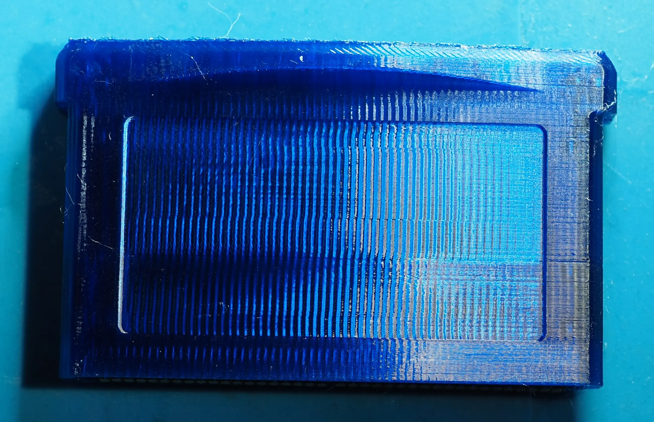
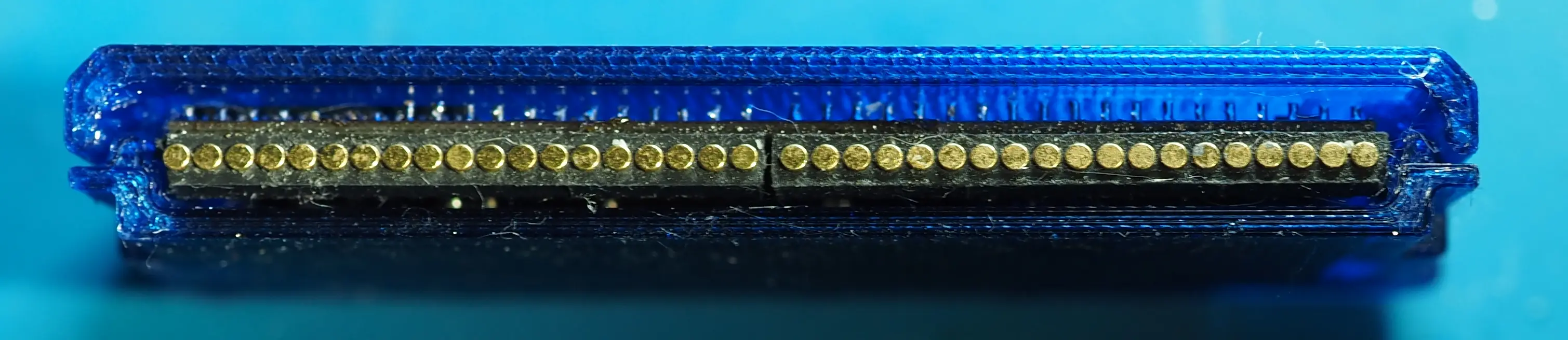
Well that seems to work!
Now… Since I was already changing the design… I figured maybe I’d add some more details? I had added the Wii Pico as a raised section in the area where the GBA game label was supposed to be. Mostly due to that cutting the letters into the area where Gameboy Advance is supposed to be, would have been too small for the cutting bit. And I didn’t know how to make a technical drawing for lasering. But to tap my screw holes I needed to learn to make a technical drawing… So why not laser? XP
Now it was fully done, so I sent it back to JLC, and they approved it! Whoop!
GBAWii4
Now onto the GBA dock, I got the PCB back and soldered it up without too much hassle.
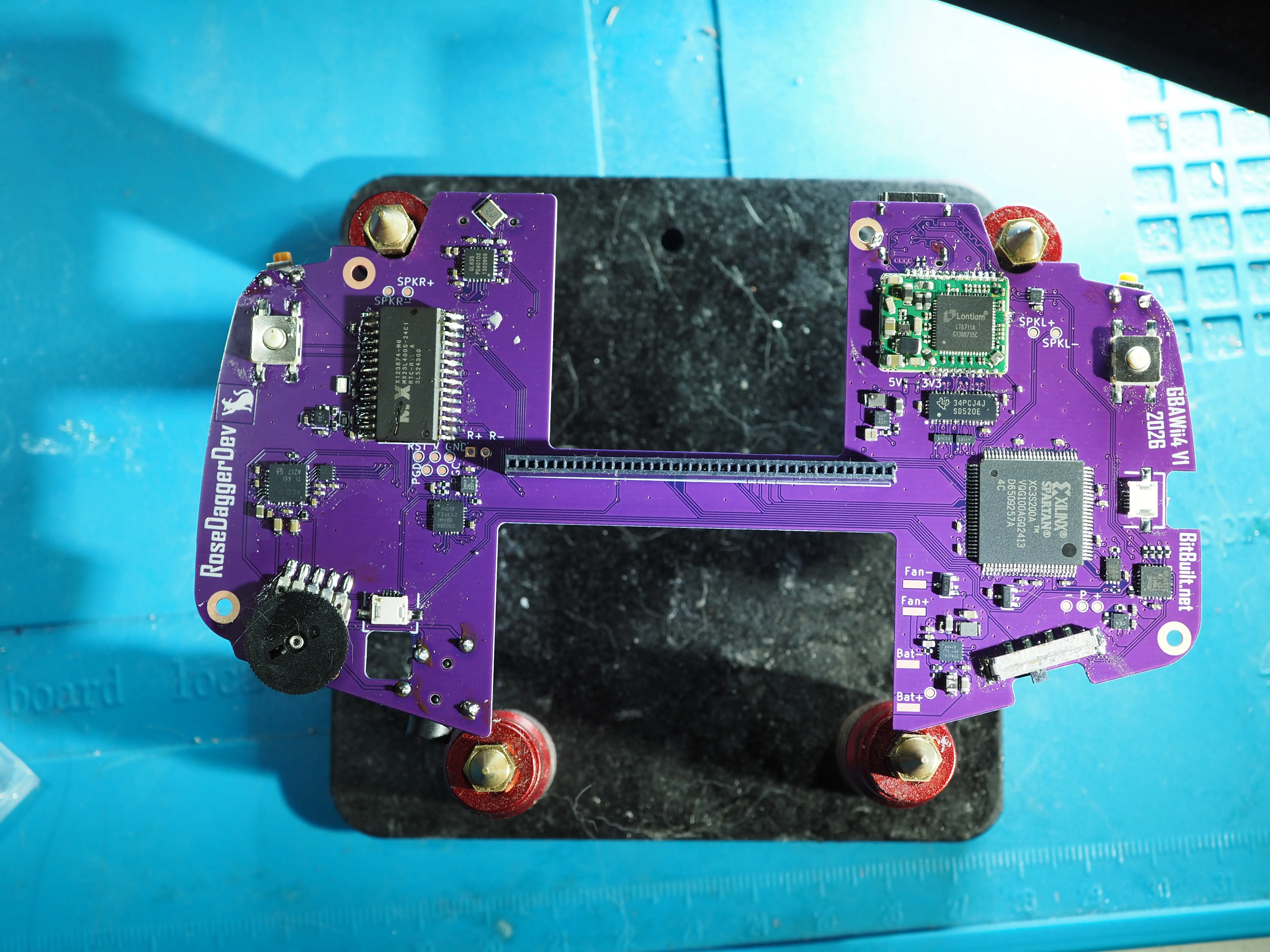
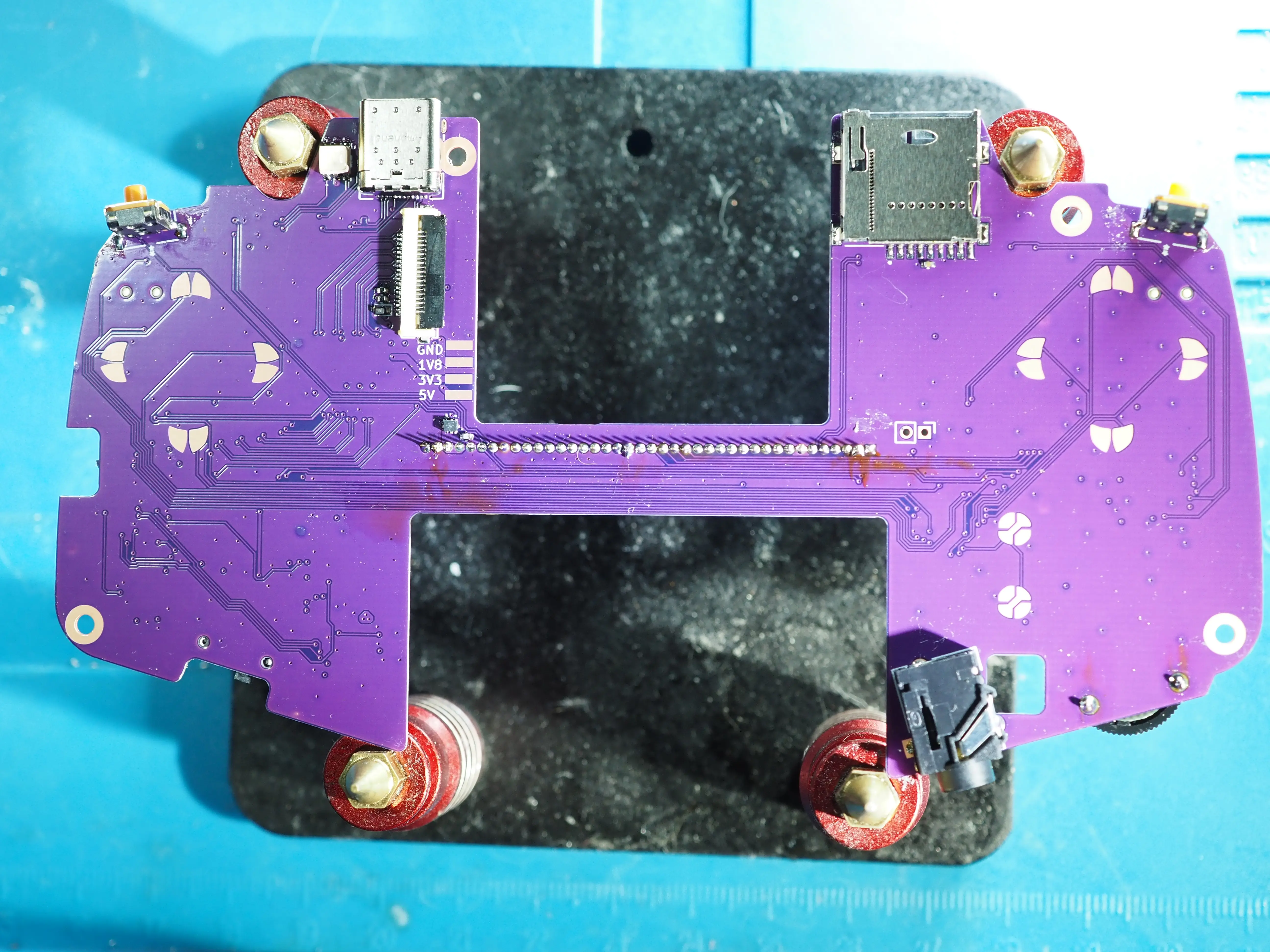
Some firmware writing later, and I could control the RGB light, the 5v regulator for the display. (I can very likely run the display of 3.3V and 1.8V, but I don’t have time to check). The power switch for power to the PICO. And the charging controller. One tiny note, apparently the “Absolute input voltage regulation limit” is the absolute minimum voltage, not the absolute maximum voltage… I set it to 16V and then ended up confused why it never tried to charge the battery. Changing it to 4V and suddenly it was happy to charge XP
The only bits left to test requires that the Pico is inserted. The dock feeds battery voltage into the Pico, and the Pico feeds 3.3V and 1.8V back out using the regulators on it. So, anything connected to 3.3V and 1.8V requires the Pico.
Well, there is one thing I can do while I wait. I can program the PIC for GC2+. I connect it up to the programmer, and try to program it… MPLab is throwing some errors… It is expecting a PIC18F25K42, but I have a PIC18F24K42… That’s odd, but surely, it’s not a big deal, I’ll just update the targets in MPLab and flash it… Now it is complaining that it does not have enough space… The F25 has twice the space of the F24… And GC2+ uses most of that space… Yeah no I’m not fitting it on my PIC… Why do I have the wrong PIC? I copied it from my previous design for last year’s contest… Let me check the source schematic for the GC2+… It needs the F25… I have no clue why I picked the F24… I did it last year and never reached the bring up stage to notice the issue. But oh well. I have the GC2+ from 4-layer tech from when I did my first contest entry in 2021. Maybe I can just use the PIC from there? Nope it’s the wrong size… I got to order the correct one… Oh well there’s enough time at the point I discovered the issue. Good thing I tried it when I did XP Now let’s just hope there’s no other issues as I won’t have time to fix them…
Wii Zero
One night I lay thinking about the title for the smallest Wii in the world. The Pico in the Pico Pak would be the smallest Wii motherboard, in the same way that the Kawaii is the previous smallest. But both require a dock… And I have more stuff in the dock… So my claim to be the smallest always comes with an asterisk… The TV dock was supposed to fix that, but I abandoned it… But maybe I could unabandon it?
I took a look at the test dock… It’s very sparsely populated, and about the same size as the Pico Rev 1. I have the Pico Rev 1 still laying around and it works. The main issue was the connector and the 3.3V regulator… What if I quickly made a new dock for it, which I could hard solder the Pico Rev 1 to? It would not be in a GBA Pak, but it would let me stack the PCBs. And if I feed 3.3V into VDD on the Pico, then I can remove the 3.3V regulator completely and just solder a jumper between VDD and 3.3V.
So, I got up and made an ultra-quick mock-up. Using the footprint of the Pico Rev 1 as my max PCB size, and tried to see what I could fit in.
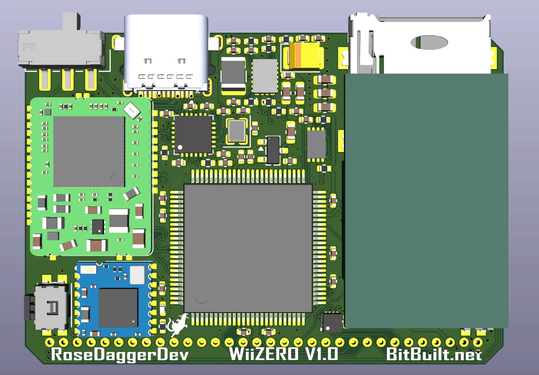
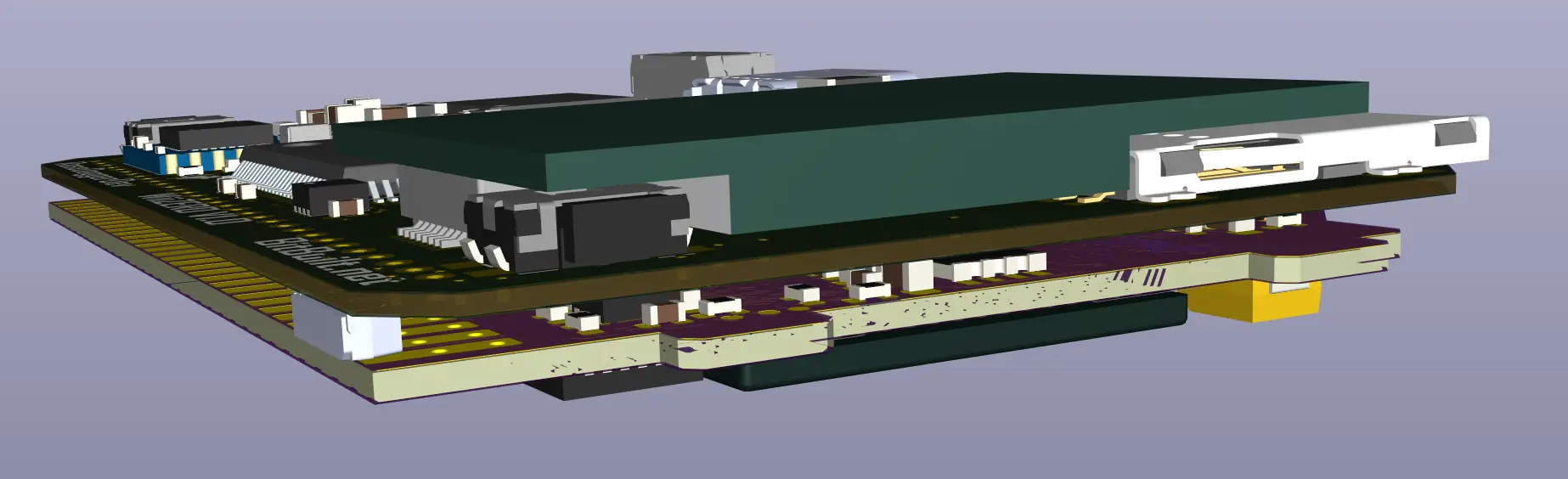

So, this fits inside the bounds of the Rev 1, and it is GCVideo, straight into MelonHD. For USB C DP out. It gets PD in and feeds it through a 3.3V regulator. It uses WavePhoenix for controllers, and the Bluetooth module for Wii motes. And the GL827 for SD to USB. The only ports on it are the USB C for power and video out, and the SD card slot. And it all took about 24h from I thought of it, till I was ready to order XP It’s mostly just reusing parts from different projects and then playing Tetris for a few hours.
Now why did I do this when I’m already swamped with stuff to do? I wanted to fully claim the title for the smallest Wii in the world without any asterisk or caveats. The Kawaii, the smallest Wii which requires a dock is 60x60x15.8mm. This Wii Zero, would be just 52x36x7.2mm! Sure, I would need a case and a heatsink, but I would still, without any question be the smallest Wii in the world! And that was kinda the point of making my own PCB and moving the RAM around to the backside.
The Pico Rev 2 will be the smallest Wii motherboard which requires a dock. While the Wii Zero will be the smallest self-enclosed Wii in the world! Yes, I’m greedy and want to steal all the titles XP
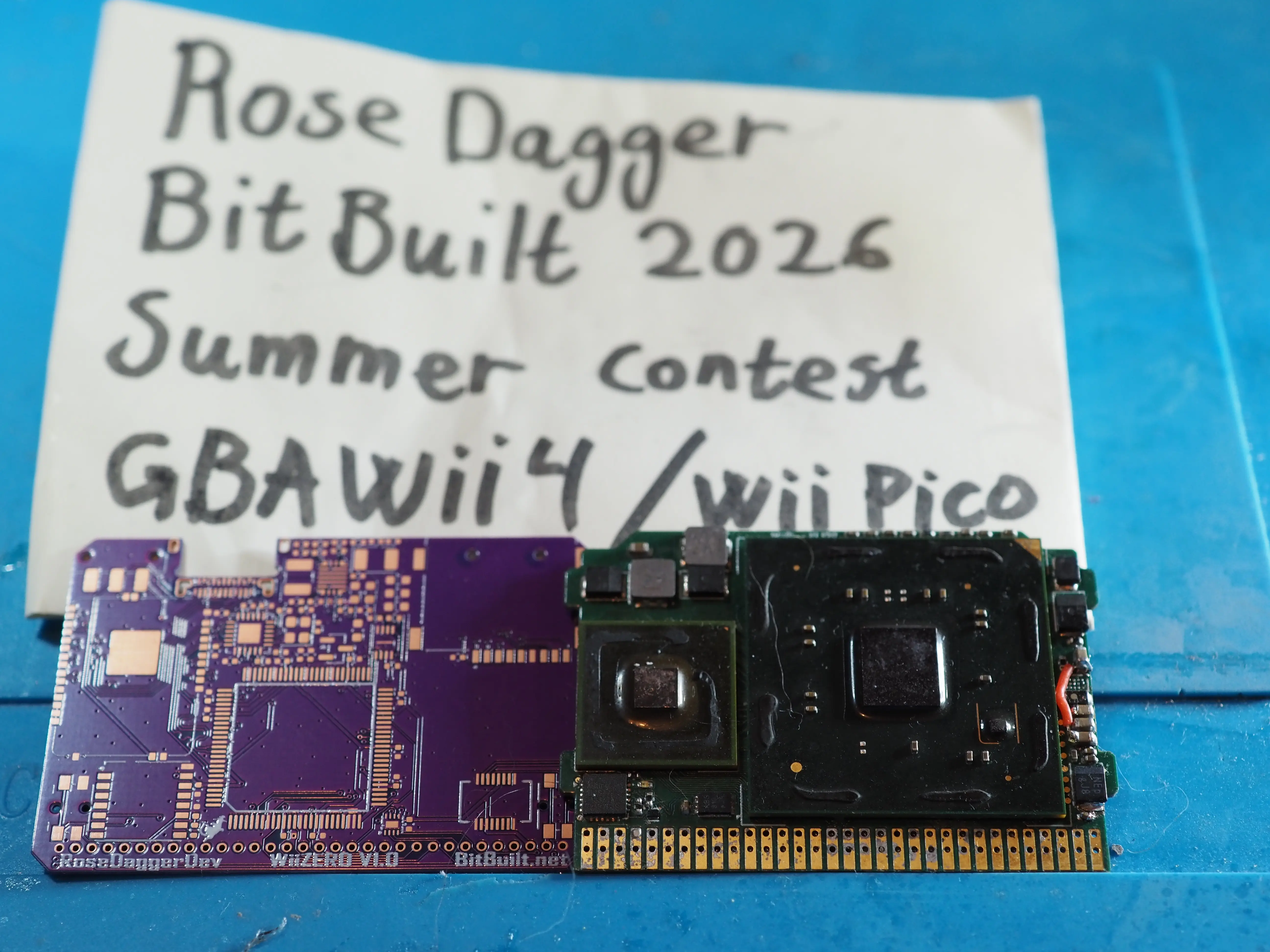
Can we go smaller?
There was a small discussion in the discord about JLC adding HDI vias, aka buried and blind vias.
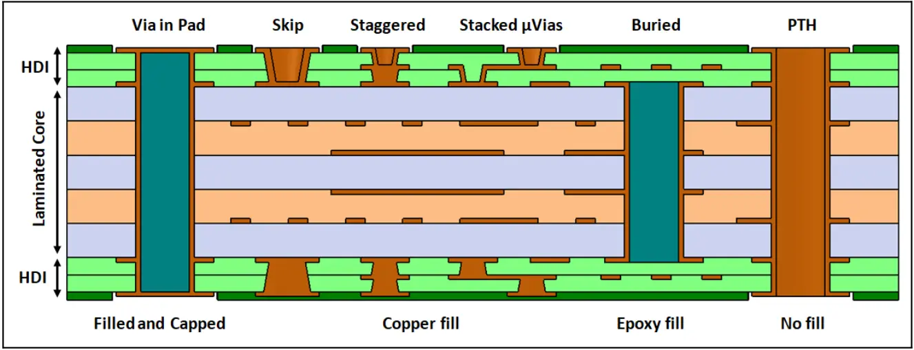
And if it was possible to make the Pico even smaller… So of course, I made another ultra quick mock-up XP This is the CPU also flipped around to the back. And all passives as 0201. It all fits within the footprint of the GPU XP It would be hell to trace it all and would need to use HDI which would be even more expensive than what I’ve done so far. But it is technically possible to fit it all. Will it work (shrug) all the passives would be in the wrong spots, and all traces, lengths, and impedance would be off. But maybe. I proved that it worked for the RAM, and that is higher speed than the CPU.
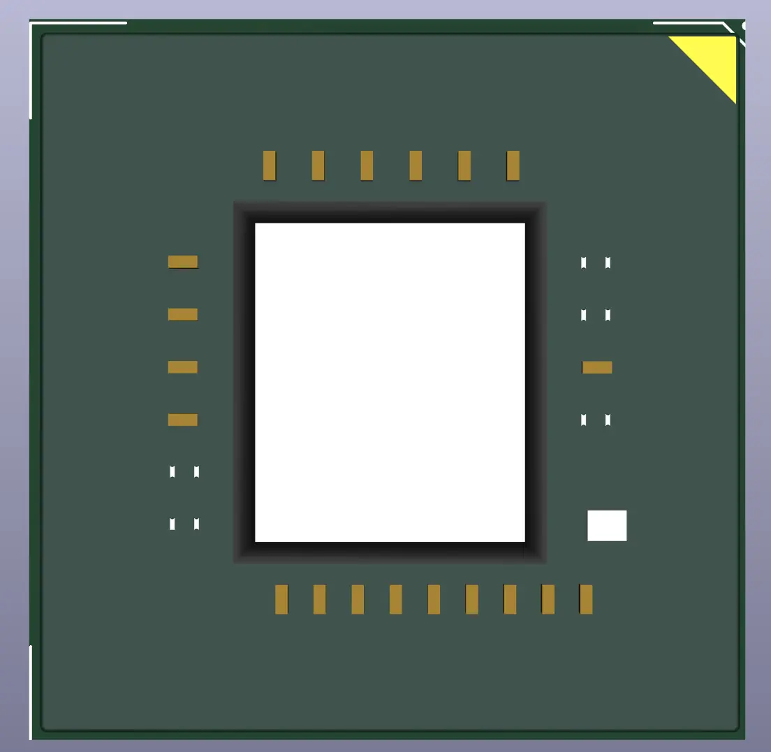
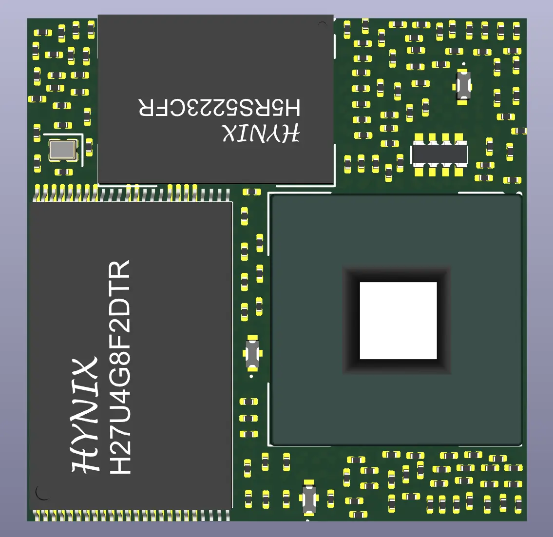
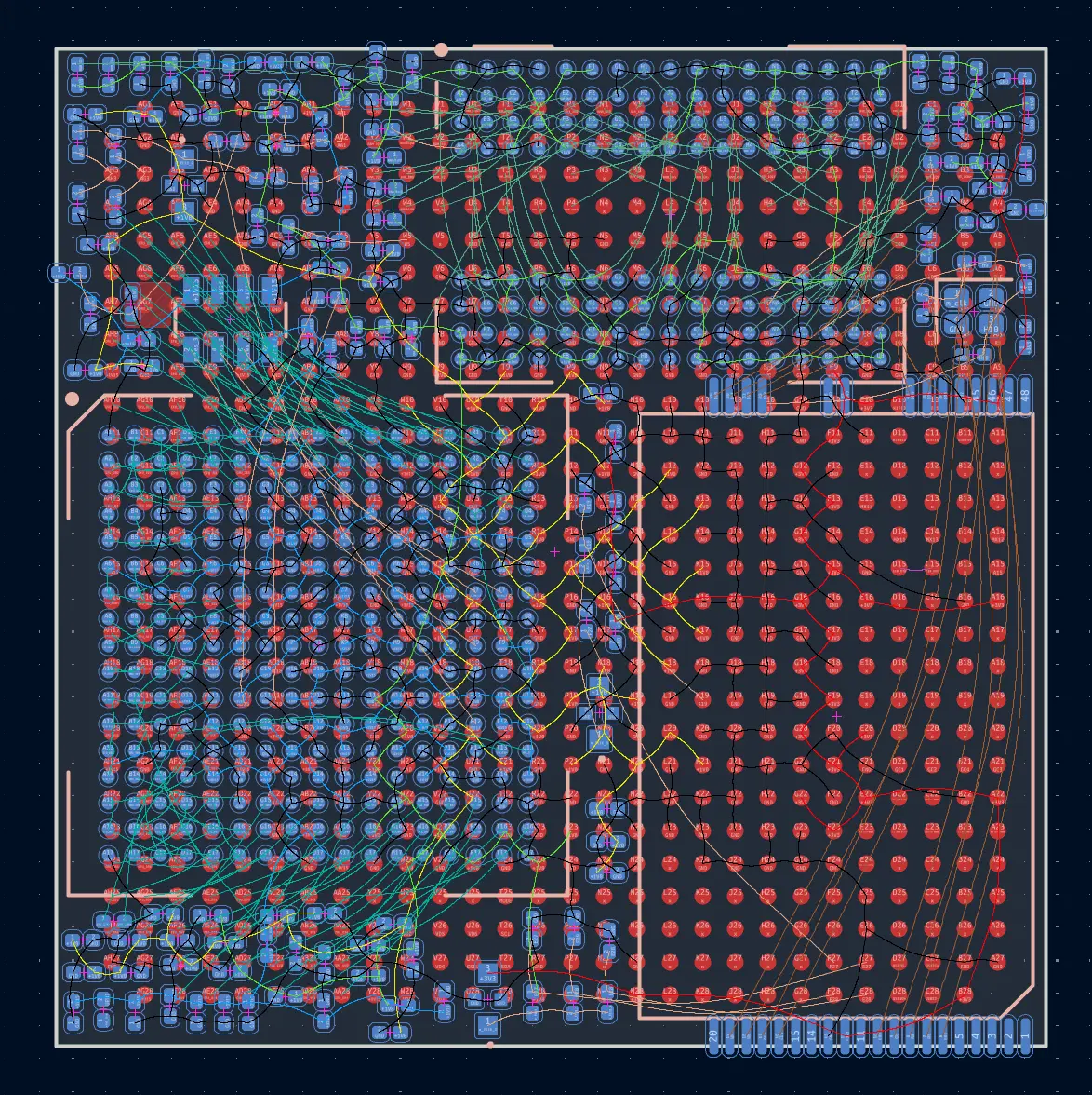
Though I’m not gonna make that any time soon. So, when I release the public version of the Pico, feel free to make the Wii Femto. Or whatever you decide to call it XP
GBAWii4 GBA shell
So, I’ve been working on the shell. The Fusion file is a complete mess, and I’m still not done, and am adjusting and printing and adjusting and printing… I’m trying to make the insertion of the Pico Pak work with the new riser after it arrived yesterday. And I’m trying to make the shoulder buttons work. And for it all to feel nice to hold and use. And I’m adding details which are too small to print…
I don’t feel like going through it in details as it’s still a work in frantic progress. So, here’s some images of it all
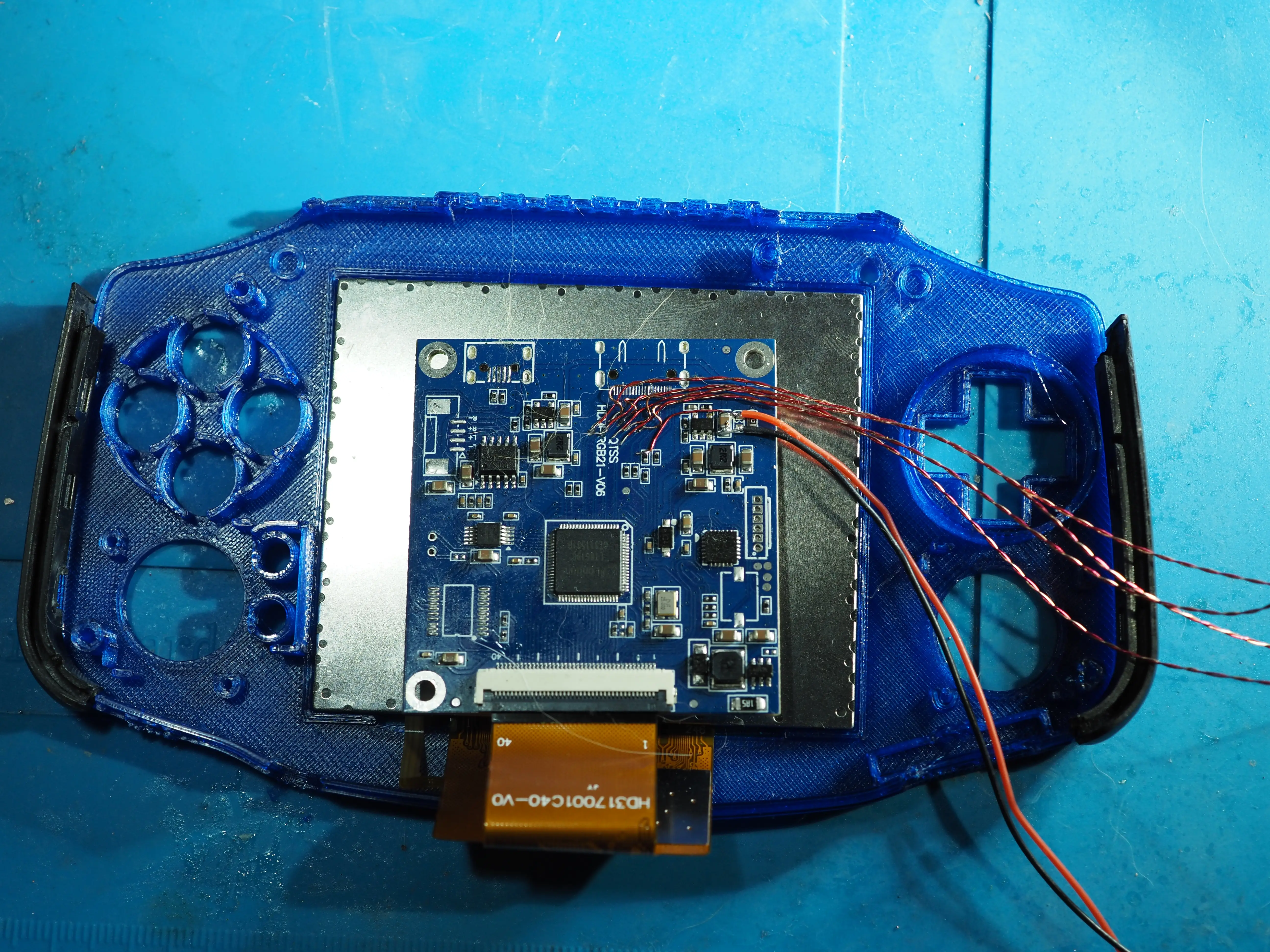
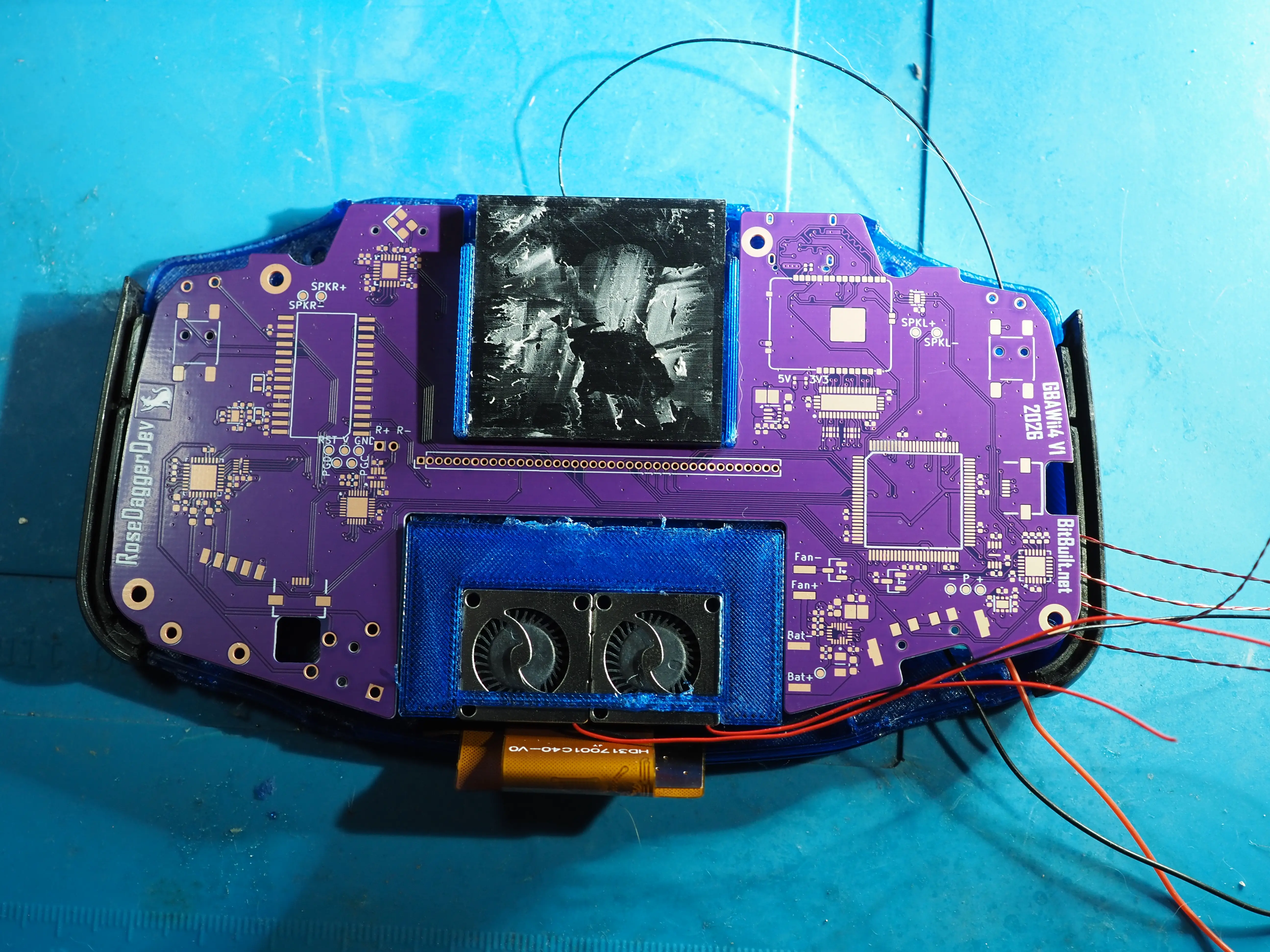
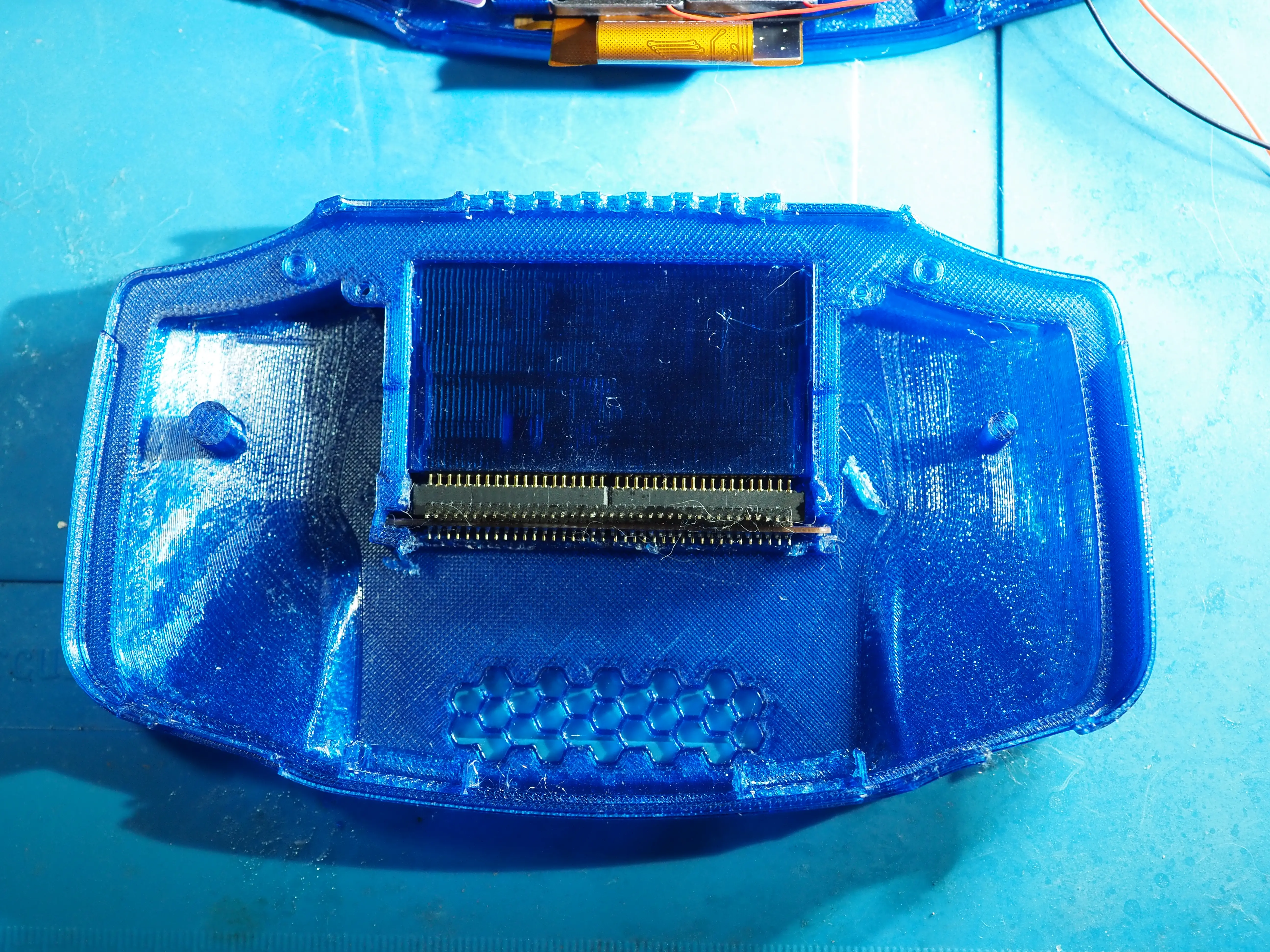
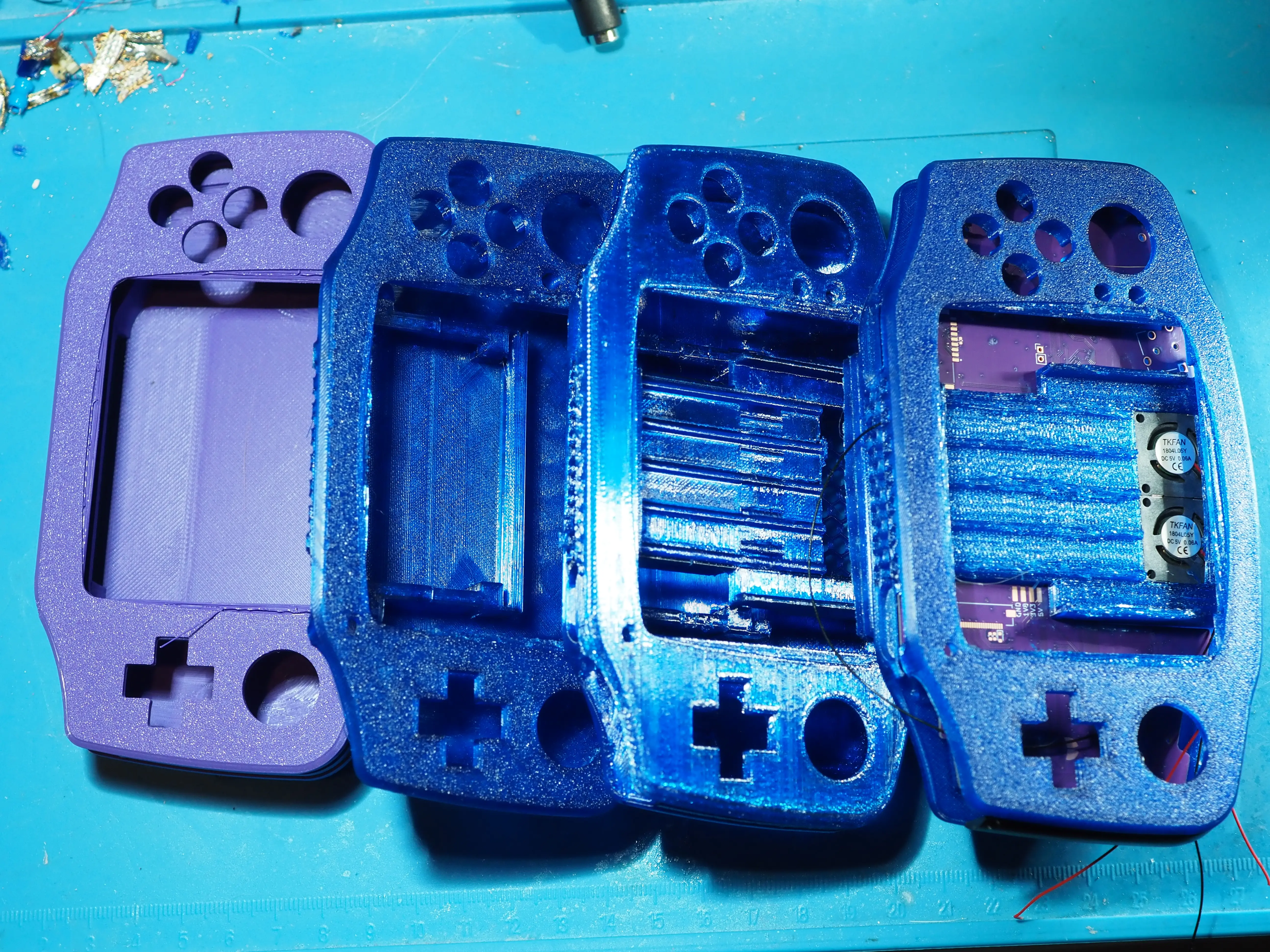
Rounding off the update
So where are we? And what is left?
I need the latest order of parts to come through. It got stuck in clearance, but it seems to be moving now. So, I should get the PIC for the GBAWii4 dock. And the parts for the Zero.
The Zero and riser arrived yesterday, and I soldered up the riser. Waiting on said parts for the Zero to solder and test it.
The Pico Pak is stuck in clearance currently, and I just got to hope that it goes through soon. It’s in my city, so it can be delivered as soon as DHL and the Irish customs agree that I’ve paid what I need to.
Then it is just finishing the case, putting everything together, and hope that it all works… I have one weekend left to do it. If the parts arrive, and I didn’t mess up anywhere else, then it should work. But if I mess up somewhere, or I break the screen last minute, or something else catastrophic, then I have no time to recover… So, it’s going to be down to the wire XP
And as soon as I’m done, I’ll need to work on my final year project for my EE bachelors, and spoiler, I’ll need to make a worklog here about what it will be XP
Anyway, that is me finally finished with my long-awaited update, and me signing off to be even more busy XP
First let’s have a look at how my plan from the last post went:
- Saturday 29th: Finish the GBAWii4 and send it to JLC for printing. 3-4 days manufacturing, and 2-4 days shipping, would mean I could get them as early as Friday this week if I’m lucky. (Complete)
- Sunday 30th: Finish the GBAWii4 if I didn’t on Saturday, If I finished, start on Monday’s task, allowing me to move the week plan up one day. (Failed, I was tired and played Stellaris the whole day instead XP )
- Monday 31st: Digikey components arrive, Bake Foxtrot and write the worklog (Complete)
- Tuesday 1st: Reball the HW2 and CPU, and prep for the Pico to arrive (Complete)
- Wednesday 2nd: Pico rev 2 arrives, solder all passives and small components (Complete)
- Thursday 3rd: Solder the HW2, CPU, RAM, NAND, and check resistances. (Complete)
- Friday 4th: If GBAWii4 arrives, solder it up. If not do finishing touches on the CAD for the Pico cartridge and send it off to be CNCed. (GBAWii4 did not arrive, worked on and sent the Pico Pak off to CNC) (Complete)
- Saturday 5th - Monday 7th: Test the Pico if the GBAWii4 dock arrived, or work on the CAD for the GBA shell. (Still no GBAWii4, Worked on the shell) (Complete)
- Monday 9th: GBAWii4 actually arrives, solder it up (Complete)
- Tuesday 8th: Uni starts up. (Complete)
- Debug and check the Pico and GBAWii4 works (90% complete)
- Write/modify firmware for the GBAWii4 (90% complete)
- Any last adjustments if needed (In progress)
- Get the Pico GBA cartridge CNCed (Waiting on delivery)
- Finish the design on the GBA shell (In progress)
- Get the shell resin printed in translucent purple if I have time (Ha nope no time)
- Print it at home if I don’t have time (In progress)
- Assemble everything (To be done)
- Final testing and showcase (To be done)
The next part is going to be multiple different sections as I worked on a lot of smaller issues over the last 3 weeks.
PICO Rev 2
I finished soldering it up during the week off I had and it looks amazing if I say so myself ^^
Now as for how to test it. It was still my week off, and I didn’t have the new dock… But I wanted to test if it worked… The old dock used a different pin spacing and connecting interface so I can’t just plug it into that now, can I?
Hmmmmmmmm… Even though the pinout changed the main features remain the same, what if I just solder some magnet wire on the video and power pins and hand wire the Pico Rev 2 to the old test dock? That should work, shouldn’t it?
Hmm that worked surprisingly well! Now let’s see if it boots?
Do I get power? Check!
Does the GPU and CPU heat up? No…
Do I see any reasonable activity on the data or clock lines? Nope…
Let’s check U10 reset? 2.3V… What?
Okey I know what’s going on here, and I’ll explain.
So while changing the ThunderVolt source code to work with the PicoThunder (aka my implementation of the ThunderVolt on the Pico). I discovered that there was an option to emulate U10 without using a MOSFET. It would instead wire the reset line directly into a pin on the Tiny, then it could pull the pin low to reset, and set the pin to high impedance to let the GPU pull the line up to 3.3V. It seemed brilliant, I loved it, and since the MOSFET on the Rev 1 had been one of the things I failed to solder initially, it would remove a potential fault source. So of course, I removed the MOSFET for Rev 2 and used this emulated U10. However, there was one aspect that I had not considered. The Tiny runs on 1.8V, the reset line is 3.3V, the voltage protection on the Tiny is VDD + 0.5V. 1.8V + 0.5V is for those who are good at math, less than 3.3V. It’s 2.3V to be exact…
Now this is a tiny little bit of an issue, as 2.3V is apparently not enough for the GPU to go out of reset…
The obvious solution is to place the MOSFET back. Don’t fix something which isn’t broken. However I had removed the footprint completely, so my other option was to cut the trace, solder some magnet wire to the traces, and solder on a MOSFET. The trace width is 0.1mm, my magnet wire is 0.25mm in diameter, the MOSFETs I had in my backup pile is a tiny 1x0.6mm MOSFET with tiny pads… Yeah no I don’t feel like soldering that XP
(Now that I think on it, I could have used the U10 MOSFET from the Wii, that would have been easier to solder, but I didn't think of that at the time.)
Now the other option was to increase the VDD on the Tiny. The voltage comes for a small LDO which uses a resistor divider to set the output voltage. The 1.8V is only to make it use less power, while the tiny is fully capable of going higher. Checking my book of 0402 resistors, I can make the LDO output 3.04V. 3.04V + 0.5V is in fact greater than 3.3V. I could have gone a bit lower, but it would mean replacing both resistors, and this worked, so (shrug). It will use a little bit more power, but it should be fine, everything else connected to it is 3.3V tolerant so it does not really matter.
For the public release I’ll put the MOSFET back, and call it Rev 2.1. XP
Now does it boot? Nope, it does not seem to be able to maintain the main clock. Last time I replaced the caps on the main crystal. But didn’t this time. A quick swap of load caps and the clock is running. I’ll fix that for the public release as well.
Does it boot now? Ish… It clocks are running, it heats up, but the video clock is 27MHz… I’ve seen that before, so I poke each leg on the NAND to see if they are soldered. Don’t see any of the legs moving… I measure again… 54MHz! I connect the monitor, and behold:
It seems of all components on the PICO, it’s the NAND I struggle with the most XP
But I’ve proven that the Pico Rev 2 works and only needs some minor fixes which I don’t need a new print for. Whoop!!!!
Pico Pak
Did you know the official name for the Gameboy cartridge is Gameboy Game Pak? As such I named the cartridge for the Pico, the Pico Pak.
Now I had done most/all the design a lot earlier, I just wanted to measure the final Pico to be triple sure the dimensions would be correct, then go over and round all edges.
I had fought for every fraction of a millimetre of space in the height direction, so that the GBA connector would fit, even delided the chips just to get slightly more clearance. And I had cut into the top and bottom to the maximum thin wall limitations for JLC.
I had also made this really cool locking mechanism, where the two pieces would slide together and the hooks would interact with the pegs. Locking it in all directions, and the screws were only needed to make sure it would not slide apart. And it worked well 3D printed!
So with all finishing touches done, I sent it off to JLC for CNCing to see if they could machine it.
Nope. They didn’t like the pegs at they could not give me undercuts. And they didn’t like that all wall thicknesses were in the “thin wall” range. Apparently, you needed some normal walls to provide enough support or something XP They wanted the main top/bottom surfaces to be 1.5mm thick at least… They were 1mm thick with some parts recessed to 0.8mm… All my efforts to gain every bit of height were wasted. And the GBA connector would never have fit XP Good thing I had switched to the pogo pins, right?
Shit… I’m getting squeezed and it does not fit… Fuuuuuuuuuuuck… I ask JLC if they will allow some cutouts in the main surfaces below 1.5mm as long as most of it is 1.5mm? And they answer that yes that is allowed. Okey cool, maybe I can save this? What if I flip the connector around to the top? There it would have more space…
Yeah, that would work! Hallelujah, the main design will still work!!! It would cover up the AGB-RVL-02, but that is fine. Though there was a second issue… All these changes would of course mess up the height of the riser for the meeting pogo springs. But that is a cheap 2-layer board, so I can have that reprinted. But it means I can’t test the Pico with the new dock when it arrives… But oh well, I already know that it works due to testing it with the old dock.
Now over to the second issue… No undercuts… My hooks and pegs won’t work… But I want some more support than just the screws… Guess I’ll just make some tabs which goes down and meets surfaces on the other side, locking it in all directions except straight on? And then the screws hold it in in that direction?
Well that seems to work!
Now… Since I was already changing the design… I figured maybe I’d add some more details? I had added the Wii Pico as a raised section in the area where the GBA game label was supposed to be. Mostly due to that cutting the letters into the area where Gameboy Advance is supposed to be, would have been too small for the cutting bit. And I didn’t know how to make a technical drawing for lasering. But to tap my screw holes I needed to learn to make a technical drawing… So why not laser? XP
Now it was fully done, so I sent it back to JLC, and they approved it! Whoop!
GBAWii4
Now onto the GBA dock, I got the PCB back and soldered it up without too much hassle.
Some firmware writing later, and I could control the RGB light, the 5v regulator for the display. (I can very likely run the display of 3.3V and 1.8V, but I don’t have time to check). The power switch for power to the PICO. And the charging controller. One tiny note, apparently the “Absolute input voltage regulation limit” is the absolute minimum voltage, not the absolute maximum voltage… I set it to 16V and then ended up confused why it never tried to charge the battery. Changing it to 4V and suddenly it was happy to charge XP
The only bits left to test requires that the Pico is inserted. The dock feeds battery voltage into the Pico, and the Pico feeds 3.3V and 1.8V back out using the regulators on it. So, anything connected to 3.3V and 1.8V requires the Pico.
Well, there is one thing I can do while I wait. I can program the PIC for GC2+. I connect it up to the programmer, and try to program it… MPLab is throwing some errors… It is expecting a PIC18F25K42, but I have a PIC18F24K42… That’s odd, but surely, it’s not a big deal, I’ll just update the targets in MPLab and flash it… Now it is complaining that it does not have enough space… The F25 has twice the space of the F24… And GC2+ uses most of that space… Yeah no I’m not fitting it on my PIC… Why do I have the wrong PIC? I copied it from my previous design for last year’s contest… Let me check the source schematic for the GC2+… It needs the F25… I have no clue why I picked the F24… I did it last year and never reached the bring up stage to notice the issue. But oh well. I have the GC2+ from 4-layer tech from when I did my first contest entry in 2021. Maybe I can just use the PIC from there? Nope it’s the wrong size… I got to order the correct one… Oh well there’s enough time at the point I discovered the issue. Good thing I tried it when I did XP Now let’s just hope there’s no other issues as I won’t have time to fix them…
Wii Zero
One night I lay thinking about the title for the smallest Wii in the world. The Pico in the Pico Pak would be the smallest Wii motherboard, in the same way that the Kawaii is the previous smallest. But both require a dock… And I have more stuff in the dock… So my claim to be the smallest always comes with an asterisk… The TV dock was supposed to fix that, but I abandoned it… But maybe I could unabandon it?
I took a look at the test dock… It’s very sparsely populated, and about the same size as the Pico Rev 1. I have the Pico Rev 1 still laying around and it works. The main issue was the connector and the 3.3V regulator… What if I quickly made a new dock for it, which I could hard solder the Pico Rev 1 to? It would not be in a GBA Pak, but it would let me stack the PCBs. And if I feed 3.3V into VDD on the Pico, then I can remove the 3.3V regulator completely and just solder a jumper between VDD and 3.3V.
So, I got up and made an ultra-quick mock-up. Using the footprint of the Pico Rev 1 as my max PCB size, and tried to see what I could fit in.
So, this fits inside the bounds of the Rev 1, and it is GCVideo, straight into MelonHD. For USB C DP out. It gets PD in and feeds it through a 3.3V regulator. It uses WavePhoenix for controllers, and the Bluetooth module for Wii motes. And the GL827 for SD to USB. The only ports on it are the USB C for power and video out, and the SD card slot. And it all took about 24h from I thought of it, till I was ready to order XP It’s mostly just reusing parts from different projects and then playing Tetris for a few hours.
Now why did I do this when I’m already swamped with stuff to do? I wanted to fully claim the title for the smallest Wii in the world without any asterisk or caveats. The Kawaii, the smallest Wii which requires a dock is 60x60x15.8mm. This Wii Zero, would be just 52x36x7.2mm! Sure, I would need a case and a heatsink, but I would still, without any question be the smallest Wii in the world! And that was kinda the point of making my own PCB and moving the RAM around to the backside.
The Pico Rev 2 will be the smallest Wii motherboard which requires a dock. While the Wii Zero will be the smallest self-enclosed Wii in the world! Yes, I’m greedy and want to steal all the titles XP
Can we go smaller?
There was a small discussion in the discord about JLC adding HDI vias, aka buried and blind vias.
And if it was possible to make the Pico even smaller… So of course, I made another ultra quick mock-up XP This is the CPU also flipped around to the back. And all passives as 0201. It all fits within the footprint of the GPU XP It would be hell to trace it all and would need to use HDI which would be even more expensive than what I’ve done so far. But it is technically possible to fit it all. Will it work (shrug) all the passives would be in the wrong spots, and all traces, lengths, and impedance would be off. But maybe. I proved that it worked for the RAM, and that is higher speed than the CPU.
Though I’m not gonna make that any time soon. So, when I release the public version of the Pico, feel free to make the Wii Femto. Or whatever you decide to call it XP
GBAWii4 GBA shell
So, I’ve been working on the shell. The Fusion file is a complete mess, and I’m still not done, and am adjusting and printing and adjusting and printing… I’m trying to make the insertion of the Pico Pak work with the new riser after it arrived yesterday. And I’m trying to make the shoulder buttons work. And for it all to feel nice to hold and use. And I’m adding details which are too small to print…
I don’t feel like going through it in details as it’s still a work in frantic progress. So, here’s some images of it all
Rounding off the update
So where are we? And what is left?
I need the latest order of parts to come through. It got stuck in clearance, but it seems to be moving now. So, I should get the PIC for the GBAWii4 dock. And the parts for the Zero.
The Zero and riser arrived yesterday, and I soldered up the riser. Waiting on said parts for the Zero to solder and test it.
The Pico Pak is stuck in clearance currently, and I just got to hope that it goes through soon. It’s in my city, so it can be delivered as soon as DHL and the Irish customs agree that I’ve paid what I need to.
Then it is just finishing the case, putting everything together, and hope that it all works… I have one weekend left to do it. If the parts arrive, and I didn’t mess up anywhere else, then it should work. But if I mess up somewhere, or I break the screen last minute, or something else catastrophic, then I have no time to recover… So, it’s going to be down to the wire XP
And as soon as I’m done, I’ll need to work on my final year project for my EE bachelors, and spoiler, I’ll need to make a worklog here about what it will be XP
Anyway, that is me finally finished with my long-awaited update, and me signing off to be even more busy XP
- Joined
- Jan 15, 2021
- Messages
- 68
- Likes
- 267
- Portables
- Wii PICO (Complete), Wii Zero (WIP), GBAWii4 (WIP), GB Adwiince v3 Revenge (On Hold), GB Adwiince v2 (Dead)
Final upload videos. Didn't get done, but here is where I ended.
Edit 1: These were shot at 5am, after an all-nighter with 15min left before the end. So they might not be great XP
I'll write a proper end worklog later of everything that happened
Edit 2: I'll include the goals set out in the beginning and which ones are cleared
Main goals:
Edit 1: These were shot at 5am, after an all-nighter with 15min left before the end. So they might not be great XP
I'll write a proper end worklog later of everything that happened
Edit 2: I'll include the goals set out in the beginning and which ones are cleared
Main goals:
- Fully redesigned Wii motherboard with transplanted CPU, GPU, RAM and NAND. (COMPLETE)
- Putting the redesigned Wii into a GBA cart. (COMPLETE)
- Create a simple dock to test that the redesign worked. (COMPLETE)
- Create a handheld dock in the shape of a GBA. (90% Final fixes and assembly missing)
- Create a TV dock, which should hopefully be the smallest Wii ever made (so far). (80% Need to fix a bug, and create a case for it)
- Actually, having something work at competition end for once. XP (Eh, the Pico worked, but a final console using it was not complete)
- GBAWii4: MX, GCVideo, MelonHD, MIPI display and redesigned driver board. (90% Done, to everything except MIPI which was changed for HDMI)
- TV Dock: MX, Bluetooth, AVE/component out, sensor bar plug, 4 GC controller ports. (80% Done, this became the Zero, which has WavePhoenix, BT, USB C DP out)
Last edited:
- Joined
- Jan 15, 2021
- Messages
- 68
- Likes
- 267
- Portables
- Wii PICO (Complete), Wii Zero (WIP), GBAWii4 (WIP), GB Adwiince v3 Revenge (On Hold), GB Adwiince v2 (Dead)
Heya, so I’ve been wanting to make a proper update for what happened in that last week. Though do note that competition is over and it’s the stuff before this update which counts.
Before the final weekend
After the last proper update, I got a message from DHL that the Pico Pak was taken for clearance, and that I needed to supply proof of purchase. I did so, and the Pico Pak was released shortly after and arrived before the weekend
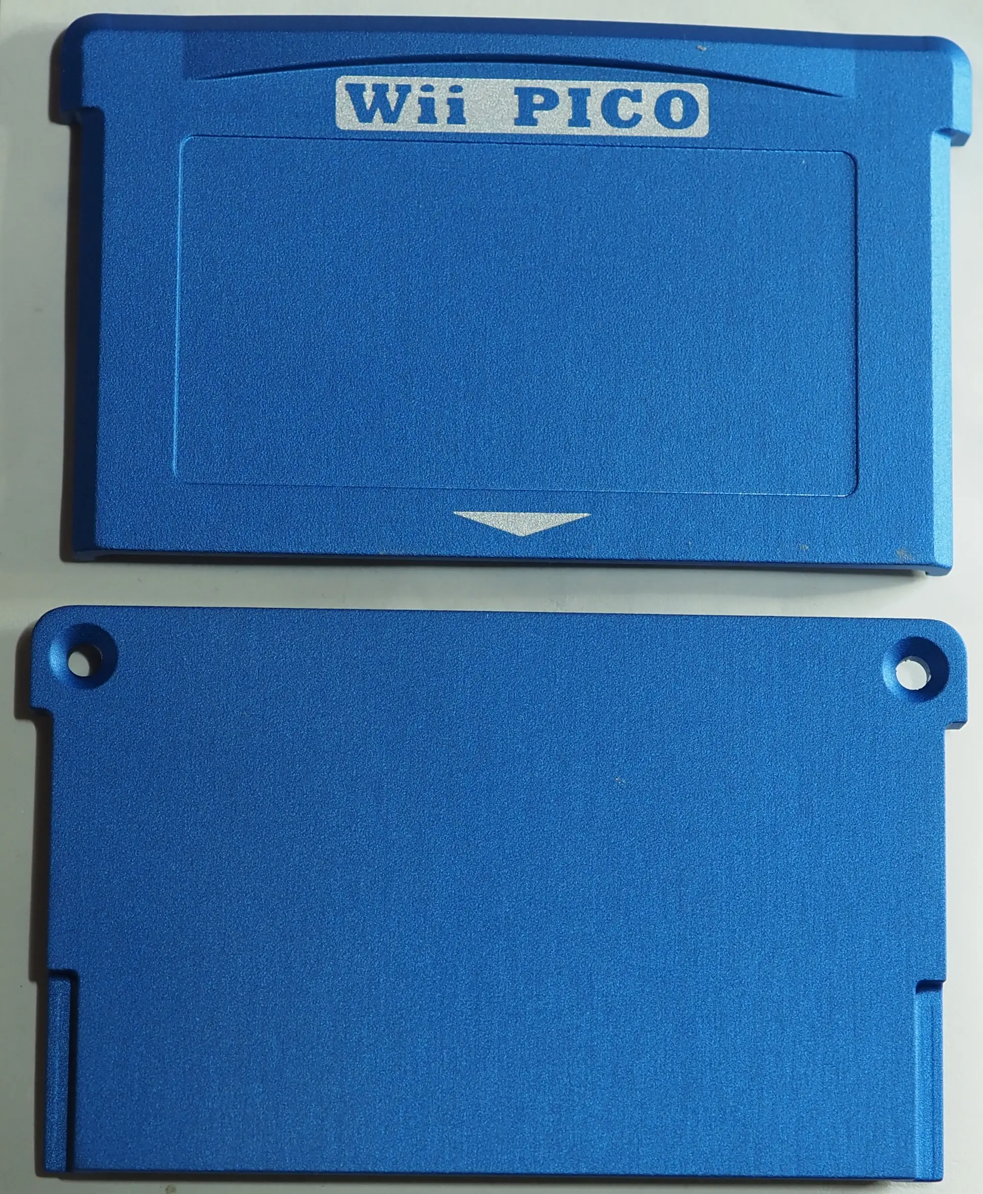
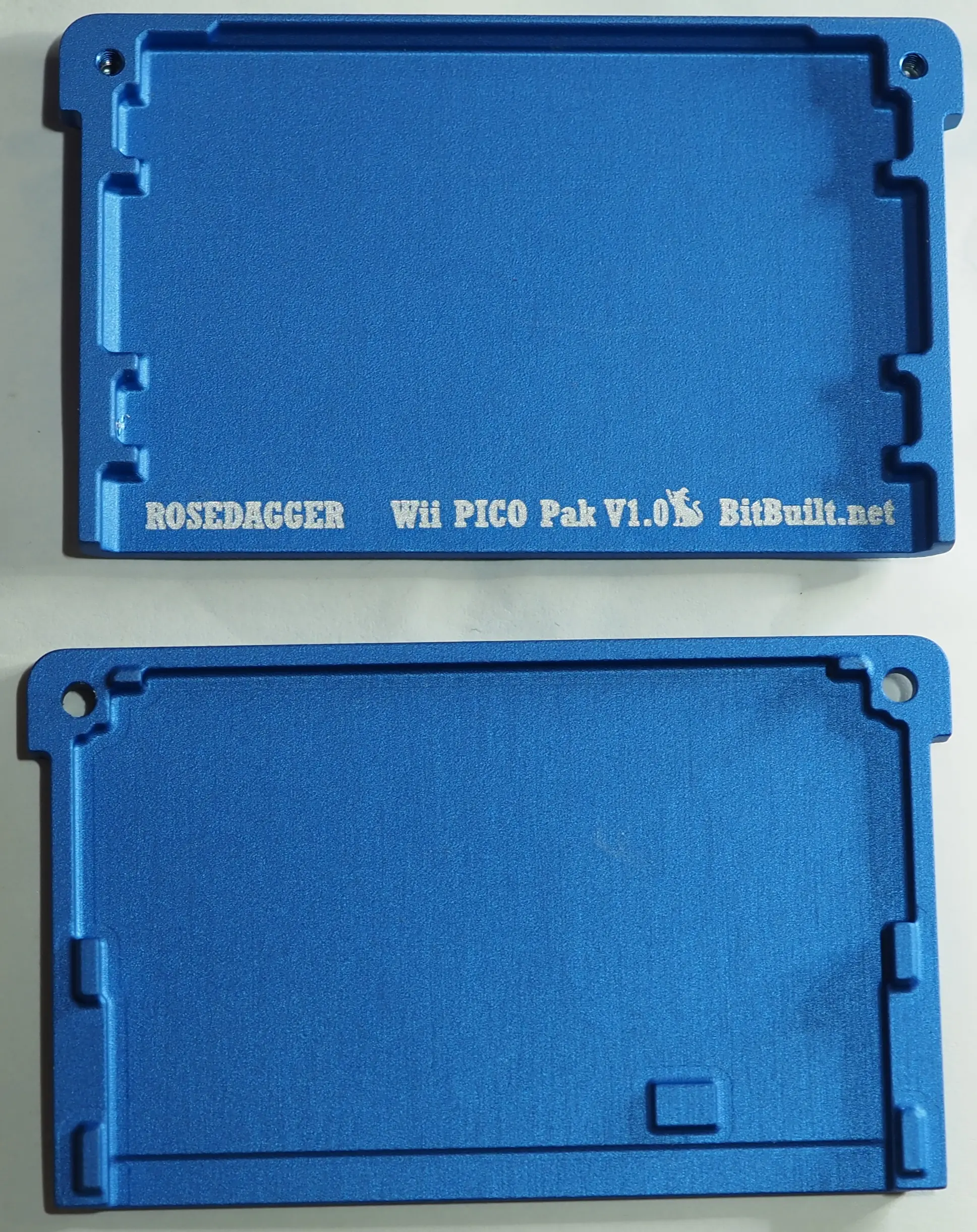
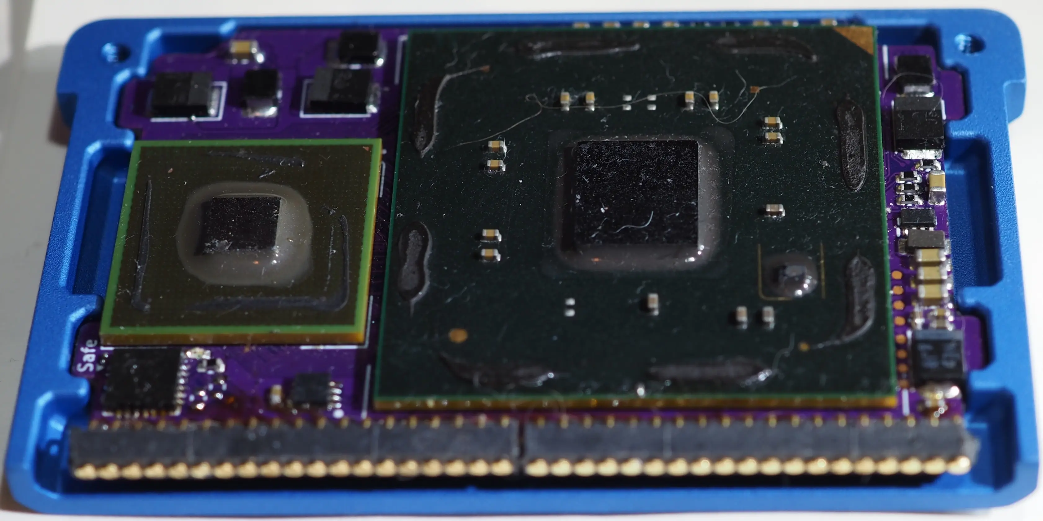
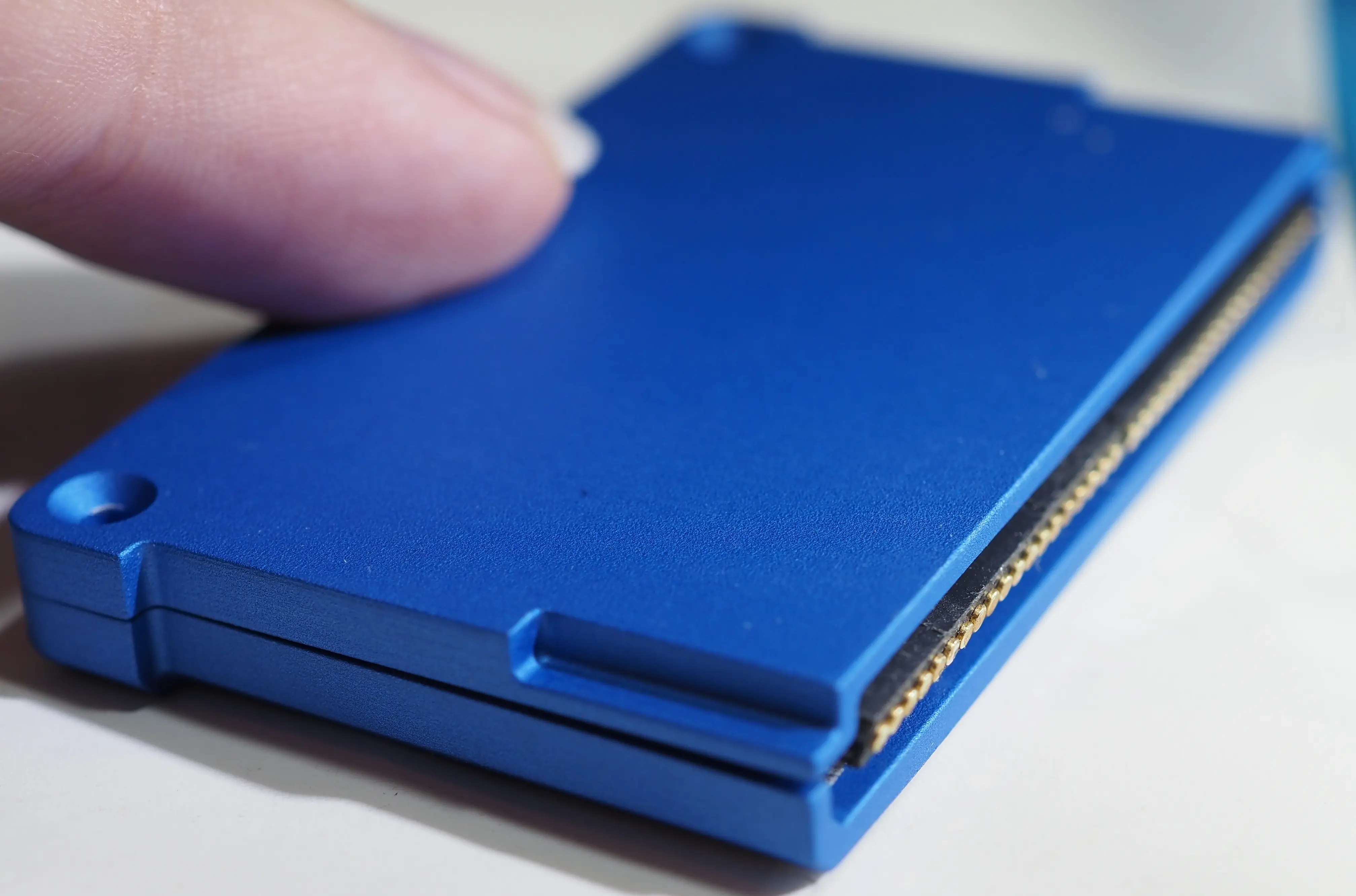
I love it, it fits together so well ^^ However there is one minor issue… It does not want to fully close with the Pico inserted… As it turned out, when JLC asked me to thicken the case, I moved the Z position of the Pico, but I forgot to check all clearances… And the ram now collides with this ledge
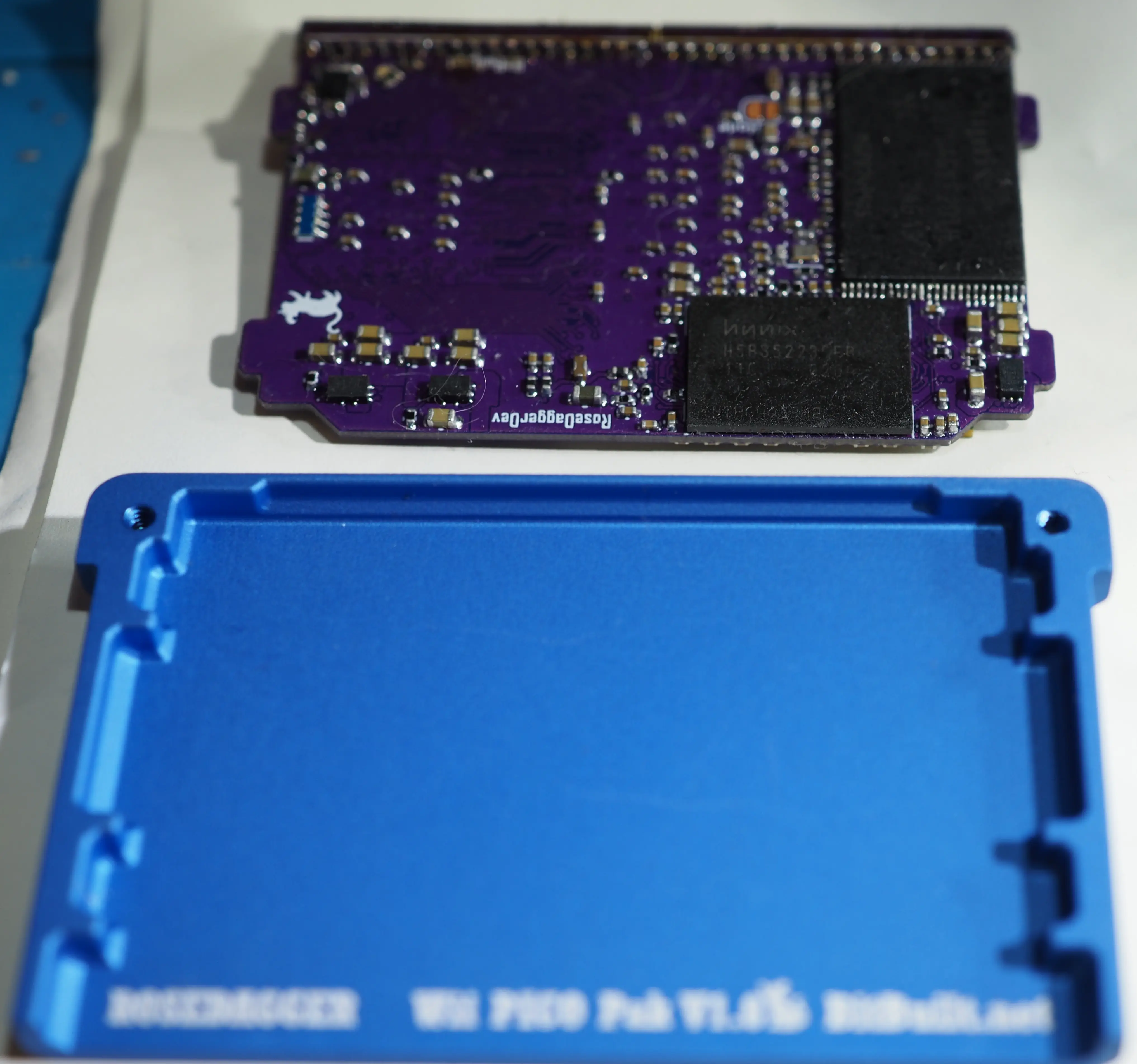
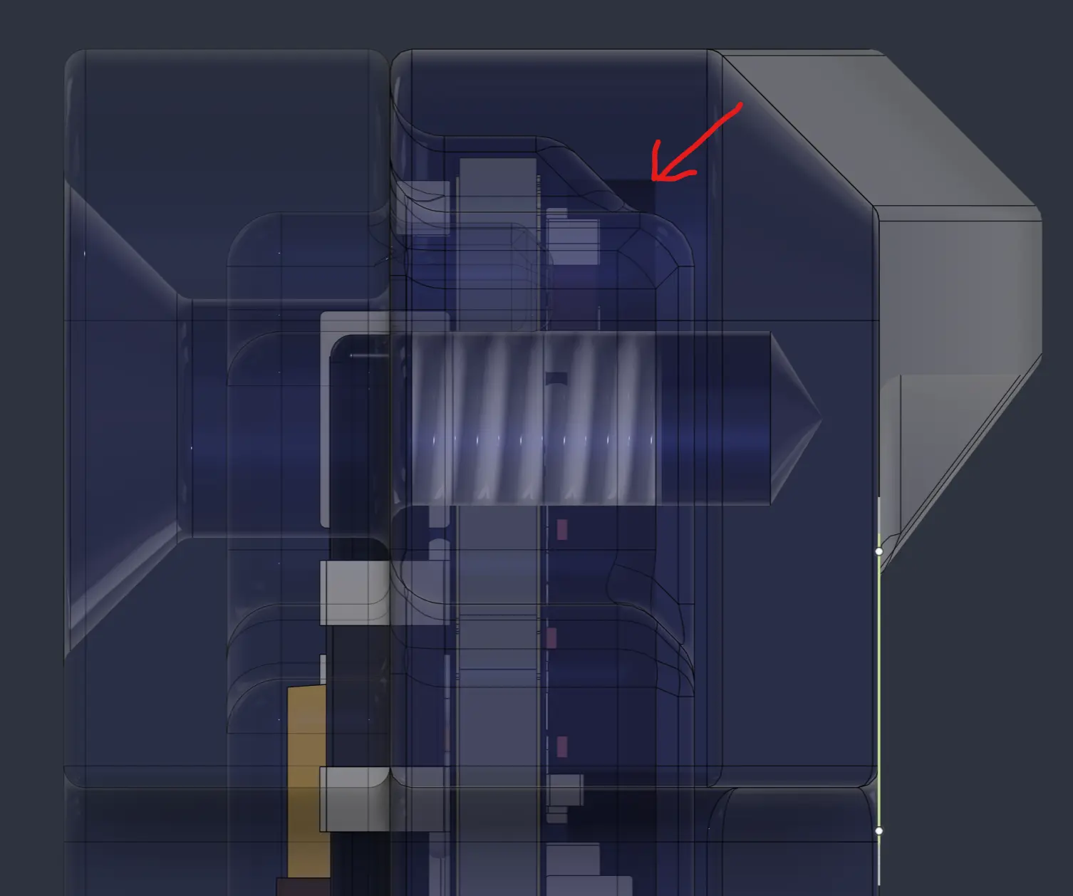
So, I grinded it away XP After which it closed as expected!
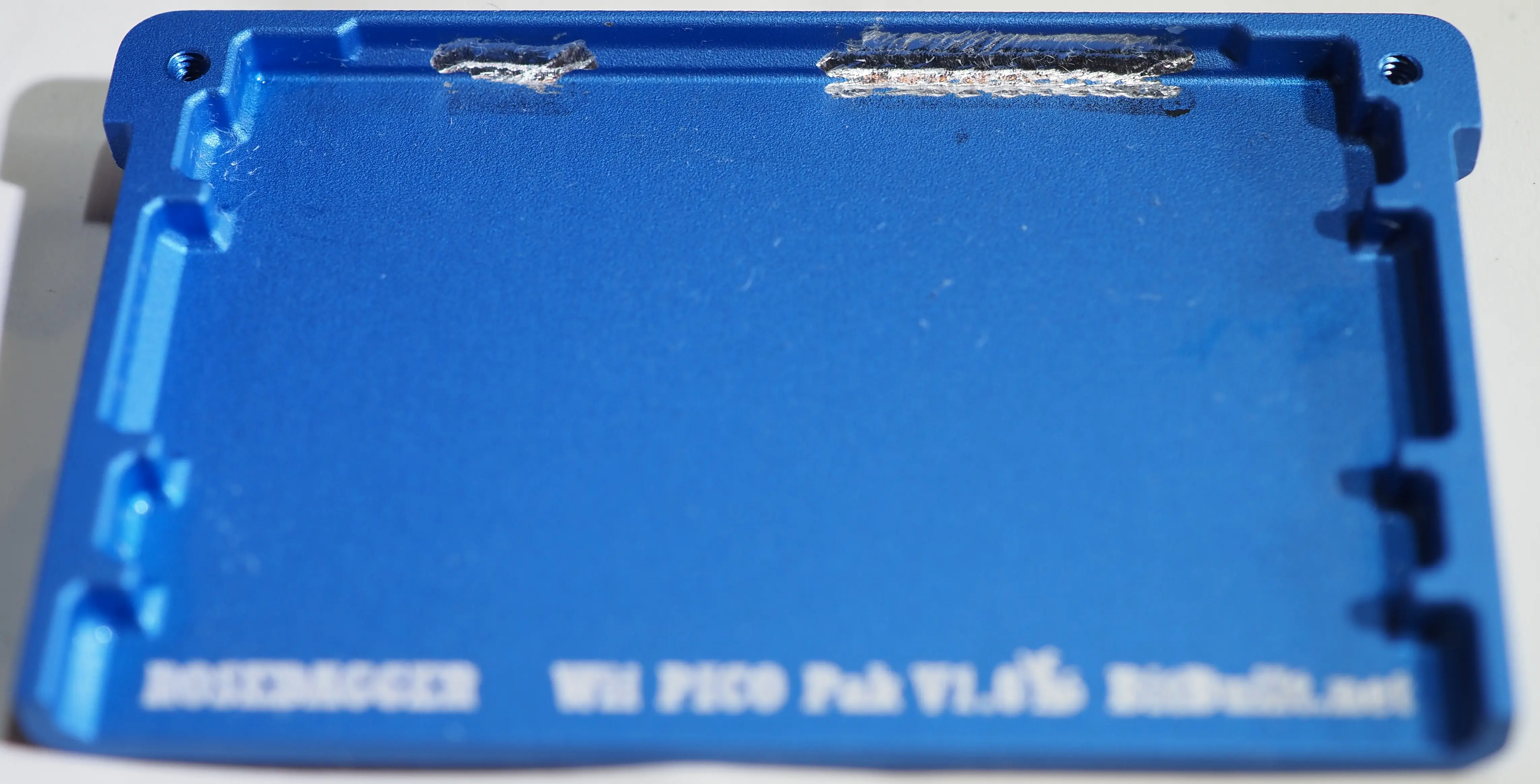
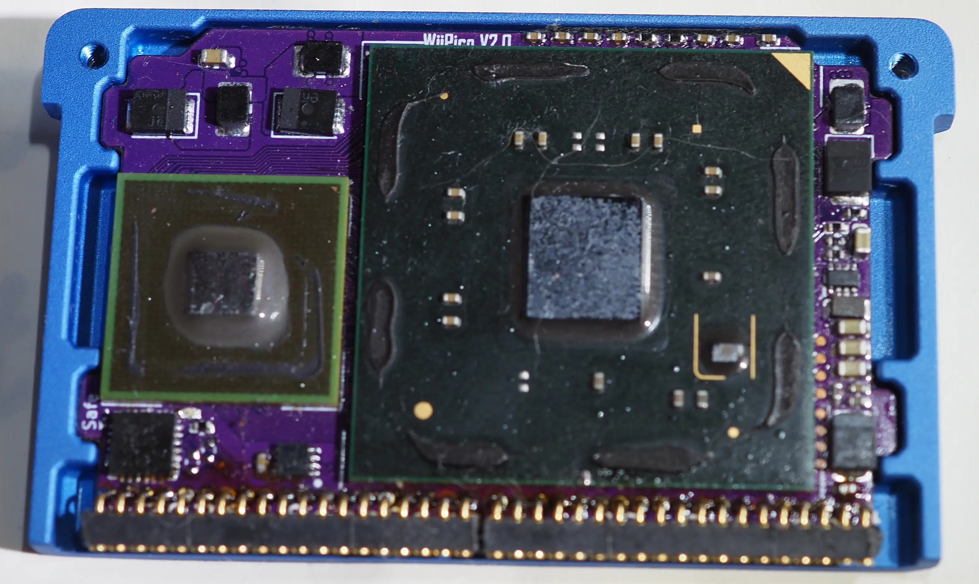
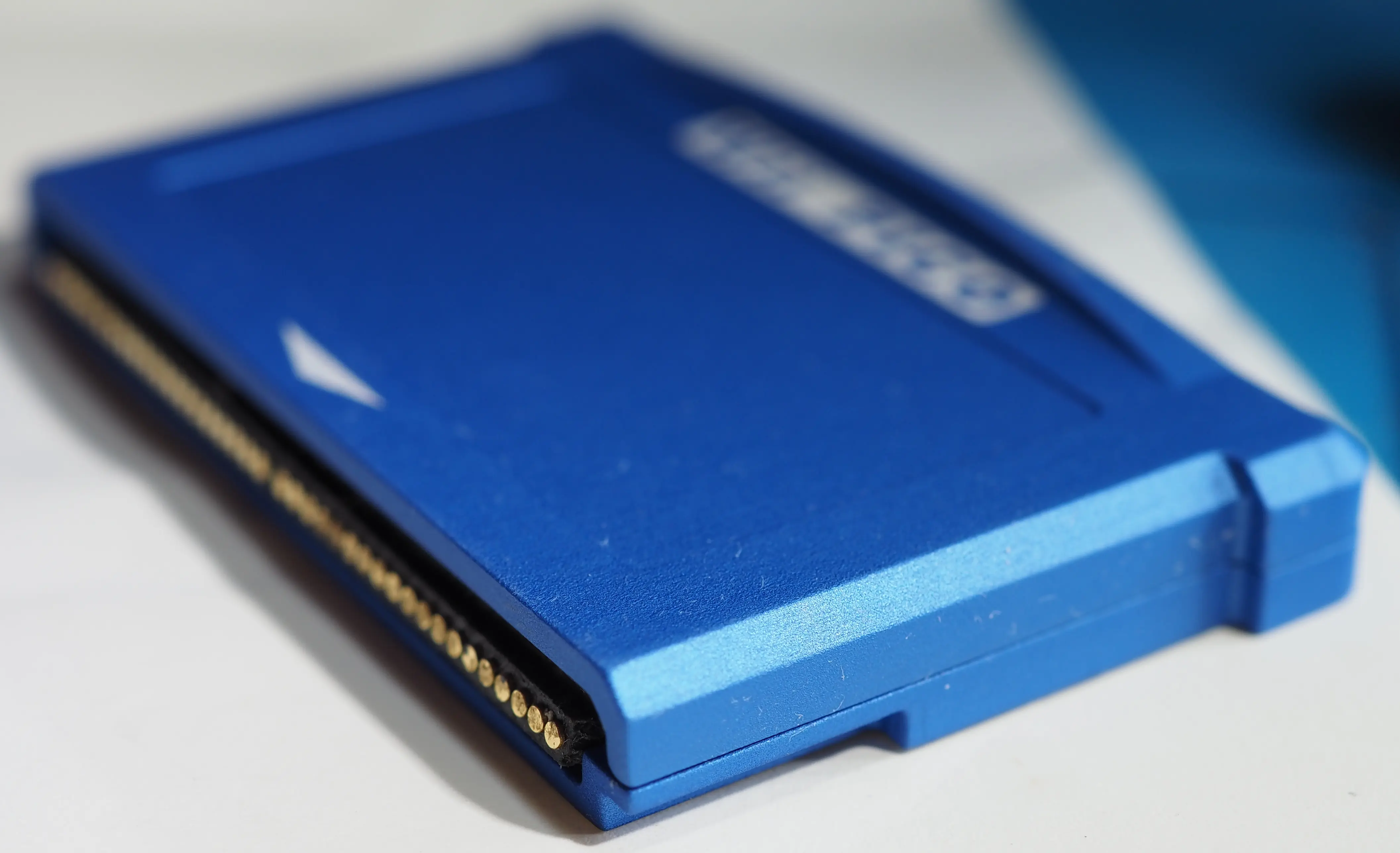
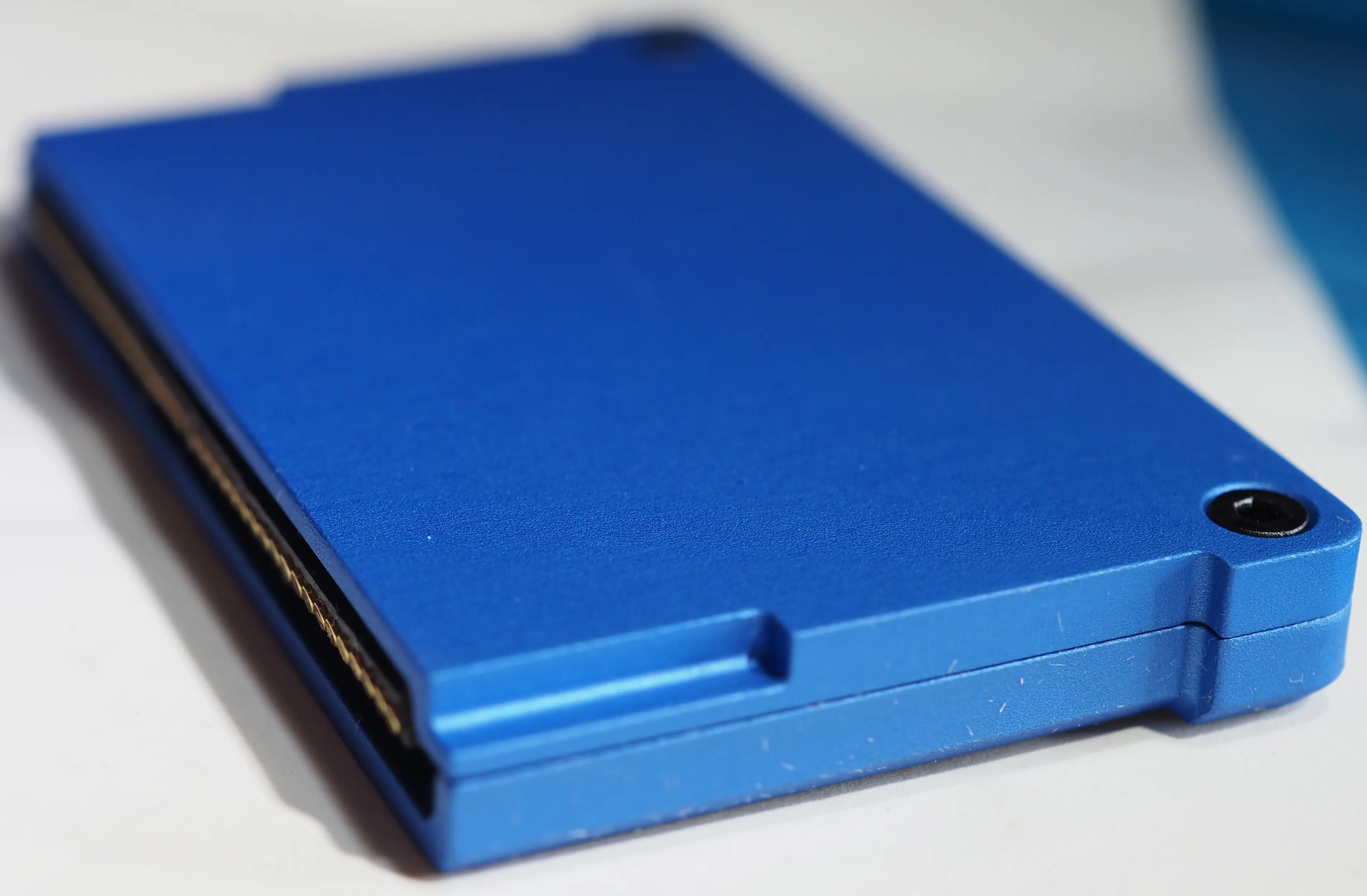
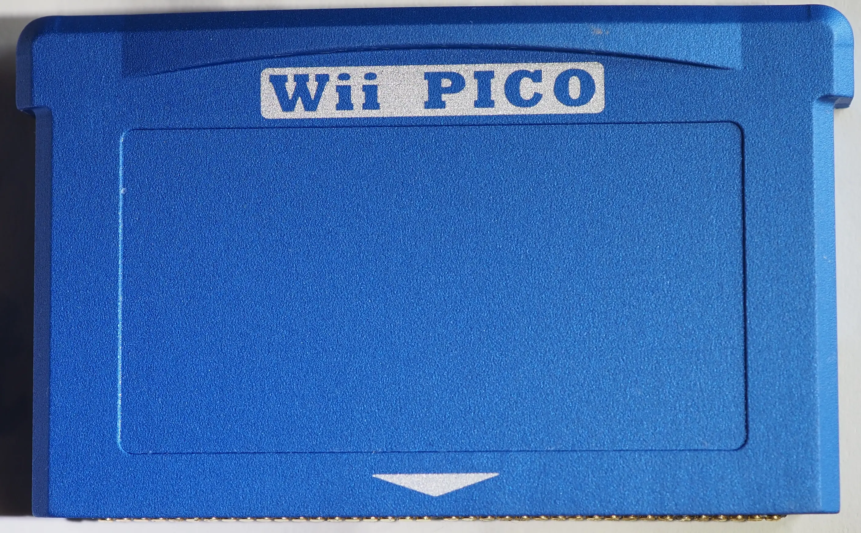
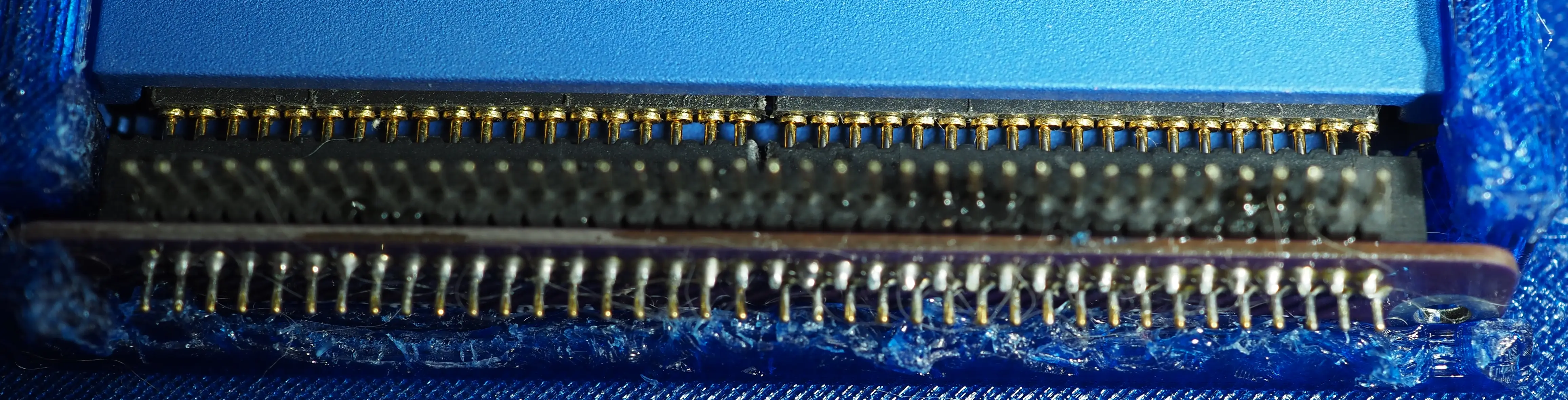
Now there was another few packages I were waiting on, including the package from Mouser, which contained the parts for the Zero, and the correct PIC for GC+ 2.0. I had ordered the components on September 14th, which should have been plenty of time… Right?...
The components arrived in Ireland on Wednesday the 16th but got held up by clearance.
On Monday the 21st the components left Shannon distribution centre. Yey it’s moving!
On Tuesday the 22nd the components left Shannon distribution centre. Hmm the previous one must have been a mistake.
On Wednesday the 23rd I got a call from FedEx saying my package containing *checks notes* “Ceramic capacitors?” was held up by clearance, and that I needed to supply proof of purchase.
On Thursday the 24th the components left Shannon distribution centre… I have a bad feeling about this…
I email them again, I need the components ASAP preferably before the weekend, but hear nothing…
On Friday the 25th the components left Shannon distribution centre… Oh no…
I went through Ask FedEx chat support and supplied the proof of purchase there as well… And a few hours later I hear back! The package has been cleared!!!
On Monday the 28th the components left Shannon distribution centre… Fuck!
On Monday the 28th the components arrived at the local FexEx facility! Wait it moved!
On Monday the 28th the components left on a FedEx vehicle for delivery!! It’s actually going for delivery!
On Monday the 28th the components arrived at my house!!! I’m out of purgatory!!!
I had 3 days to solder and test everything… Where did all that buffer time go? XP
I had one more package mishap, I ordered a Wavebird controller to use with the Zero. I ordered it on September 12th, it was supposed to arrive between September 22nd and October 2nd.
… And arrived at my place on October 5th… What the fuck is up with shipping?!
The final weekend, and 3D printer adventures…
It’s the final Friday, Friday the 25th. It’s the final weekend and I still have quite a few things to do. But with a full weekend I should have plenty of time. So, this was the basic plan of what was left:
It seems like a lot, but it should be doable as long as nothing goes too wrong… I have the whole weekend, and a short day on Wednesday, and I could always pull an all nighter if I need that last push. Though I’m to feel a bit iffy… But it’s fine, it’s just a cold, I’ll power through.
So on that Friday I did some more case work. And one package which did arrive was an Aliexpress order, which contained my new 0.2mm nozzle, which would allow me to do higher quality final prints!
I look up the instructions for changing the nozzle on my new K2 Pro. Unscrew the 0.4mm nozzle. And start screwing in the new nozzle. Hmmm, should it be that hard to tighten?... Let me unscrew it to check that I’m not cross threading the threads… Oh… Only half of the nozzle came back out… Well, that sucks… But if I screw it in again, it should line up and still work? Right? Getting the other piece out will be a future me problem… I tighten the nozzle again, but it gets fully stuck… But it has auto levelling based on the nozzle, and it’s just the final bit which didn’t go all the way in… Maybe it will work?
So, I turn on the printer, and make it extrude the filament… *Clunk* Oh the nozzle collides with the poop chute… Yeah no this is not good… Emergency shut down… And now it’s time to look up how to disassemble the whole hot end… yey, extra stuff I need to do…
Some disassembly later, and I have the piece which is stuck in the heat break… It’s really stuck and no amount of pliers can get it out… In the end I needed to do some percussive maintenance…
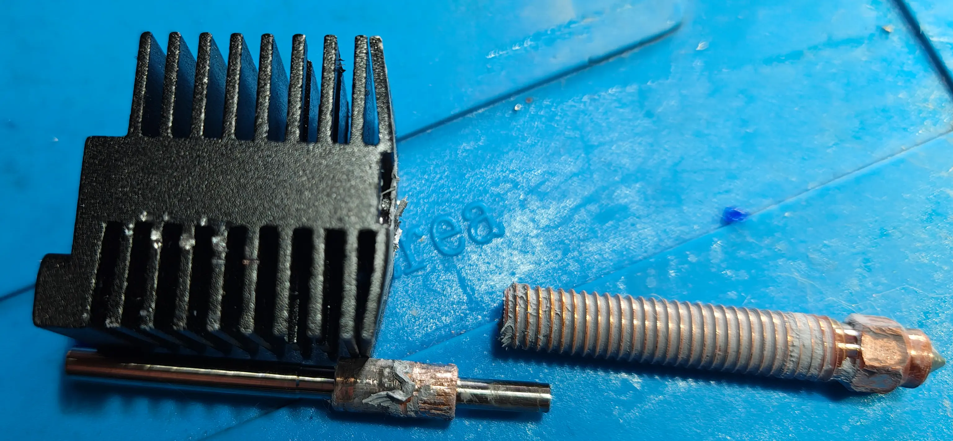
Note to self, don’t buy cheap nozzles from Aliexpress… The stock Creality nozzle is 4.75mm in diameter, the Ali special was 4.8 - 4.85mm making it just slightly to big to fit…
Also note to self, when something feels wrong. STOP, and don’t continue…
Anyway, I ordered an official Creality 0.2mm nozzle with next day delivery, and managed to fix the printer XP
Saturday, Sunday and Monday?
What had only been a cold on Friday, turned a lot worse on Saturday… It felt like a fever… But I still had stuff I needed to do! So, chugging some paracetamol, I tried to power through like planned. I can be sick later; this is more important!
First, I did some accounting, I had wanted to know how much this whole project had cost me, so I made a little spreadsheet. Note that the categories are a fluid, and there are parts which are under one category which are used other places as well. And the Shipping and Tax section is primarily for big ticket items like JLC and Digikey/Mouser. Smaller items from Aliexpress and Amazon has their shipping and tax included in their items.

So, I’ve spent about 1700€ on this project! Which is ~1900$, or ~1440£. So yeah, it’s not cheap XP
After procrastinating I needed to return to actually working on the project, though my headache and being generally properly sick had not gone away… It had actually gotten worse…
I took out the GBAWii4, slotted in the riser, then tried to boot it… Why is it not turning on?... I poke it with a multimeter, and it has power… I connect over UART… Nothing… Hmm, that’s odd, it was working a few weeks ago when I programmed it initially. But oh well, I’ll just reflash it and see what debug stuff I can add. Hmmm… The programmer can’t talk to the Tiny… Fuck, is it dead?!
I look around and find that I have one spare Tiny that is not being used. So I desolder the old one, and solder on the new one. And I can talk to it with the programmer! Yes! Oki lets see if it will run… No… Out with the multimeter… There is a short on SDA and none of the pins on Port B is reacting at all…
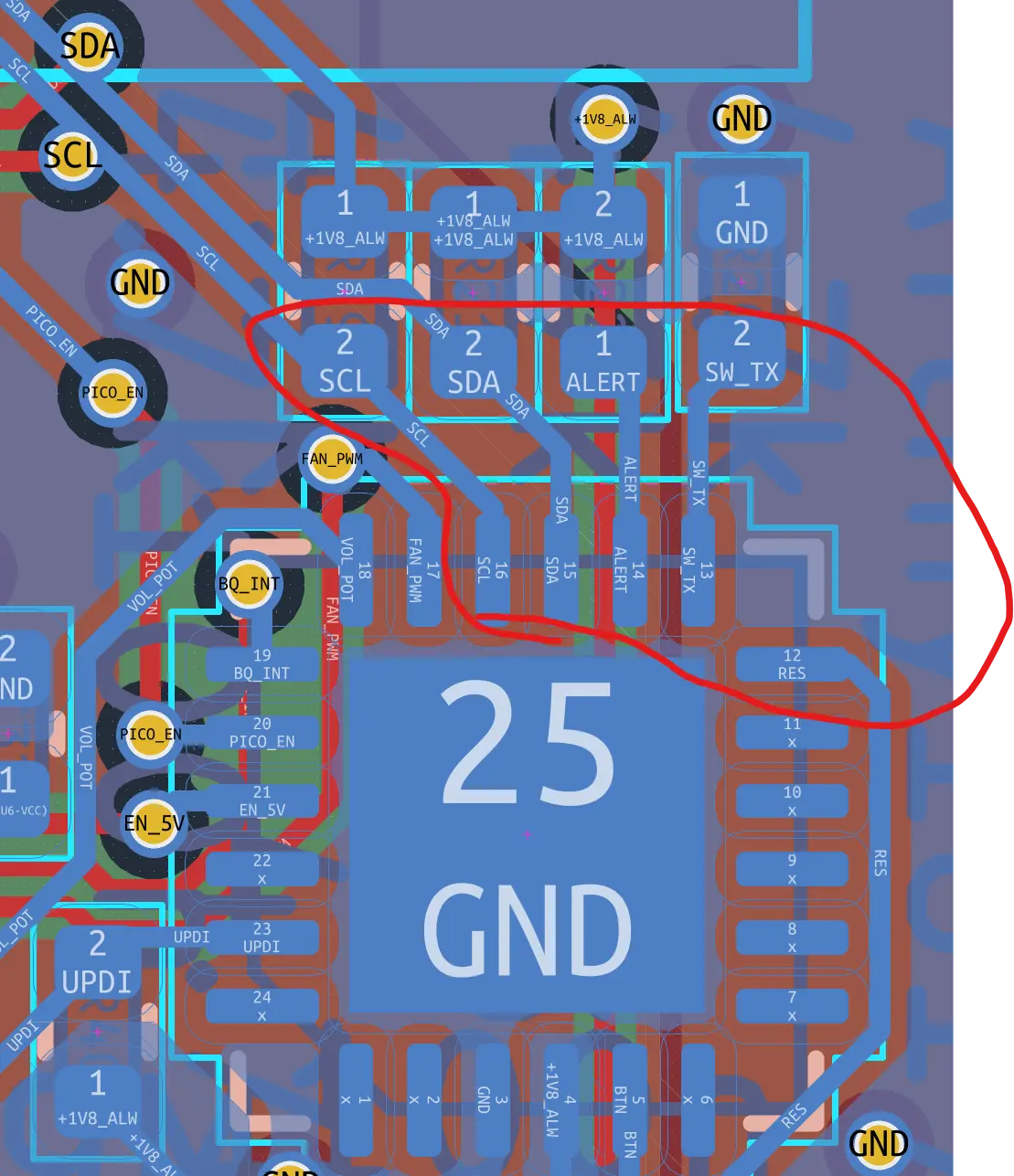
At this point I was feeling really ill, and ended up taking a break… Nothing was working, and I was too sick to think clearly… So a few hours break would not hurt right?
I didn’t do any more work on Saturday… And Sunday was worse… Though it started clearing up towards the end of the day… But I had still lost the weekend… Fuck I’m suddenly a lot lower on time than I expected…
Monday morning, I feel better, but decide to skip Uni. It gives me one day back where I can work sole on this!
I resolder the Tiny, and the Port B pins work again, it was just a bad solder joint on one side of the Tiny. But SDA is still shorted… I manage to trace it down to the riser. Without the riser the short goes away. With the riser installed, there is a shot on SDA to ground. And a short on 3.3V to ground. And Bluetooth Data + and – are shorted together… That is odd. But at the time I assume that the receptacle has an issue where the pins are slightly too big and it might cause the plastic between pins to break and short out. (That was wrong, but it was my assumption at the time XP )
I cut the neighbouring pins for all the shorted ones, I cut the ground next to SDA, and the ground next to 3.3V, and the two BT lines as I’m not using them, and it seems to work. SDA is no longer shorted, and the Tiny is reacting as it should. The GBAWii4 is alive again!
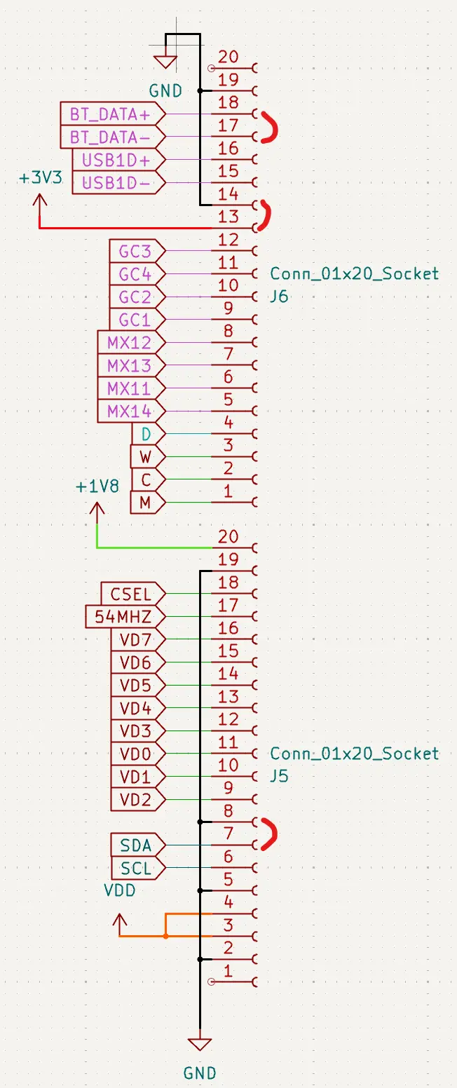
Now does the Pico work with the GBAWii4? Nope XP
I cannot boot while the Pico is inserted… And if I boot first then insert the Pico while the GBAWii4 is running, I end up seeing something weird… The battery rail, supplied by a power supply, drops quite a bit, and the Tiny stops responding properly… And I do sometimes get the 1.8V return voltage, but I don’t get the 3.3V I’m expecting, instead I get 0.6V…
I start by trying to eliminate what the issue is, by putting tape over the pins on the Pico.
Only connecting the power and ground? They are both happy!
Connecting I2C? Nope the Tiny stops responding. I assume they get stuck in a race condition of who is talking on the line… I’m low on time, and the I2C lines between the Pico and GBAWii4 are not critical. Cutting them would stop them from talking, so the GBAWii4 can’t get the temperature from the Pico, so I have to set a fixed fan speed. And the Pico can’t get the battery voltage and usage. But both of these features are optional, so cut it is XP
Oki it works better, but when I remove the tape on the 3.3V line, the voltage drops and the BMS and Tiny browns out…
I was still not 100% healthy, so I decided to leave it there, and started soldering the Zero instead XP Then I spent the rest of the Monday trying to figure out how the WavePhoenix firmware worked… While having a headache still… It was built on an older SDK than what I had, and it was causing issues…
Tuesday, I go to Uni, then come back tired… I think I did some final things on the case and started final prints. And kept poking the issues on the GBAWii4.
The final day
Wednesday, I have only one lecture in the morning, so I had the whole day to get something working, and as the deadline is 5am in my time zone, I got most of the night as well. XP Though I’ll will need to cut down on what plan to do, I need a minimum viable product. A worklog takes hours to write, so yeah that’s gonna be cut… But as long as I get the GBAWii4 working, that’s all that matters. And if I fix the 3.3V issues, it should just work…
Oki so how do I fix the 3.3V issues? When I connect the Pico, the 3.3V is only 0.6V, so there something funky going on. Now 0.6V does that not look like a diode voltage? Could it be that there is a short pin to some kind of voltage protection? I did have that voltage protection of VDD+0.5V on the Tiny, and this kinda smells like that.
Multimeter in diode mode, and sure enough I get 0.6V. So, there is something there! What’s the easiest way to find what components is causing the issue? Desoldering every component one by one! It might take time, but it is a sure fire way to find the issue!
What is on the 3.3V rail? The Audio decoder, MX, SD to USB bridge, FPGA for GCVideo, and the HDMI MUX. The FPGA is the worst one by far, so let’s take that one last.
Audio decoder removed, diode mode still reads 0.6V…
MX removed, 0.6V.
SD to USB bridge… 0.6V
HDMI MUX… Nope…
FPGA… Yeah, the issue went away… but fuck…
Soldered the FPGA back and… 0.6V… What?!
Wait am I being stupid? Let’s connect an external 3.3V voltage to the rail… And I get 3.3V… The 0.6V diode was never the issue! Fuck me!
Solder all the components back… And the external 3.3V still hold.
Okey, lets have a deeper look at this, lets probe the riser. Oh the 3.3V pin is Open Loop… The pin was not soldered properly… the 0.6V was back feeding voltage… Well that was a lot of wated time. But all I need to do is solder that contact right?
Let’s take a closer look at the riser, the 3.3V pin is the 7th pin from the left. 1, 2, 3, 4, 5, 6, 7… Hmmm that is odd, looking at the back of the riser… Pin 7 is ground? What? WAIT! Pin 2 and 3 which is the Bluetooth pins are connected together on the copper! That is the copper meant for VDD, which is pin 2 and 3 from the right! OMG I FLIPPED THE RISER!!!! ALL THE SHORTED PINS WERE BECAUSE THE RISER WAS SOLDERED IN REVERSE!!!!!!! SCL ended up where there was a ground pin, same with 3.3V, what is why I got a short on them, it was not the receptacle breaking, it was the god damn riser!
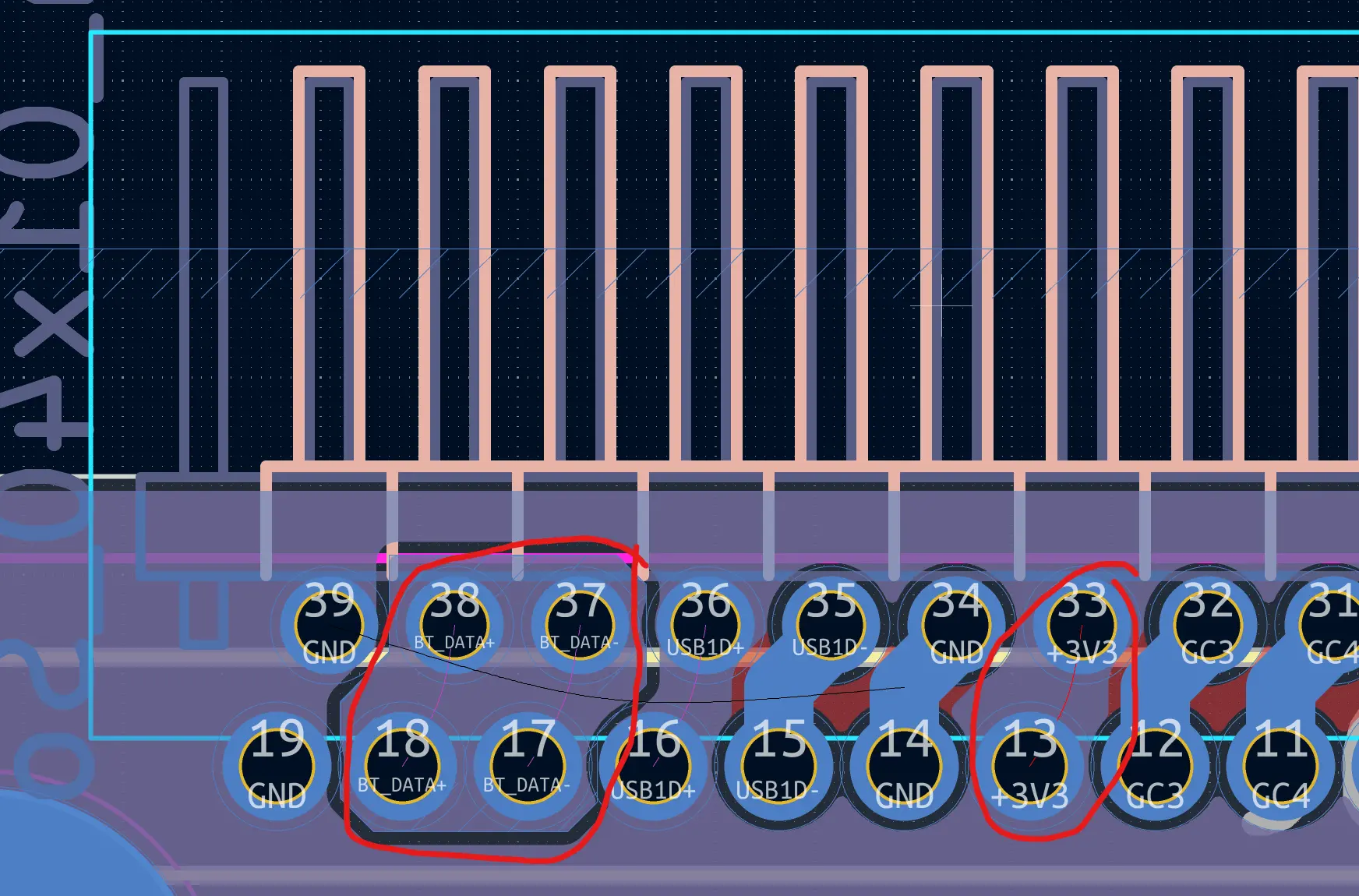
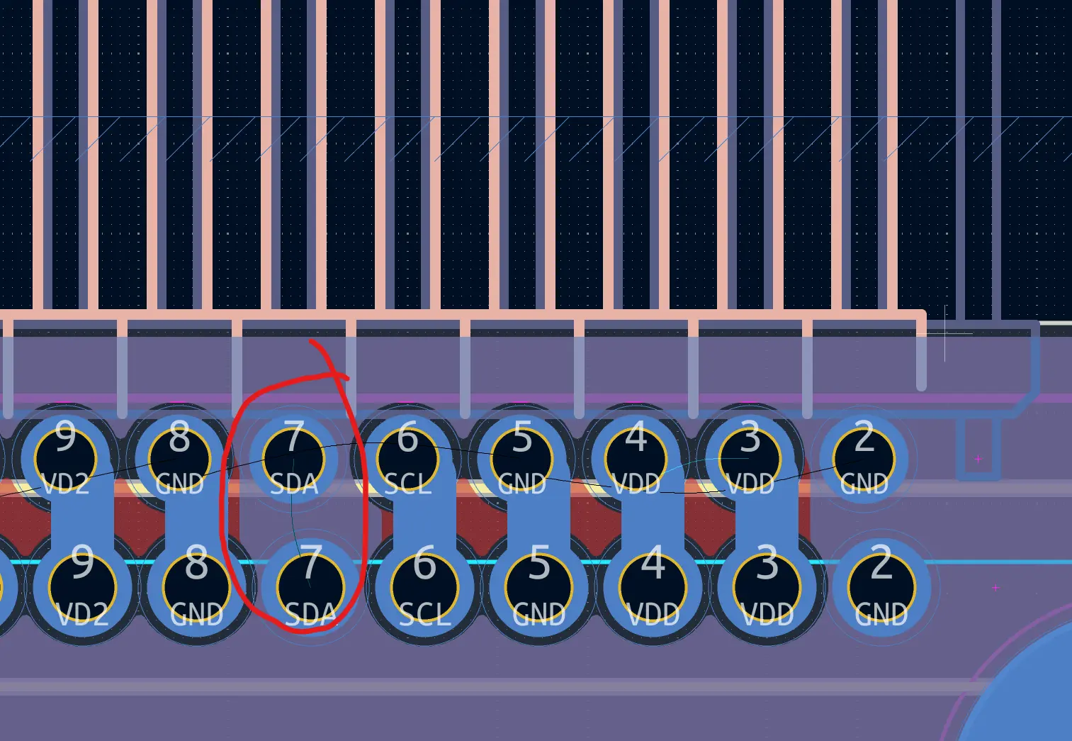
Okey, but that’s fixable, I just need a new riser. I’ll desolder the pogo pins as I don’t have backups, then I’ll solder them on the new riser after making triple sure the orientation is correct. The silk screen is on the wrong side, not sure why, and it does not matter now.
One set of extracted pogo pins later, and it’s time to solder them. Aaaaaaaaand there is solder on the wrong side and it’s bridging pins… Fuck! They are important pins! Double fuck!
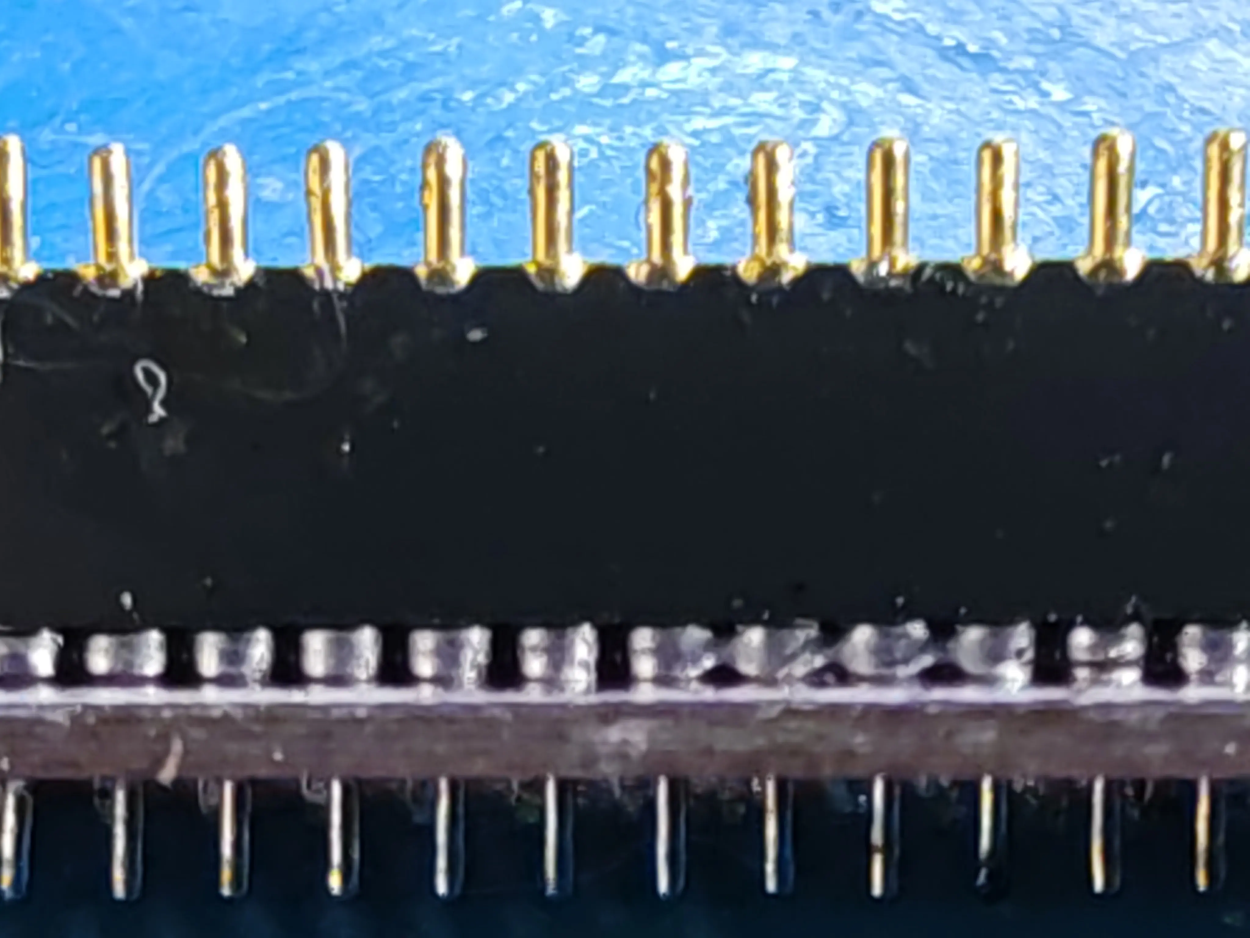
Okey maybe if I use some solder braid I can wick it clean? First attempt… Nope, I just melted the plastic of the Pogo pins… Well I can just try again… Fuck I’m low on solder braid, I only have about 4 uses left… Let me check I think I have some more somewhere… Nope can’t find it… Maybe B&Q sells some? Yes they do! Wait this is the UK website, let me switch to Ireland to check if my local one has some… Nope B&Q Ireland does not sell solder braid/wick… Fuck… I have no clue if there is any other stores nearby which sells any, and I don’t have time to travel around and check…
Oki I got to make do with that I have… The soldering iron does not reach deep enough, so what if I just… Cut… The plastic? It’s not the cleanest solution, but it is a solution!
Some plastic shavings later, and it seems like the iron will fit in! Oki let’s take one of the remaining solder braid pieces I have and give it a shot! Aaaaaaaaaand it worked!!!! I managed to clear the solder bridge!!!! Whoop!
Alright, let’s plug the riser in, and see if it lines up with the Pico still…. Nope… It’s angled slightly too low, and won’t hit the targets… Damn… Lot’s of finicking later, and I found that if I pull the riser slightly out of the receptacle, it will line up. Maybe I can make a spacer? But that is a later me problem, for now let’s test!
The voltage drop is still there… And now the GBAWii4 freezes after plugging in the Pico… And checking voltages, it does turn on! I do get 3.3V now!!! But 1.8V only shows up sometimes… It seems the riser not being seated fully leads to a bad connection… But let’s at least check if it is running… The 54MHz video clock… Is 54MHz!!! The Pico is still booting and running!
Okey at this point fuck the riser, I’m tired of messing with it. I need the shell to support the Pico to make it aline with the riser, but that blocks me from poking most of the board, so I can’t find that voltage drop… It’s getting late and I’m out of time… Magnet wires worked before, so I guess I’ll just hard solder it… It won’t be pretty, but as long as I get it working, that is all that matters.
Time to disassemble the Pico, remove the pogo targets… Using two of my remaining solder braid lengths… And needing to fiddle with the holes to clear the last few…
Hmm, the pin pitch for the connector is 1.27mm, I’m sure I have some ribbon cable which is supposed to be 1.27mm pitch. That would likely look nicer than just going magnet wire. Oh, I found it!
Time to strip, twist, and tin 38 ribbon connectors. Then stick them into the Pico one by one and solder them… Ehm… That ended up taking a lot more time than I had planned… But oh well, it looks kinda cool, it’s like an IDE powered Wii now XP
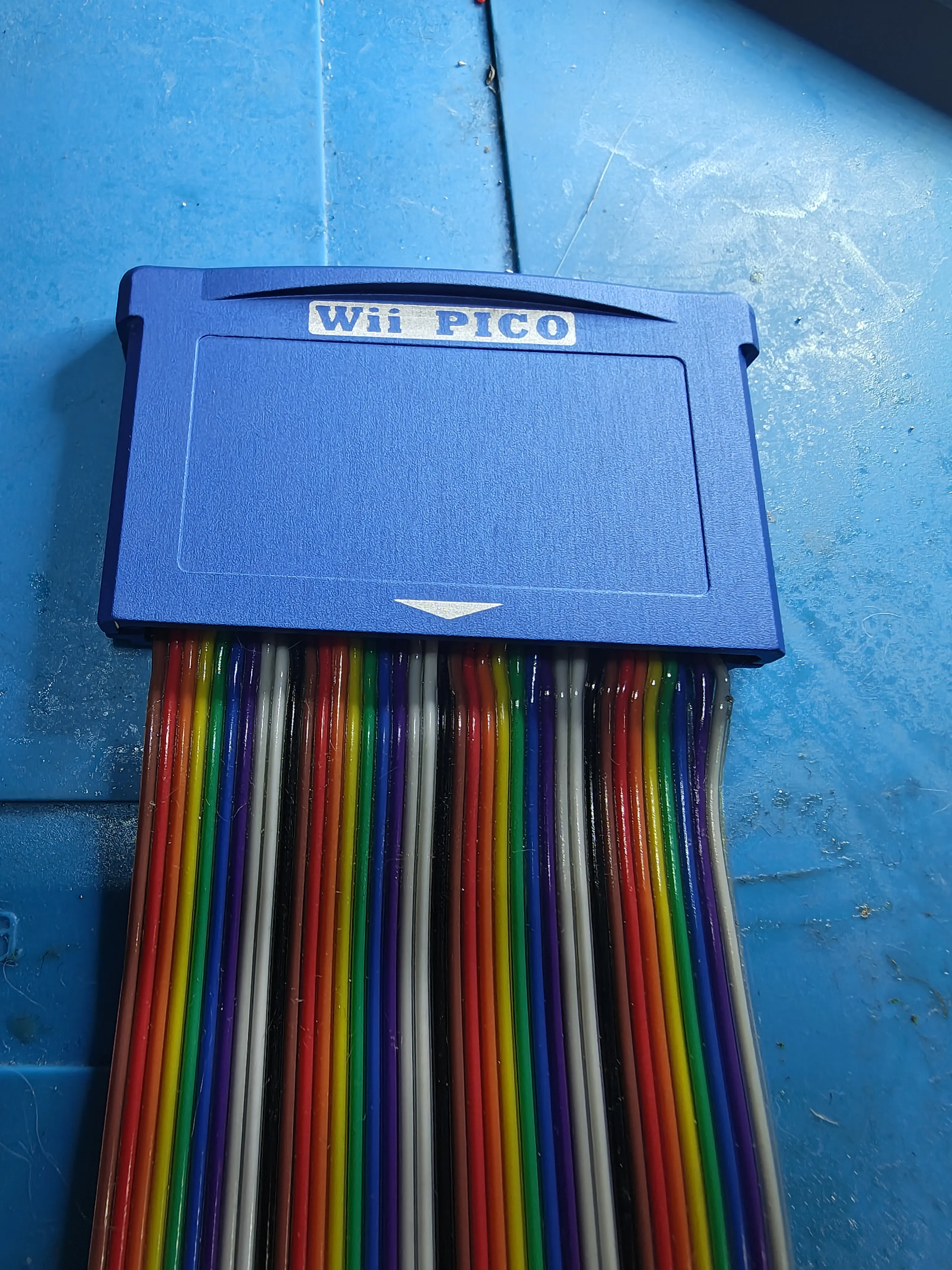
Now let’s strip twist and tin 38 more connectors for the other side… At least I have some practice XP And I’m going to only solder a few of the connectors first, I want to know why the voltage drops, and if there is some specific pins which causes it.
I desoldered the pin header from the first riser, and soldered VDD and Ground.
Then connected the Pico… Please boot… Please boot… It boots! But there is still a voltage drop… Where the fuck does it loose 1V? There must be a high resistance somewhere… Is it the power switch to the pico? No… Is it the BMS? No… Hmm the voltage going to the battery pad is also low… What about the connector between the PSU and the GBAWii4? There the voltage is correct! Wait is it the wires between the connector and GBAWii4? Yes! Touching them and they are hot! I’m using to low of a gauge wire for the current going through it!
Okey, quick solution, what is the thickest wires I have? 16AWG? Yeah that should do it! Aaaaaand the voltage drop is gone! The brownout of the BMS and Tiny no longer happens! Problem solved! Maybe I can make it in time!
Let’s solder all the remaining wires to the Pico and test it! It turns on! Let’s check voltages. 1.8V? Check! 3.3V? No… What? Let’s check on the Pico side. Yes the 3.3V is there. Let’s check on the end of the ribbon cable… Yes 3.3V. On the underside of the GBAWii4 where the receptical is soldered? Nope… What? Okey let’s unplug the pins and check. It’s pin 7. 1, 2, 3, …, Wait pin 7 has been cut?!
Do you remember how I had some shorts on the riser early on, and I thought it was due to pins touching in the receptacle? And how I cut the adjacent ground pin that I though it was shorting to? Well turns out I can’t count, I cut 3.3V and SDA, not the ground pins next to them… XP
Okey it’s all coming together, it explains more of the issues I had, but for now, lets cut the pin header up, and solder the 3.3V pin onto a new pin.
I plug it in, aaaaaand it stops working… Fuck… and at this point it’s late into the night… I’m out of time…
If I unplug the 3.3V pin, it boots, and if I plug it in while it is going, it works. If I turn it off and on it work. But if I leave it off for a while and then turn it off, then it does not boot… Is there some kind of startup rush which kills the system?
Dumb solutions, I’ll take the Pico apart again, program the Tiny on it to have lots of long delays. How about a 1 second delay from the Tiny gets power, till it turns on the regulators? Then a 1 second delay from the regulators turn on till it releases reset on the Wii? That should have plenty of time, right?
I solder the programmer on, and try to program it… It does not work… Wait why is the programmer power light off? Why is the programmer really hot??? I unplug it and check my wires… I had gnd and vdd reversed… Fuck! Oki wires fixed. Let’s plug the programmer in… Why is the power light flickering?... Check resistance… VDD for the tiny and ground is short… Fuck…
Time to desolder… It’s the Tiny… Resoldering it and the short goes away! But the programmer can’t talk to it… Fuck did I kill the Tiny? I don’t have a backup…
Let’s check my old projects again, maybe I have a ATTiny1617 or 3217 somewhere? Oh found one! It’s from a project I will use in a few weeks, but that is a future me problem. Before I desolder it, let me check that I can program it… Nope, the programmer does not want to talk to it… Did I fry the programmer as well?
The only other programmer I have that can work is my Snap, but I would need to use MPLab, and I need to supply external power… Some finicking around later and I validated that the Snap could program the Tiny on the other project. And that it can’t program the Tiny on the Pico… Oh well… I need a new UDPI programmer, and a stockpile of Tiny1617, as I’ve killed 2 so far.
Some desoldering and resoldering later, and the borrowed tiny is on the Pico, and it has been flashed with the updated firmware. Let’s see if it works. It starts booting! Then after 2 seconds the power light turns off… Fuck! What! Why! It’s so late in the night, I only got ~2h left of the deadline, and I’m tired…
Hmm the 3.3V rail is active, and 1.8V… And the video clock. Wait it’s running! But it does not react to the power switch… Let’s check some things… Oh the SCL is stuck at 1.2V! Oh, the firmware gets stuck as it’s waiting for the I2C to be clear! Disconnecting 3.3V and it works, nothing is holding up the I2C lines. Connecting 3.3V and I2C stops working… What is connected to I2C which is driven by 3.3V? The audio decoder. Well that is not critical! Desoldered! Oh, it works now! The power switch can turn it on and off, the pico is giving out voltages, and the video clock is where it should be! Maybe I can still do this? I just need an image!
The fastest way to check if I have video is MelonHD, I just need to plug in the USB C display I have. Plugged in. WAIT!!! Unplug. I’m still using a power supply instead of batteries. I’m not sure how happy the power supply will be when the BMS is trying to charge it XP. Okey time to solder the actual batteries in! One battery needs it’s wire extended. Then it’s stripping, twisting and tinning them. Then soldering them. And the console is battery powered!
Okey let’s try again! USB C plugged in. The monitor registers something! It sees it as an option for KVM… It does not see it as a video input… Maybe a USB C to HDMI dongle will work? If I can find it?... I did not find it…
Oki MelonHD is out, I’m to tired to try and figure out why. But maybe the internal display works? I just need to solder the wires. I already soldered all the wires on the driver board, so I only need to do the final half… Damn these wires are small… And why are my hands shaking? God I’m tired… Okey that is one soldered… And two… And one of the wires on the driver board pulled loose… Yeah no… This will take too much time… There’s about an hour left of the competition… I don’t think there’s much more I can do… Fuck…
Okey back up. I have the Zero, I just need to solder the Pico Rev 1 to it, and it should just work. Then I can show that the Pico and Zero works. That was supposed to be the backup anyway, but the plan had been to solder and test the Zero during the weekend, but since the components didn’t arrive, it ended up being delayed. But maybe I can pull it off in this last hour?
Oki it’s all soldered up, let’s test it… Does it work?... No… Let’s poke around… I get voltage in, but the 3.3V regulator is not turning on… Fuck… I don’t have time to figure out why…
There is 30min left before the deadline… Oki let me put the GBAWii4 together as much as I can, and let’s make some videos at 04:30… Swapping over to final cases, and inserting all the buttons, lining the rubber domes up, screwing everything together… It’s 04:45 by the time I’m ready…
My flatmate sleeps in the room right next to mine, I don’t want to film and speak while he’s sleeping, so down to the living room, and using his desk as it’s a nice clear space. I don’t have time for retakes, so it’s now or never.
I film one video, then decide that I want a dissasabled version as well. So I go upstairs and get my tools to dissasable the GBAWii4, and film the second video… I go back upstairs, it’s 04:58, I can’t wait for the videos to upload to google photos and to download them again. Let’s grab a USB cable and transfer them over to my laptop. I message in the discord that the videos are done and that I’m uploading. Then grab the youtube links while the videos are still uploading, and put them in my worklog. 05:01… One minute past the deadline. But surely that is fine. I did it! I uploaded! Though I feel defeated as I could not get the GBAWii4 or the Zero to work…
There’s only 1 hour till my alarm is supposed to wake me, so there’s no point going to sleep, so I just sit there… I’ve spent months on this… Every free moment… Pushing through exhaustion… And sickness… I’ve delayed university assignments for this… I’ve spent almost two grand on this… And this is the culmination of everything I’ve done and worked so hard for…
There’s a notification in the discord, the voting poll is live. And I’m not on it… What? Fuck! What? Why? Is it cause I didn’t finish? No I’ve been on the poll before with unfinished projects, and there is a 20% bonus for completing you main objectives. Is it cause I was 1 minute late? Surely not… Let’s read the rules again… Oh I need to set the worklog as complete? I completely forgot about while sleep deprived… I switch the tag and ask in the discord what’s up… And yeah, apparently, it was not switching the tag to complete that did it… Fuck… I want to cry… That sucks so much… Everything was for nothing?... I should just have slept… Why did I do this?... God damn I’m stupid…
Some more chatter in the discord… And the moderators allowed me onto the poll as I had been right on the deadline! Whoop! That’s amazing! It wasn’t all for nothing!!! And I’ve learned a lesson in not uploading at the very last minute and making sure I triple check the rules after submitting XP
But seriously, thank you moderators for allowing me on the polls even though I delivered literally last minute.
After that I drove to university after having been awake for 24h, did my first class as it was a group project. Then left as I could not do math while that tired XP (PSA: don’t drive while sleep deprived! XP )
Getting home, I still had to stay awake till the night came around again…
But as I sat there, trying to not sleep, I kept thinking about this whole absurd project… This is 3/3 times that I’ve failed to deliver a working portable in the end. In 2021, I killed the BMS on the last night… In 2025 I ordered the PCBs too late, then they got delayed, and I got sick. I also had several issues that I would have caught had I ordered earlier and actually tested it. And now 2026, a riser being soldered in reverse, drove me to waste too much time before I figured it out. Along with getting sick again. Either I need to order things even earlier so that I can aim to complete my project way before they are due, or I need to accept that I suck at making handheld consoles XP I have plenty of other projects which turned out great and worked as intended, but making a portable seems to be the bane of me XP
Though I did have some stuff working. The Pico and test dock worked, I ordered that way earlier, tested it, and even got a second iteration through. Wait… Isn’t the Pico the more impressive accomplishment? And the Pico actually worked! Both rev 1 and rev 2! I reverse engineered the Wii GPU, CPU and what traces were needed. Made a spreadsheet of all the pins. And figured out how to put the RAM on the backside by moving the DQ groups around! It’s the smallest Wii motherboard ever made! And it fucking worked!!! The GBAWii4 and the Zero were only supposed to be docks which showed off the main accomplishment of the Pico. But as I got the Pico working months ago, I kinda forgot about it as I kept getting tunnel visioned on the GBAWii4 and Zero.
I managed to squeeze a custom Wii motherboard enough that it could fit inside a GBA Cartridge! And that’s kinda amazing XP So what if the docks didn’t finish in time, I made the fucking smallest Wii motherboard in the world!
And I’ll release the project files after I’ve cleaned them up. As I really want to see what the rest of you manage to do with the design! Will we see a Wii Femto? Will we see a Wii inside a Wiimote? Inside a phone? What kind of crazy things can you guys come up with when the smallest working Wii motherboard is just 31x49mm and that includes a ThunderVolt implementation! XP
Though that also leads into a few points. None of that would have been possible without this amazing community, and being able to use the knowledge built so far. YveltalGriffin for the ThunderVolt, Scampi, FujiFlex and MelonHD, all projects I borrowed form to make the Pico and GBAWii4. Loopj for the firmware for the ThunderVolt that I extended for the Pico, and for the WavePhoenix for the Zero. Auralio for GCPlus. B_Rob1 for the first (on the forum) Wii motherboard recreation, his project let me catch some pins I had gotten wrong and let me better label some of the pins on the GPU and CPU. And helped with tips on how to solder GPU and CPU. And a massive thanks to the whole community ^^
Anyway, that’s probably enough for this final update, so this is me signing off, and looking forward to seeing how the competition results turn out tomorrow ^^
Glory shots
Pico Pak
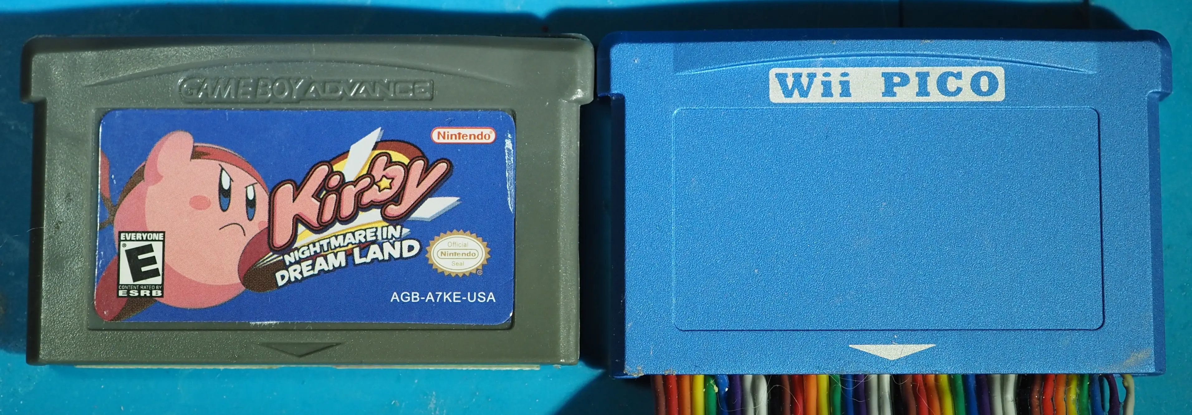
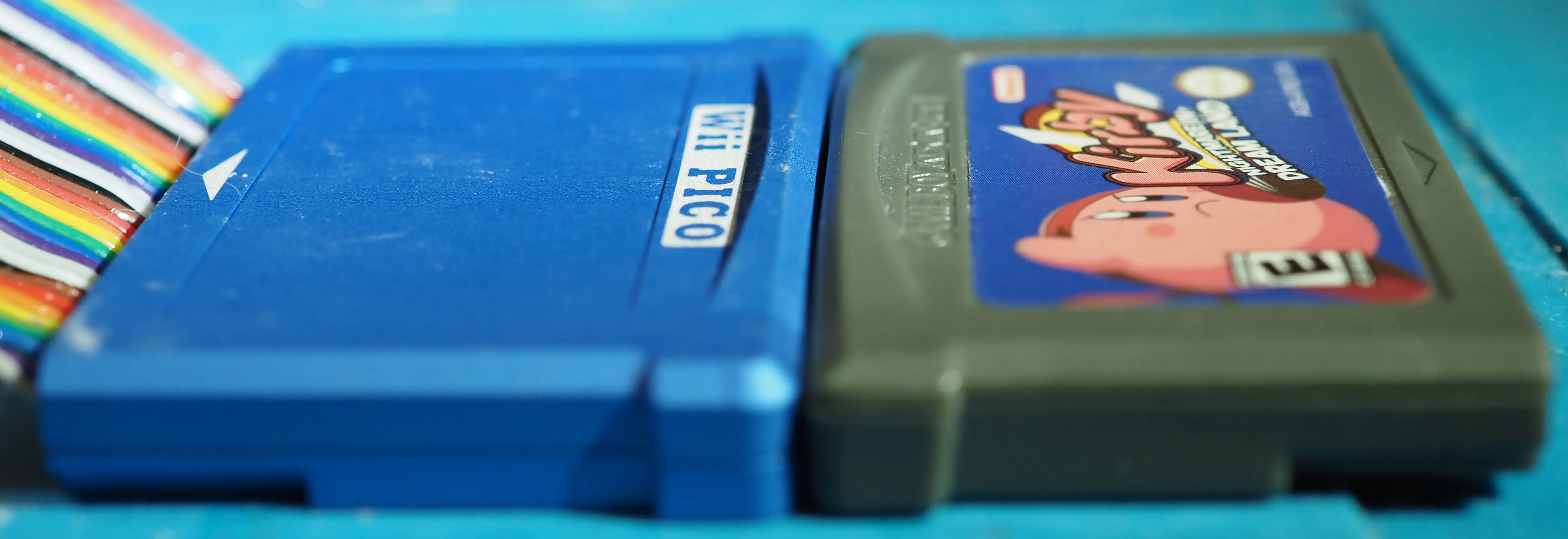
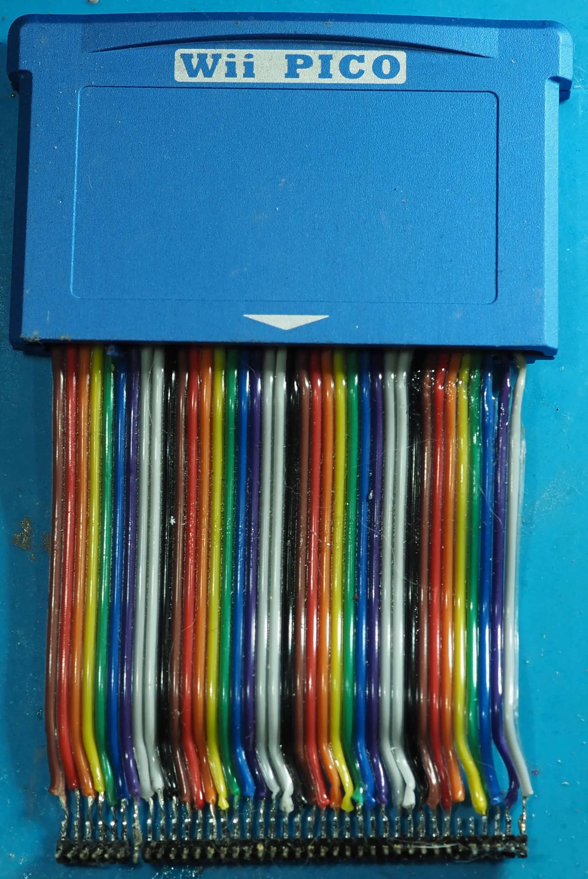
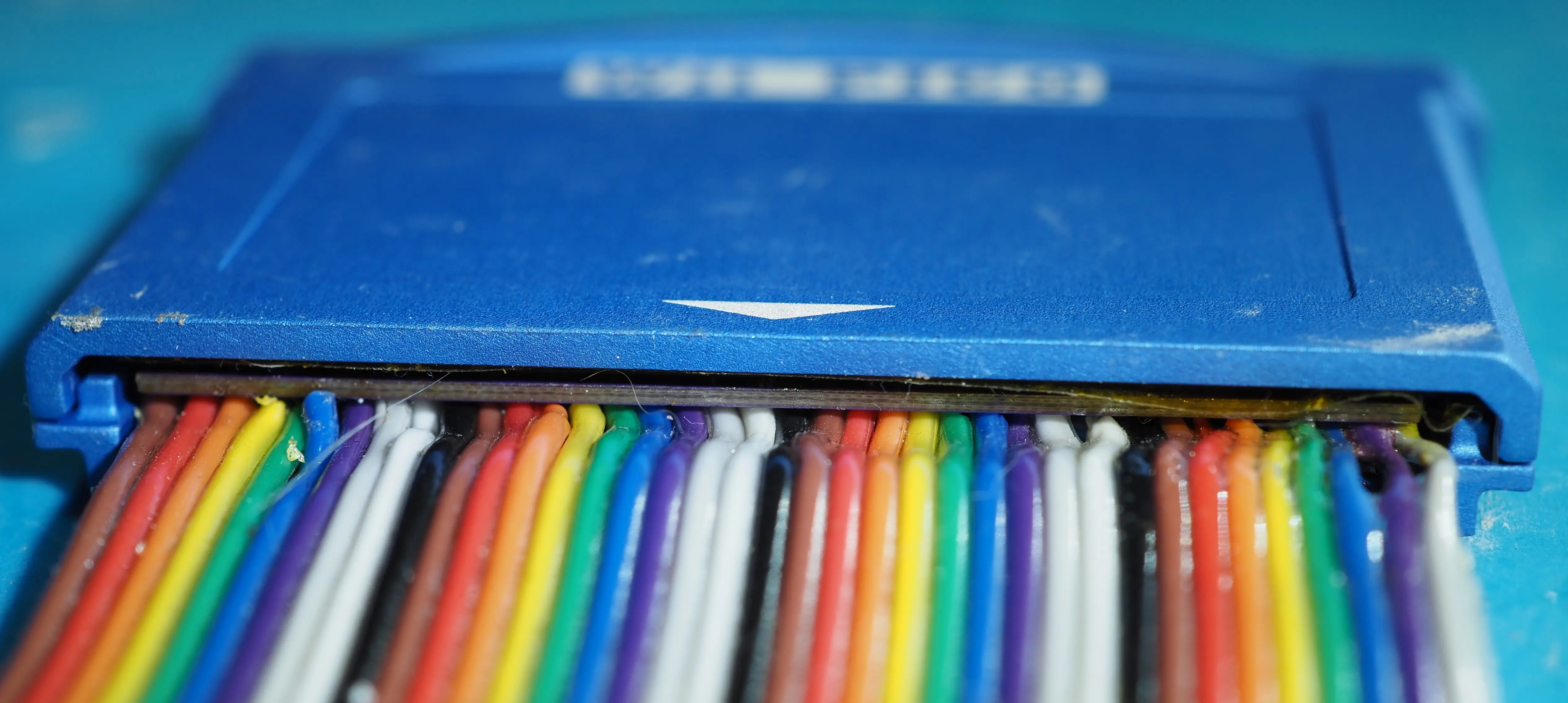
Pico Internals
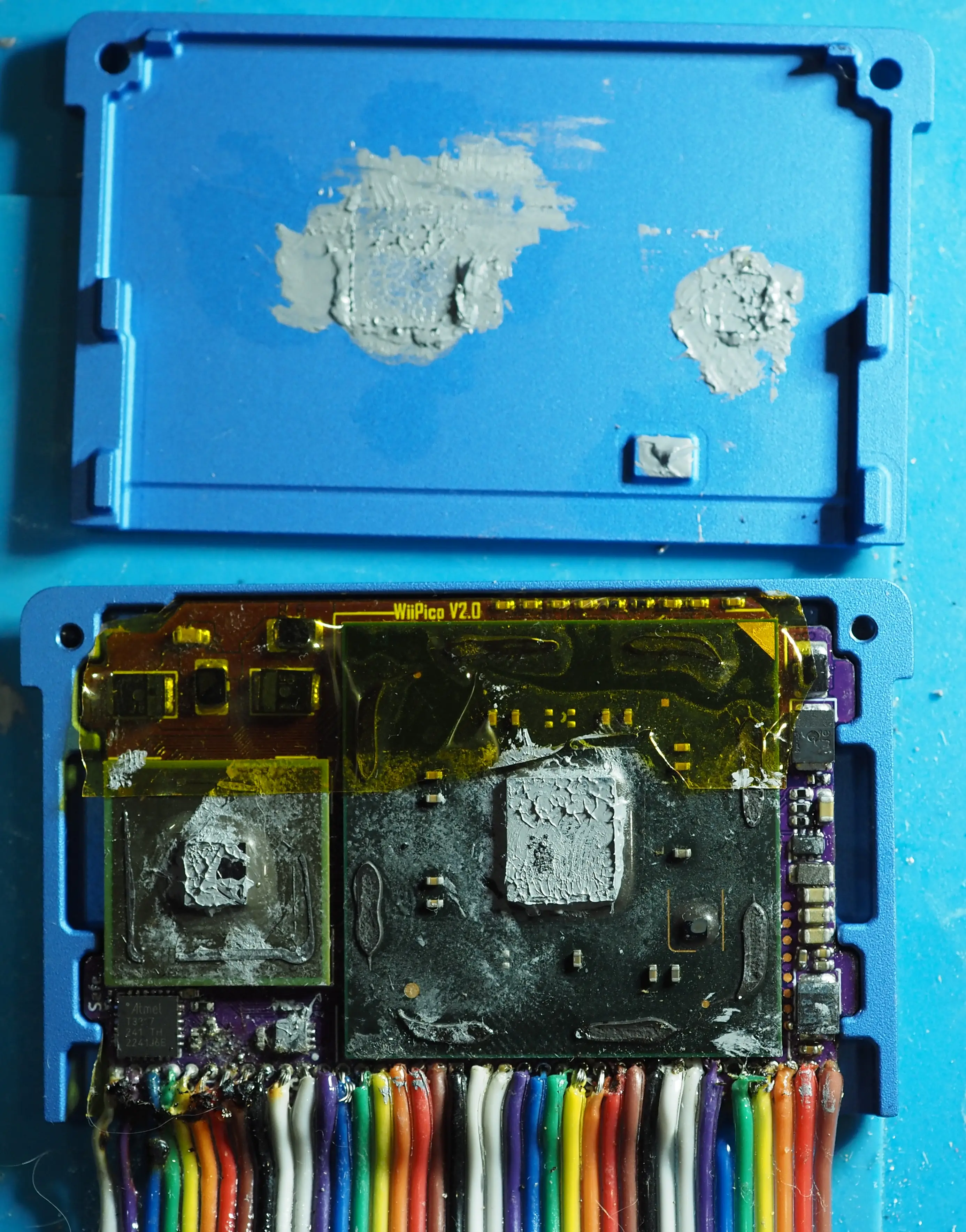
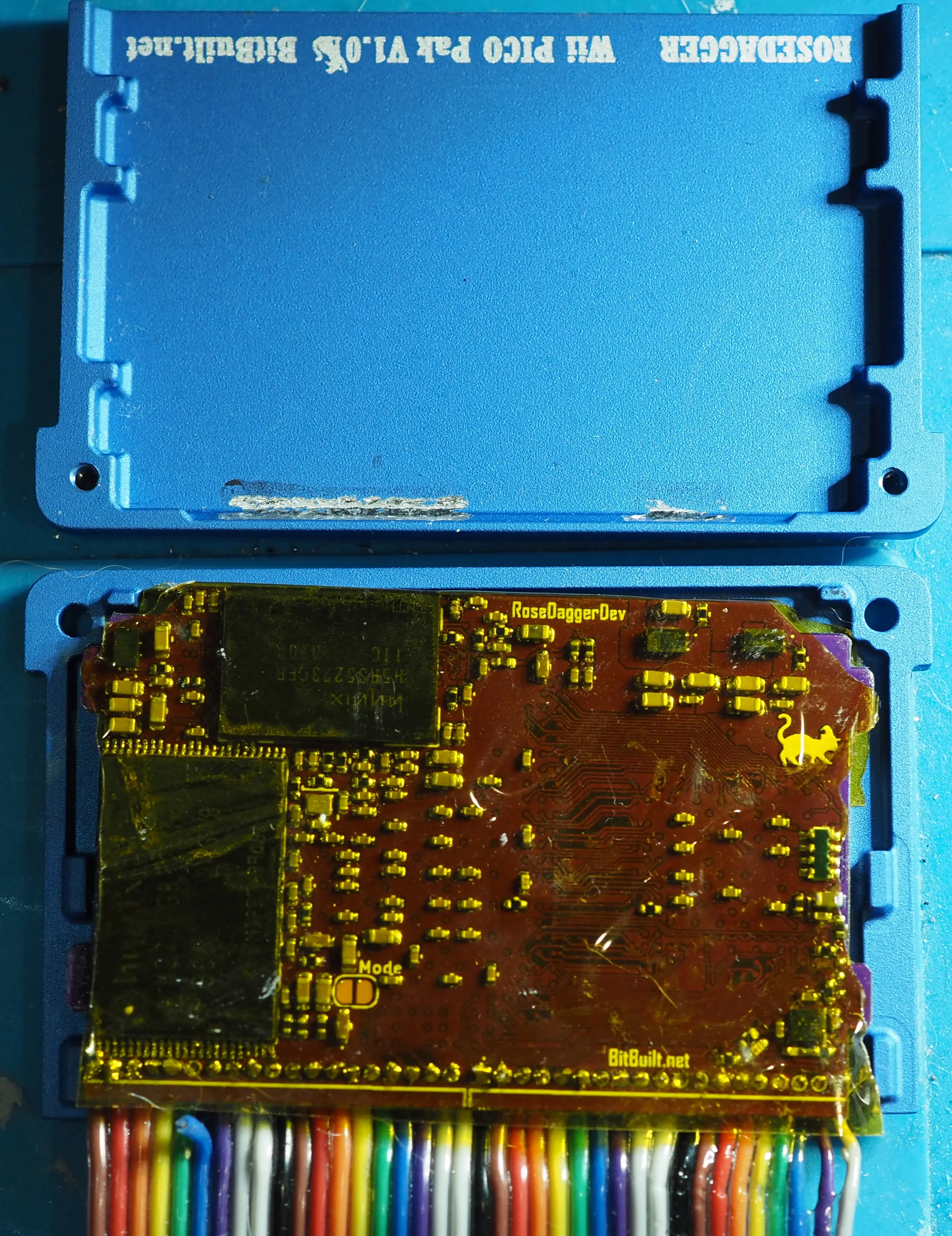
GBAWii4 Shell
The GBAWii4 is not inside so the buttons and joysticks have no supports.
And the glass is scratched as I was checking that I could remove the paint. The screen is slightly larger than the glass frame, so I would have needed to scratch off some of it to make the whole screen visible.
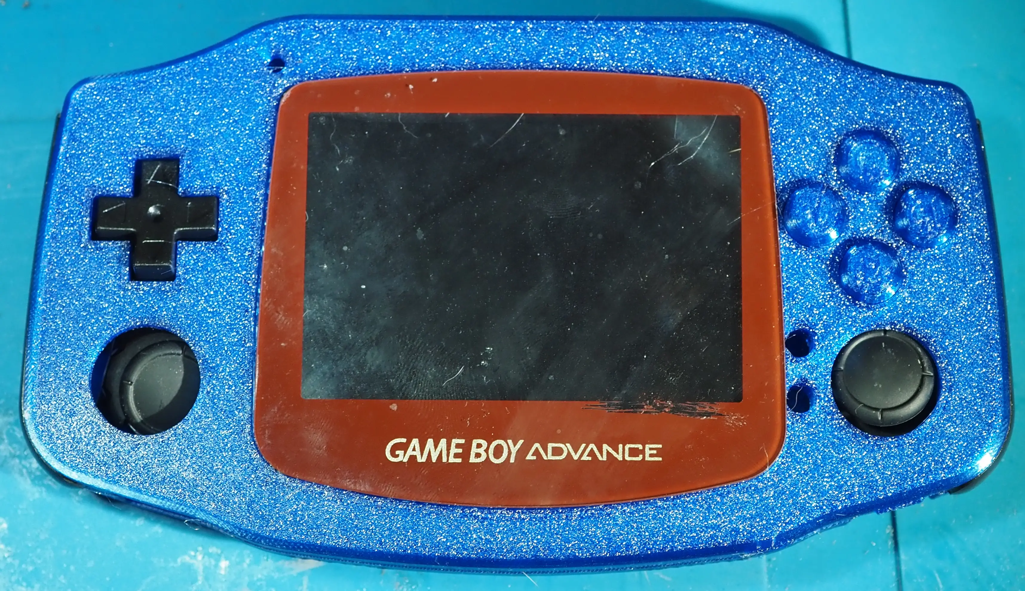
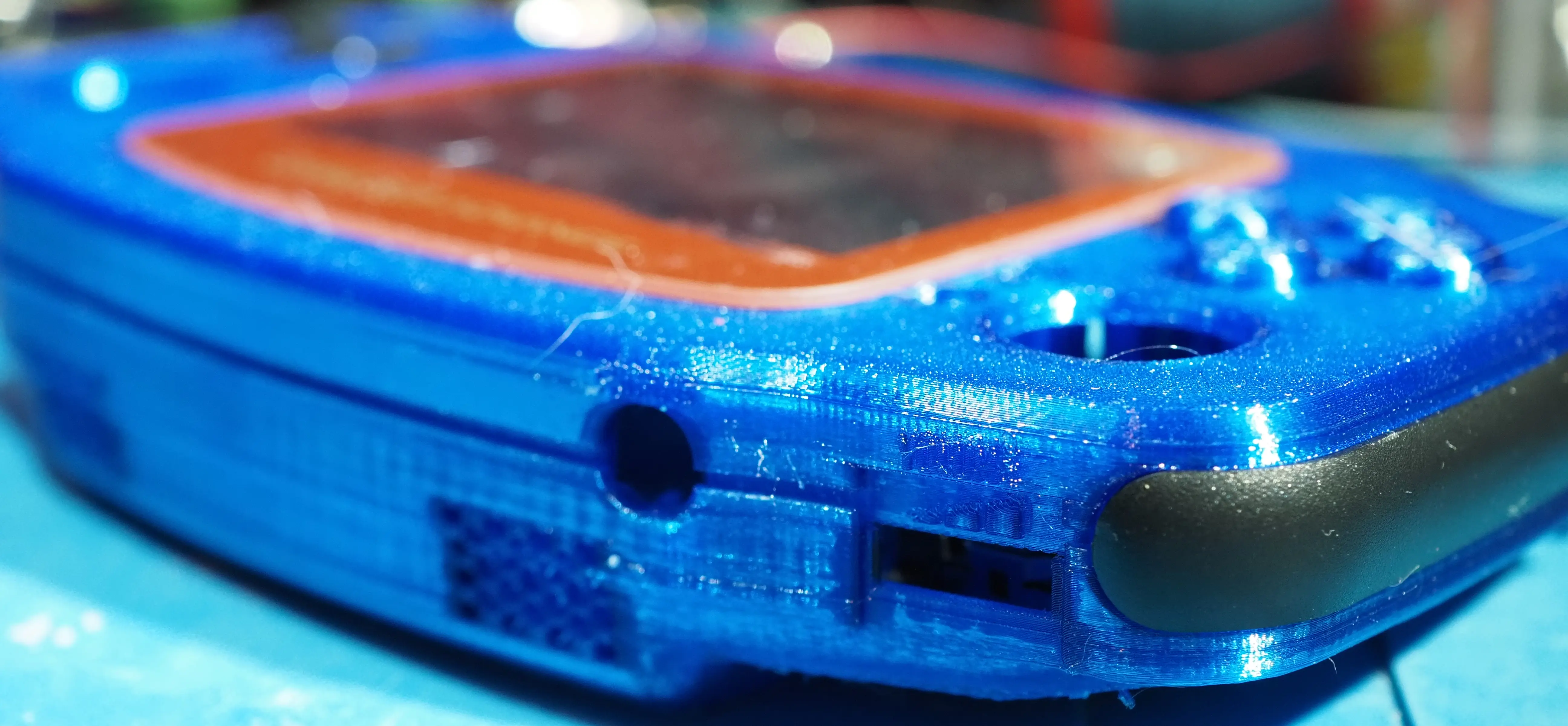
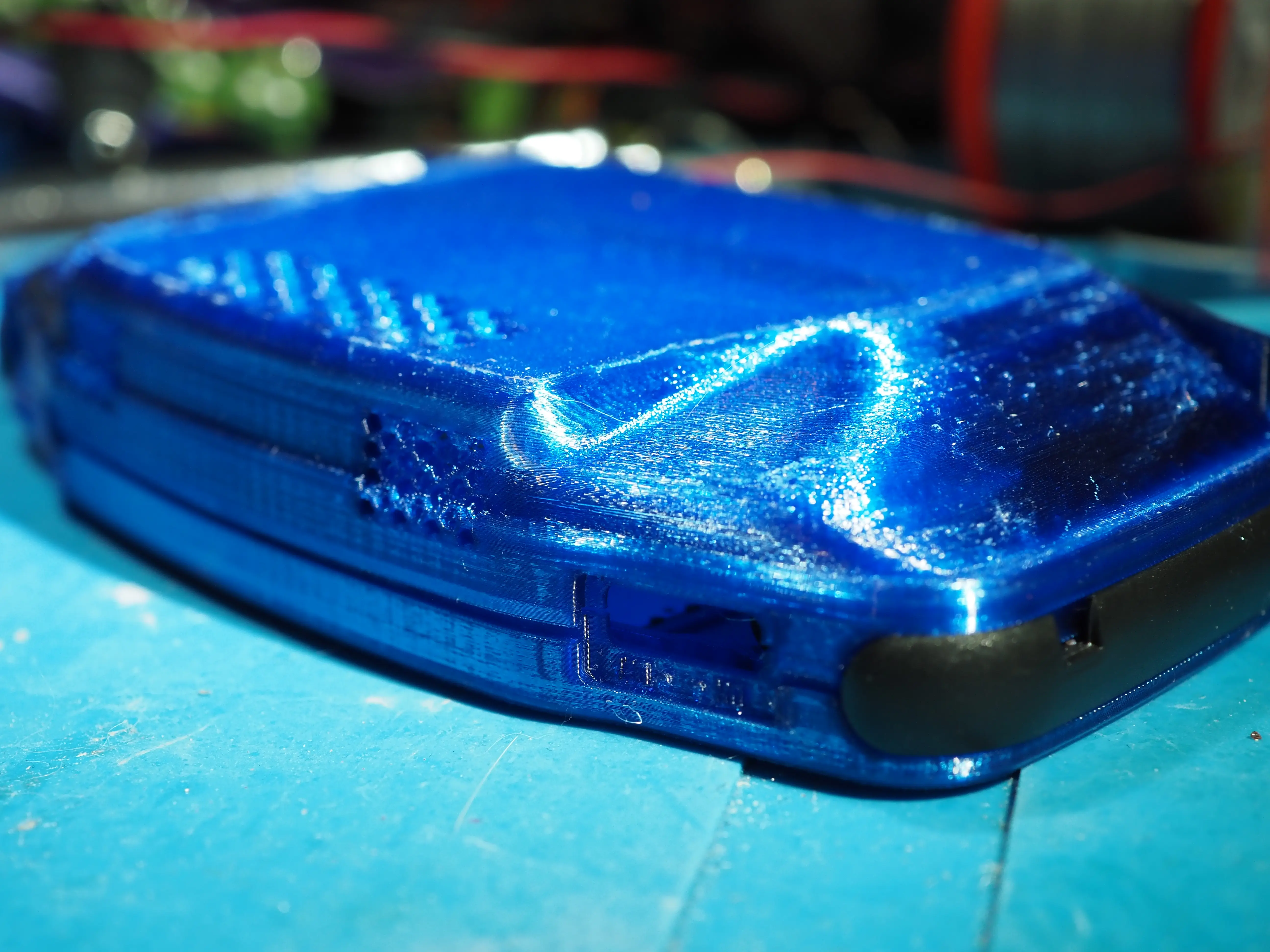
GBAWii4 Internals
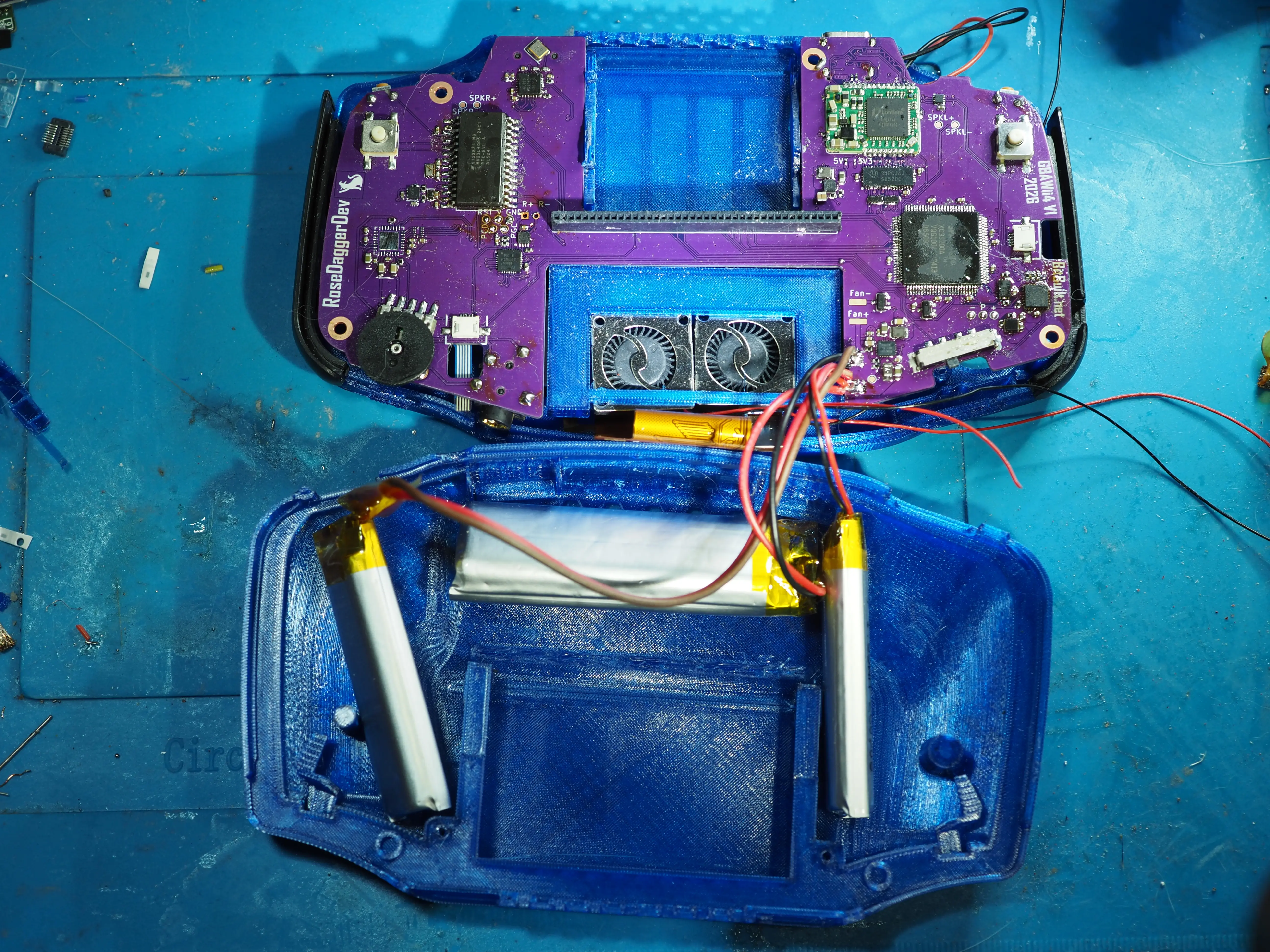
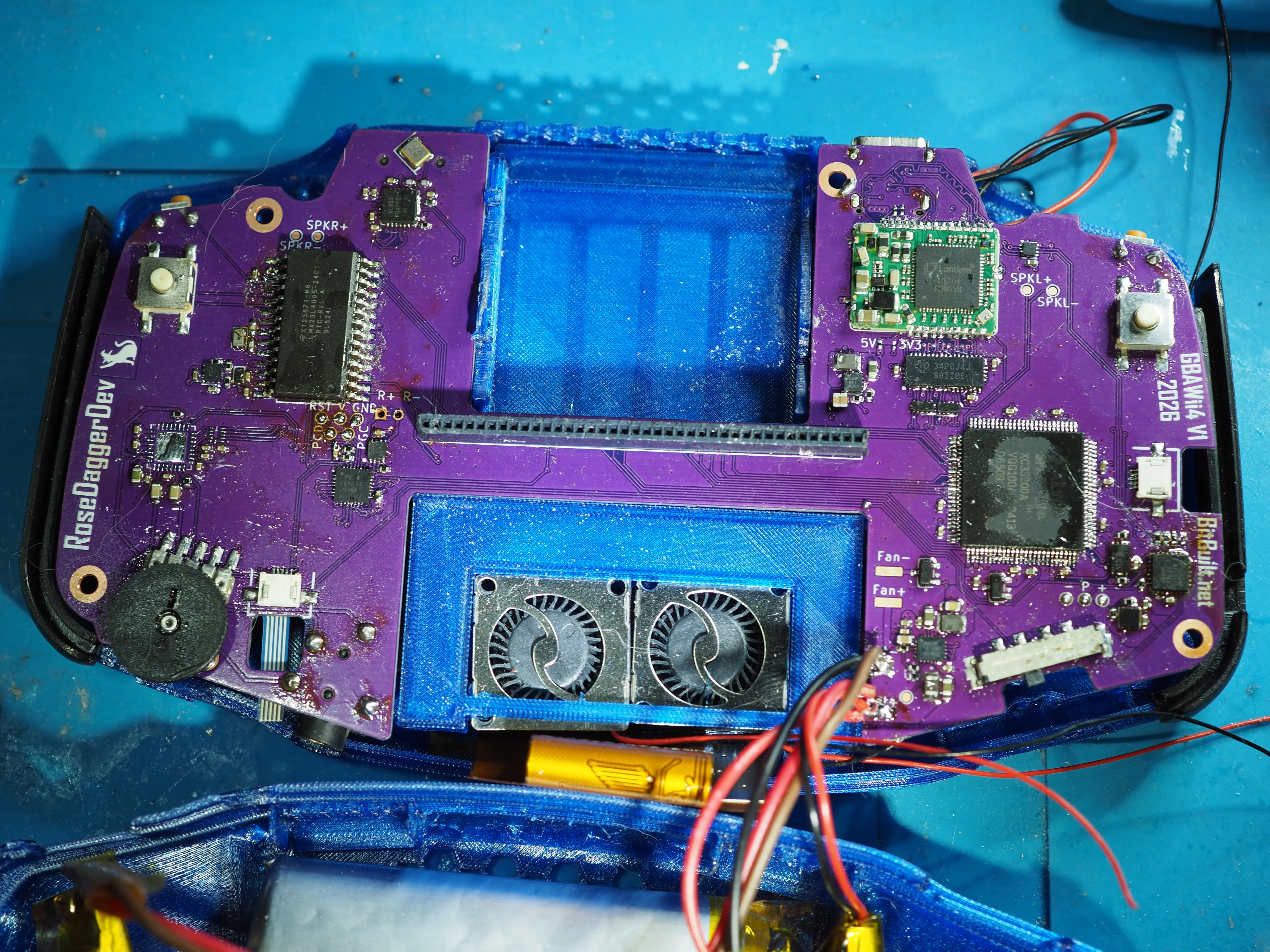
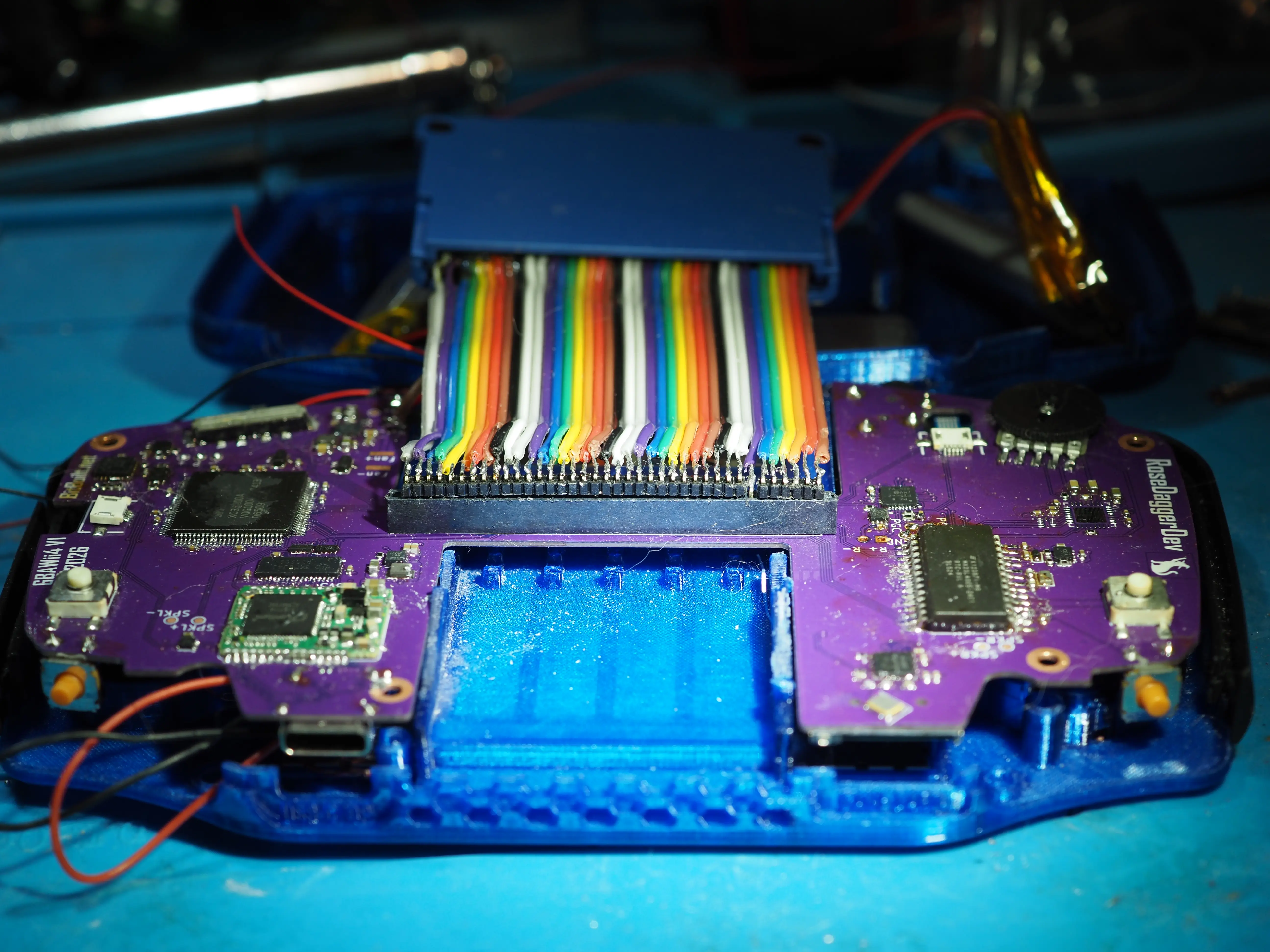
Wii Zero
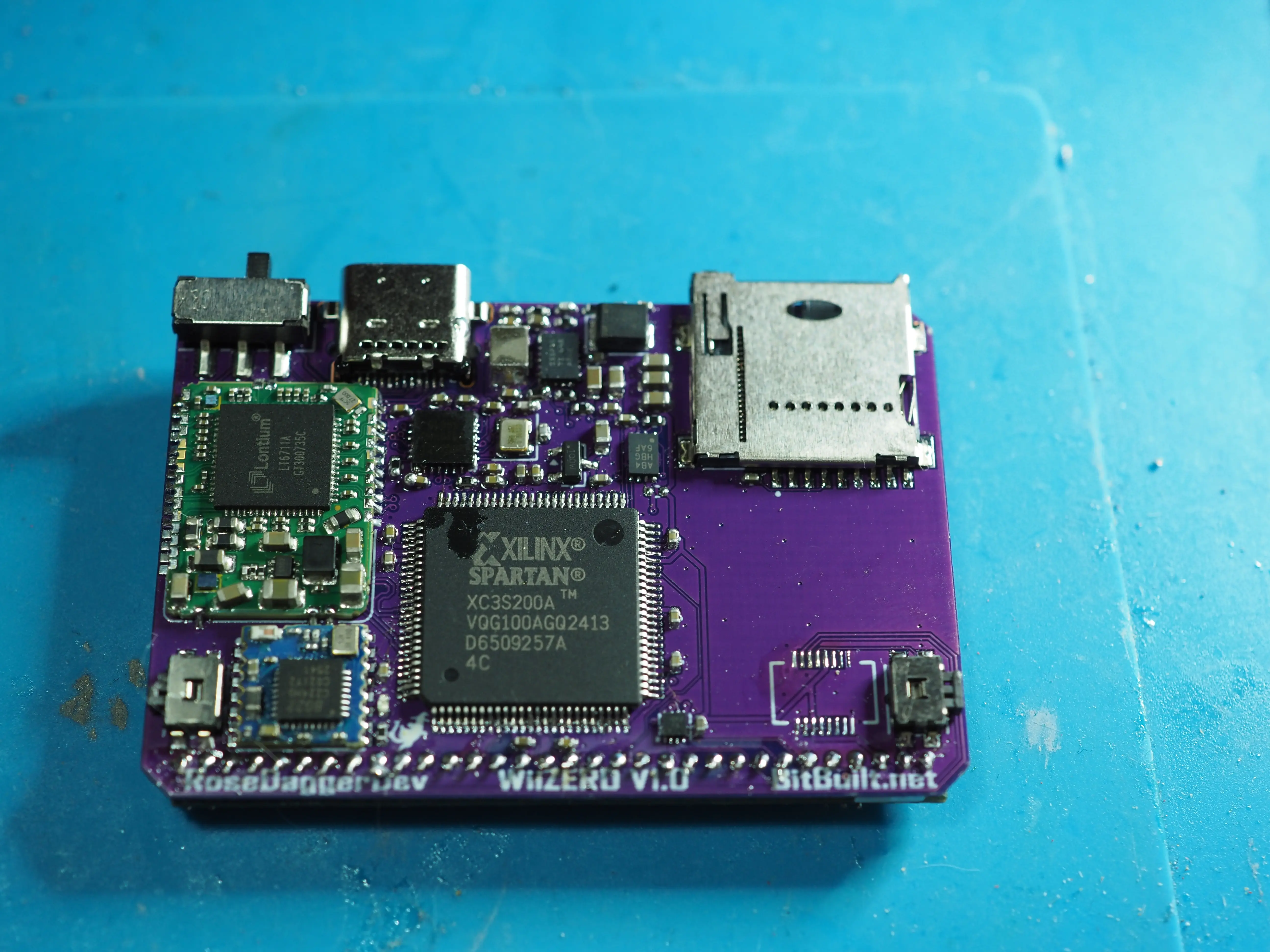
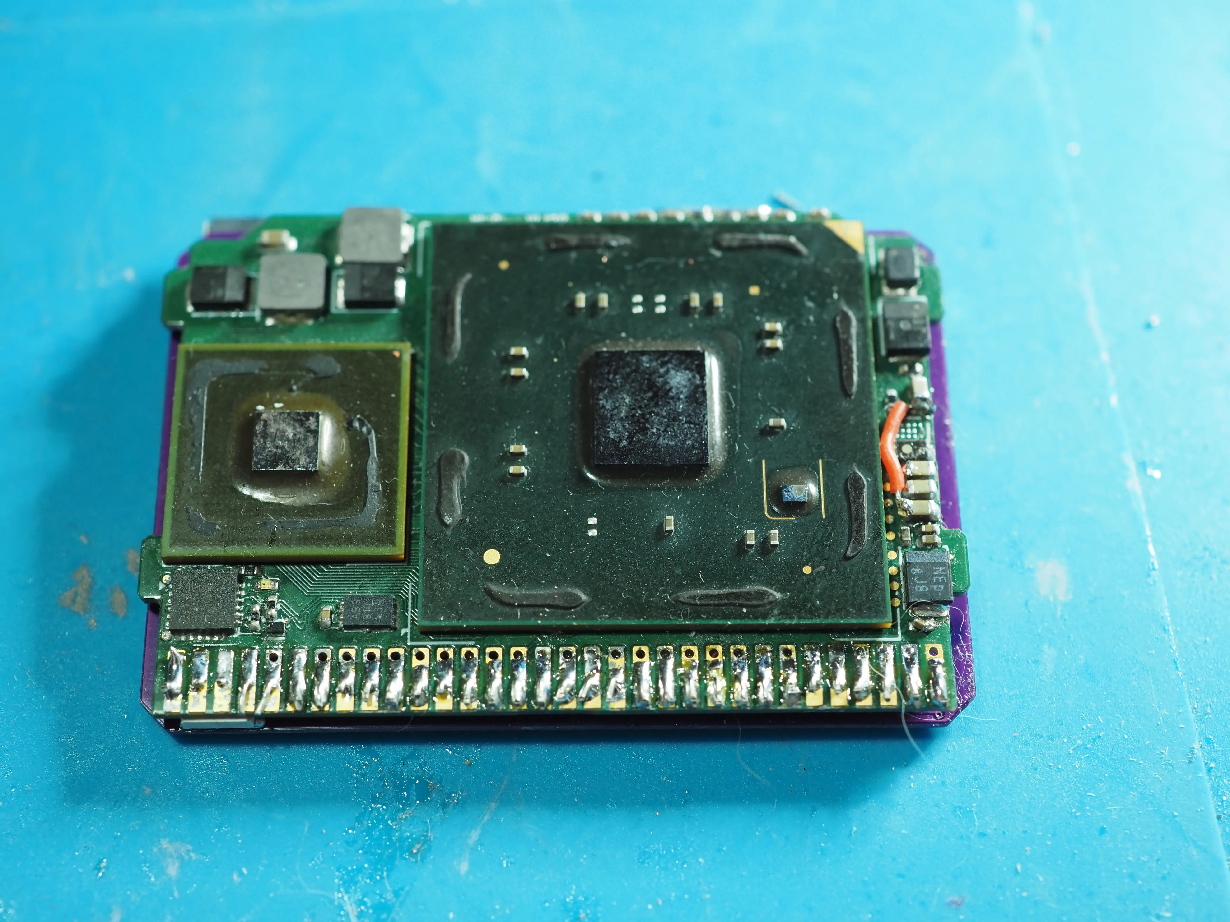
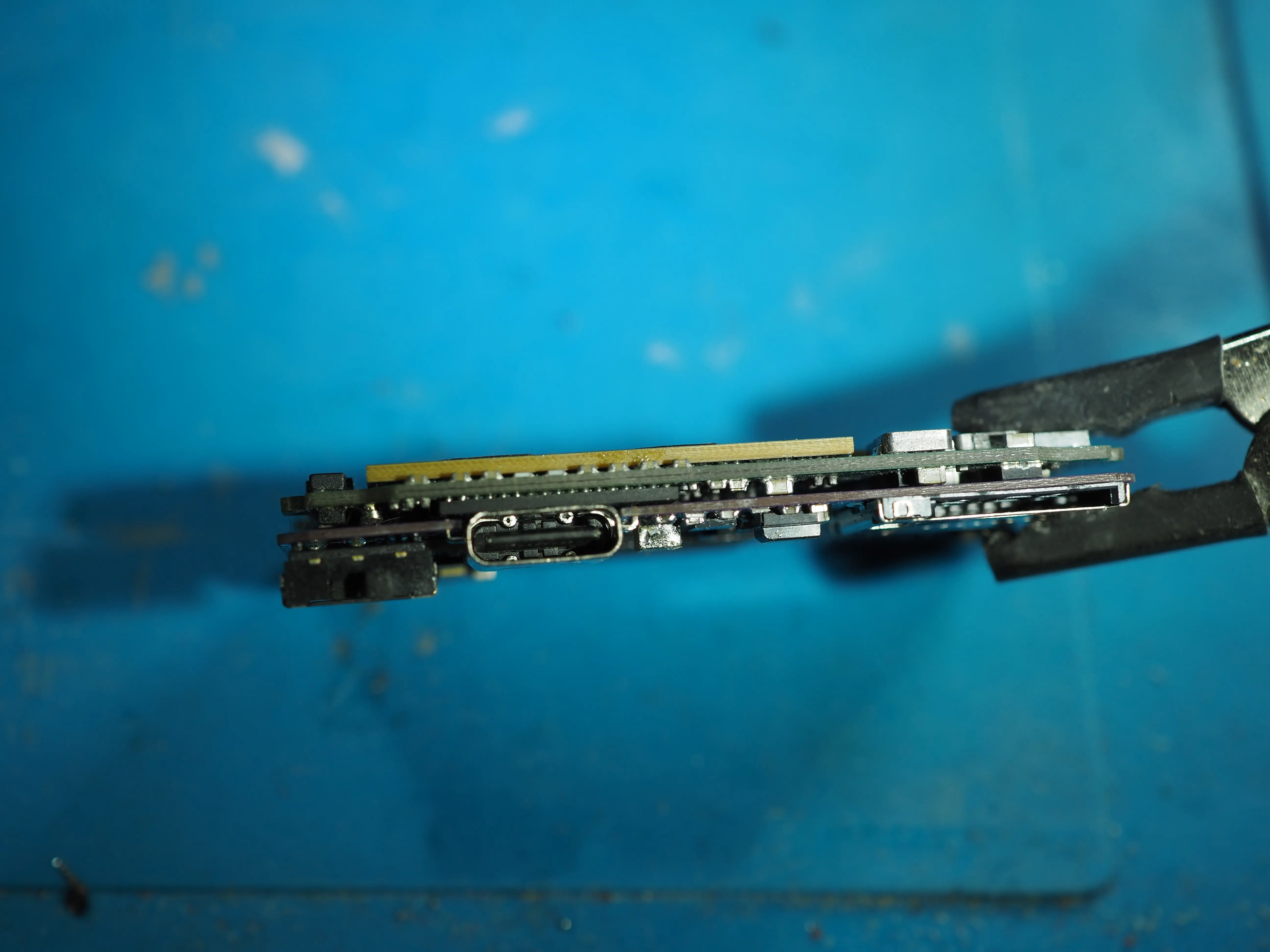
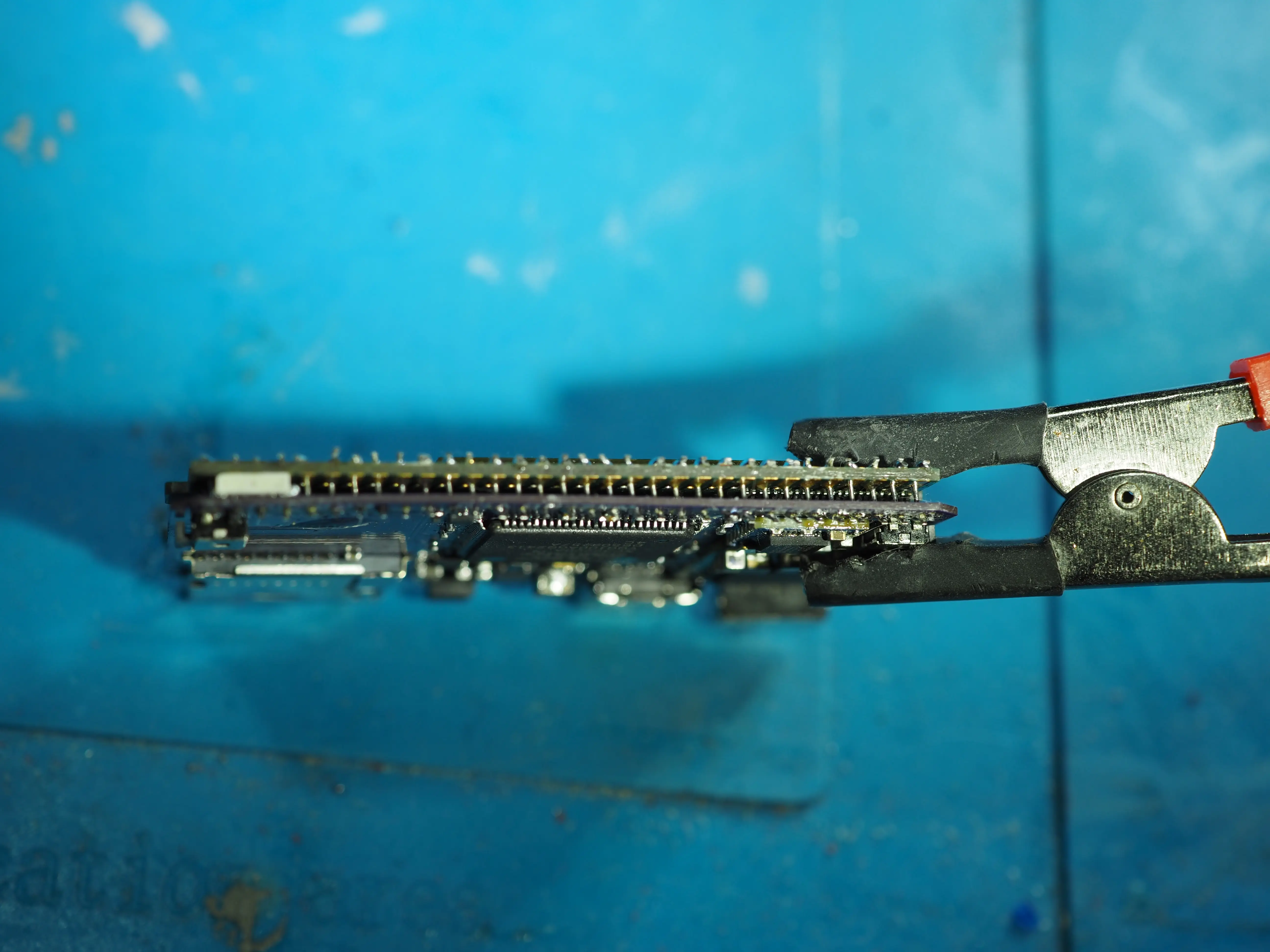
Before the final weekend
After the last proper update, I got a message from DHL that the Pico Pak was taken for clearance, and that I needed to supply proof of purchase. I did so, and the Pico Pak was released shortly after and arrived before the weekend
I love it, it fits together so well ^^ However there is one minor issue… It does not want to fully close with the Pico inserted… As it turned out, when JLC asked me to thicken the case, I moved the Z position of the Pico, but I forgot to check all clearances… And the ram now collides with this ledge
So, I grinded it away XP After which it closed as expected!
Now there was another few packages I were waiting on, including the package from Mouser, which contained the parts for the Zero, and the correct PIC for GC+ 2.0. I had ordered the components on September 14th, which should have been plenty of time… Right?...
The components arrived in Ireland on Wednesday the 16th but got held up by clearance.
On Monday the 21st the components left Shannon distribution centre. Yey it’s moving!
On Tuesday the 22nd the components left Shannon distribution centre. Hmm the previous one must have been a mistake.
On Wednesday the 23rd I got a call from FedEx saying my package containing *checks notes* “Ceramic capacitors?” was held up by clearance, and that I needed to supply proof of purchase.
On Thursday the 24th the components left Shannon distribution centre… I have a bad feeling about this…
I email them again, I need the components ASAP preferably before the weekend, but hear nothing…
On Friday the 25th the components left Shannon distribution centre… Oh no…
I went through Ask FedEx chat support and supplied the proof of purchase there as well… And a few hours later I hear back! The package has been cleared!!!
On Monday the 28th the components left Shannon distribution centre… Fuck!
On Monday the 28th the components arrived at the local FexEx facility! Wait it moved!
On Monday the 28th the components left on a FedEx vehicle for delivery!! It’s actually going for delivery!
On Monday the 28th the components arrived at my house!!! I’m out of purgatory!!!
I had 3 days to solder and test everything… Where did all that buffer time go? XP
I had one more package mishap, I ordered a Wavebird controller to use with the Zero. I ordered it on September 12th, it was supposed to arrive between September 22nd and October 2nd.
… And arrived at my place on October 5th… What the fuck is up with shipping?!
The final weekend, and 3D printer adventures…
It’s the final Friday, Friday the 25th. It’s the final weekend and I still have quite a few things to do. But with a full weekend I should have plenty of time. So, this was the basic plan of what was left:
- Check the fit for the Pico and the Riser, and that the contacts align.
- Boot the GBAWii4 and see if the Pico works in it.
- Check return voltages.
- Check video signals.
- Check that the GCVideo HDMI works
- Check that the HDMI mux works
- Do I get video over USB C DP?
- Do I get signals on the HDMI lanes for the internal display?
- Do final touches on case.
- Make the trigger buttons look nice.
- Make sure the moving heatsink works.
- Make sure controllers work.
- Do final prints of the case.
- Solder the screen HDMI wires and test the internal display.
- Do final assembly and solder in the final batteries.
- Solder up the Zero.
- Program the Zero.
- Test the Zero.
- Make a case for the Zero.
- Make the final worklog entry.
- Glory shots and final video.
It seems like a lot, but it should be doable as long as nothing goes too wrong… I have the whole weekend, and a short day on Wednesday, and I could always pull an all nighter if I need that last push. Though I’m to feel a bit iffy… But it’s fine, it’s just a cold, I’ll power through.
So on that Friday I did some more case work. And one package which did arrive was an Aliexpress order, which contained my new 0.2mm nozzle, which would allow me to do higher quality final prints!
I look up the instructions for changing the nozzle on my new K2 Pro. Unscrew the 0.4mm nozzle. And start screwing in the new nozzle. Hmmm, should it be that hard to tighten?... Let me unscrew it to check that I’m not cross threading the threads… Oh… Only half of the nozzle came back out… Well, that sucks… But if I screw it in again, it should line up and still work? Right? Getting the other piece out will be a future me problem… I tighten the nozzle again, but it gets fully stuck… But it has auto levelling based on the nozzle, and it’s just the final bit which didn’t go all the way in… Maybe it will work?
So, I turn on the printer, and make it extrude the filament… *Clunk* Oh the nozzle collides with the poop chute… Yeah no this is not good… Emergency shut down… And now it’s time to look up how to disassemble the whole hot end… yey, extra stuff I need to do…
Some disassembly later, and I have the piece which is stuck in the heat break… It’s really stuck and no amount of pliers can get it out… In the end I needed to do some percussive maintenance…
Note to self, don’t buy cheap nozzles from Aliexpress… The stock Creality nozzle is 4.75mm in diameter, the Ali special was 4.8 - 4.85mm making it just slightly to big to fit…
Also note to self, when something feels wrong. STOP, and don’t continue…
Anyway, I ordered an official Creality 0.2mm nozzle with next day delivery, and managed to fix the printer XP
Saturday, Sunday and Monday?
What had only been a cold on Friday, turned a lot worse on Saturday… It felt like a fever… But I still had stuff I needed to do! So, chugging some paracetamol, I tried to power through like planned. I can be sick later; this is more important!
First, I did some accounting, I had wanted to know how much this whole project had cost me, so I made a little spreadsheet. Note that the categories are a fluid, and there are parts which are under one category which are used other places as well. And the Shipping and Tax section is primarily for big ticket items like JLC and Digikey/Mouser. Smaller items from Aliexpress and Amazon has their shipping and tax included in their items.
So, I’ve spent about 1700€ on this project! Which is ~1900$, or ~1440£. So yeah, it’s not cheap XP
After procrastinating I needed to return to actually working on the project, though my headache and being generally properly sick had not gone away… It had actually gotten worse…
I took out the GBAWii4, slotted in the riser, then tried to boot it… Why is it not turning on?... I poke it with a multimeter, and it has power… I connect over UART… Nothing… Hmm, that’s odd, it was working a few weeks ago when I programmed it initially. But oh well, I’ll just reflash it and see what debug stuff I can add. Hmmm… The programmer can’t talk to the Tiny… Fuck, is it dead?!
I look around and find that I have one spare Tiny that is not being used. So I desolder the old one, and solder on the new one. And I can talk to it with the programmer! Yes! Oki lets see if it will run… No… Out with the multimeter… There is a short on SDA and none of the pins on Port B is reacting at all…
At this point I was feeling really ill, and ended up taking a break… Nothing was working, and I was too sick to think clearly… So a few hours break would not hurt right?
I didn’t do any more work on Saturday… And Sunday was worse… Though it started clearing up towards the end of the day… But I had still lost the weekend… Fuck I’m suddenly a lot lower on time than I expected…
Monday morning, I feel better, but decide to skip Uni. It gives me one day back where I can work sole on this!
I resolder the Tiny, and the Port B pins work again, it was just a bad solder joint on one side of the Tiny. But SDA is still shorted… I manage to trace it down to the riser. Without the riser the short goes away. With the riser installed, there is a shot on SDA to ground. And a short on 3.3V to ground. And Bluetooth Data + and – are shorted together… That is odd. But at the time I assume that the receptacle has an issue where the pins are slightly too big and it might cause the plastic between pins to break and short out. (That was wrong, but it was my assumption at the time XP )
I cut the neighbouring pins for all the shorted ones, I cut the ground next to SDA, and the ground next to 3.3V, and the two BT lines as I’m not using them, and it seems to work. SDA is no longer shorted, and the Tiny is reacting as it should. The GBAWii4 is alive again!
Now does the Pico work with the GBAWii4? Nope XP
I cannot boot while the Pico is inserted… And if I boot first then insert the Pico while the GBAWii4 is running, I end up seeing something weird… The battery rail, supplied by a power supply, drops quite a bit, and the Tiny stops responding properly… And I do sometimes get the 1.8V return voltage, but I don’t get the 3.3V I’m expecting, instead I get 0.6V…
I start by trying to eliminate what the issue is, by putting tape over the pins on the Pico.
Only connecting the power and ground? They are both happy!
Connecting I2C? Nope the Tiny stops responding. I assume they get stuck in a race condition of who is talking on the line… I’m low on time, and the I2C lines between the Pico and GBAWii4 are not critical. Cutting them would stop them from talking, so the GBAWii4 can’t get the temperature from the Pico, so I have to set a fixed fan speed. And the Pico can’t get the battery voltage and usage. But both of these features are optional, so cut it is XP
Oki it works better, but when I remove the tape on the 3.3V line, the voltage drops and the BMS and Tiny browns out…
I was still not 100% healthy, so I decided to leave it there, and started soldering the Zero instead XP Then I spent the rest of the Monday trying to figure out how the WavePhoenix firmware worked… While having a headache still… It was built on an older SDK than what I had, and it was causing issues…
Tuesday, I go to Uni, then come back tired… I think I did some final things on the case and started final prints. And kept poking the issues on the GBAWii4.
The final day
Wednesday, I have only one lecture in the morning, so I had the whole day to get something working, and as the deadline is 5am in my time zone, I got most of the night as well. XP Though I’ll will need to cut down on what plan to do, I need a minimum viable product. A worklog takes hours to write, so yeah that’s gonna be cut… But as long as I get the GBAWii4 working, that’s all that matters. And if I fix the 3.3V issues, it should just work…
Oki so how do I fix the 3.3V issues? When I connect the Pico, the 3.3V is only 0.6V, so there something funky going on. Now 0.6V does that not look like a diode voltage? Could it be that there is a short pin to some kind of voltage protection? I did have that voltage protection of VDD+0.5V on the Tiny, and this kinda smells like that.
Multimeter in diode mode, and sure enough I get 0.6V. So, there is something there! What’s the easiest way to find what components is causing the issue? Desoldering every component one by one! It might take time, but it is a sure fire way to find the issue!
What is on the 3.3V rail? The Audio decoder, MX, SD to USB bridge, FPGA for GCVideo, and the HDMI MUX. The FPGA is the worst one by far, so let’s take that one last.
Audio decoder removed, diode mode still reads 0.6V…
MX removed, 0.6V.
SD to USB bridge… 0.6V
HDMI MUX… Nope…
FPGA… Yeah, the issue went away… but fuck…
Soldered the FPGA back and… 0.6V… What?!
Wait am I being stupid? Let’s connect an external 3.3V voltage to the rail… And I get 3.3V… The 0.6V diode was never the issue! Fuck me!
Solder all the components back… And the external 3.3V still hold.
Okey, lets have a deeper look at this, lets probe the riser. Oh the 3.3V pin is Open Loop… The pin was not soldered properly… the 0.6V was back feeding voltage… Well that was a lot of wated time. But all I need to do is solder that contact right?
Let’s take a closer look at the riser, the 3.3V pin is the 7th pin from the left. 1, 2, 3, 4, 5, 6, 7… Hmmm that is odd, looking at the back of the riser… Pin 7 is ground? What? WAIT! Pin 2 and 3 which is the Bluetooth pins are connected together on the copper! That is the copper meant for VDD, which is pin 2 and 3 from the right! OMG I FLIPPED THE RISER!!!! ALL THE SHORTED PINS WERE BECAUSE THE RISER WAS SOLDERED IN REVERSE!!!!!!! SCL ended up where there was a ground pin, same with 3.3V, what is why I got a short on them, it was not the receptacle breaking, it was the god damn riser!
Okey, but that’s fixable, I just need a new riser. I’ll desolder the pogo pins as I don’t have backups, then I’ll solder them on the new riser after making triple sure the orientation is correct. The silk screen is on the wrong side, not sure why, and it does not matter now.
One set of extracted pogo pins later, and it’s time to solder them. Aaaaaaaaand there is solder on the wrong side and it’s bridging pins… Fuck! They are important pins! Double fuck!
Okey maybe if I use some solder braid I can wick it clean? First attempt… Nope, I just melted the plastic of the Pogo pins… Well I can just try again… Fuck I’m low on solder braid, I only have about 4 uses left… Let me check I think I have some more somewhere… Nope can’t find it… Maybe B&Q sells some? Yes they do! Wait this is the UK website, let me switch to Ireland to check if my local one has some… Nope B&Q Ireland does not sell solder braid/wick… Fuck… I have no clue if there is any other stores nearby which sells any, and I don’t have time to travel around and check…
Oki I got to make do with that I have… The soldering iron does not reach deep enough, so what if I just… Cut… The plastic? It’s not the cleanest solution, but it is a solution!
Some plastic shavings later, and it seems like the iron will fit in! Oki let’s take one of the remaining solder braid pieces I have and give it a shot! Aaaaaaaaaand it worked!!!! I managed to clear the solder bridge!!!! Whoop!
Alright, let’s plug the riser in, and see if it lines up with the Pico still…. Nope… It’s angled slightly too low, and won’t hit the targets… Damn… Lot’s of finicking later, and I found that if I pull the riser slightly out of the receptacle, it will line up. Maybe I can make a spacer? But that is a later me problem, for now let’s test!
The voltage drop is still there… And now the GBAWii4 freezes after plugging in the Pico… And checking voltages, it does turn on! I do get 3.3V now!!! But 1.8V only shows up sometimes… It seems the riser not being seated fully leads to a bad connection… But let’s at least check if it is running… The 54MHz video clock… Is 54MHz!!! The Pico is still booting and running!
Okey at this point fuck the riser, I’m tired of messing with it. I need the shell to support the Pico to make it aline with the riser, but that blocks me from poking most of the board, so I can’t find that voltage drop… It’s getting late and I’m out of time… Magnet wires worked before, so I guess I’ll just hard solder it… It won’t be pretty, but as long as I get it working, that is all that matters.
Time to disassemble the Pico, remove the pogo targets… Using two of my remaining solder braid lengths… And needing to fiddle with the holes to clear the last few…
Hmm, the pin pitch for the connector is 1.27mm, I’m sure I have some ribbon cable which is supposed to be 1.27mm pitch. That would likely look nicer than just going magnet wire. Oh, I found it!
Time to strip, twist, and tin 38 ribbon connectors. Then stick them into the Pico one by one and solder them… Ehm… That ended up taking a lot more time than I had planned… But oh well, it looks kinda cool, it’s like an IDE powered Wii now XP
Now let’s strip twist and tin 38 more connectors for the other side… At least I have some practice XP And I’m going to only solder a few of the connectors first, I want to know why the voltage drops, and if there is some specific pins which causes it.
I desoldered the pin header from the first riser, and soldered VDD and Ground.
Then connected the Pico… Please boot… Please boot… It boots! But there is still a voltage drop… Where the fuck does it loose 1V? There must be a high resistance somewhere… Is it the power switch to the pico? No… Is it the BMS? No… Hmm the voltage going to the battery pad is also low… What about the connector between the PSU and the GBAWii4? There the voltage is correct! Wait is it the wires between the connector and GBAWii4? Yes! Touching them and they are hot! I’m using to low of a gauge wire for the current going through it!
Okey, quick solution, what is the thickest wires I have? 16AWG? Yeah that should do it! Aaaaaand the voltage drop is gone! The brownout of the BMS and Tiny no longer happens! Problem solved! Maybe I can make it in time!
Let’s solder all the remaining wires to the Pico and test it! It turns on! Let’s check voltages. 1.8V? Check! 3.3V? No… What? Let’s check on the Pico side. Yes the 3.3V is there. Let’s check on the end of the ribbon cable… Yes 3.3V. On the underside of the GBAWii4 where the receptical is soldered? Nope… What? Okey let’s unplug the pins and check. It’s pin 7. 1, 2, 3, …, Wait pin 7 has been cut?!
Do you remember how I had some shorts on the riser early on, and I thought it was due to pins touching in the receptacle? And how I cut the adjacent ground pin that I though it was shorting to? Well turns out I can’t count, I cut 3.3V and SDA, not the ground pins next to them… XP
Okey it’s all coming together, it explains more of the issues I had, but for now, lets cut the pin header up, and solder the 3.3V pin onto a new pin.
I plug it in, aaaaaand it stops working… Fuck… and at this point it’s late into the night… I’m out of time…
If I unplug the 3.3V pin, it boots, and if I plug it in while it is going, it works. If I turn it off and on it work. But if I leave it off for a while and then turn it off, then it does not boot… Is there some kind of startup rush which kills the system?
Dumb solutions, I’ll take the Pico apart again, program the Tiny on it to have lots of long delays. How about a 1 second delay from the Tiny gets power, till it turns on the regulators? Then a 1 second delay from the regulators turn on till it releases reset on the Wii? That should have plenty of time, right?
I solder the programmer on, and try to program it… It does not work… Wait why is the programmer power light off? Why is the programmer really hot??? I unplug it and check my wires… I had gnd and vdd reversed… Fuck! Oki wires fixed. Let’s plug the programmer in… Why is the power light flickering?... Check resistance… VDD for the tiny and ground is short… Fuck…
Time to desolder… It’s the Tiny… Resoldering it and the short goes away! But the programmer can’t talk to it… Fuck did I kill the Tiny? I don’t have a backup…
Let’s check my old projects again, maybe I have a ATTiny1617 or 3217 somewhere? Oh found one! It’s from a project I will use in a few weeks, but that is a future me problem. Before I desolder it, let me check that I can program it… Nope, the programmer does not want to talk to it… Did I fry the programmer as well?
The only other programmer I have that can work is my Snap, but I would need to use MPLab, and I need to supply external power… Some finicking around later and I validated that the Snap could program the Tiny on the other project. And that it can’t program the Tiny on the Pico… Oh well… I need a new UDPI programmer, and a stockpile of Tiny1617, as I’ve killed 2 so far.
Some desoldering and resoldering later, and the borrowed tiny is on the Pico, and it has been flashed with the updated firmware. Let’s see if it works. It starts booting! Then after 2 seconds the power light turns off… Fuck! What! Why! It’s so late in the night, I only got ~2h left of the deadline, and I’m tired…
Hmm the 3.3V rail is active, and 1.8V… And the video clock. Wait it’s running! But it does not react to the power switch… Let’s check some things… Oh the SCL is stuck at 1.2V! Oh, the firmware gets stuck as it’s waiting for the I2C to be clear! Disconnecting 3.3V and it works, nothing is holding up the I2C lines. Connecting 3.3V and I2C stops working… What is connected to I2C which is driven by 3.3V? The audio decoder. Well that is not critical! Desoldered! Oh, it works now! The power switch can turn it on and off, the pico is giving out voltages, and the video clock is where it should be! Maybe I can still do this? I just need an image!
The fastest way to check if I have video is MelonHD, I just need to plug in the USB C display I have. Plugged in. WAIT!!! Unplug. I’m still using a power supply instead of batteries. I’m not sure how happy the power supply will be when the BMS is trying to charge it XP. Okey time to solder the actual batteries in! One battery needs it’s wire extended. Then it’s stripping, twisting and tinning them. Then soldering them. And the console is battery powered!
Okey let’s try again! USB C plugged in. The monitor registers something! It sees it as an option for KVM… It does not see it as a video input… Maybe a USB C to HDMI dongle will work? If I can find it?... I did not find it…
Oki MelonHD is out, I’m to tired to try and figure out why. But maybe the internal display works? I just need to solder the wires. I already soldered all the wires on the driver board, so I only need to do the final half… Damn these wires are small… And why are my hands shaking? God I’m tired… Okey that is one soldered… And two… And one of the wires on the driver board pulled loose… Yeah no… This will take too much time… There’s about an hour left of the competition… I don’t think there’s much more I can do… Fuck…
Okey back up. I have the Zero, I just need to solder the Pico Rev 1 to it, and it should just work. Then I can show that the Pico and Zero works. That was supposed to be the backup anyway, but the plan had been to solder and test the Zero during the weekend, but since the components didn’t arrive, it ended up being delayed. But maybe I can pull it off in this last hour?
Oki it’s all soldered up, let’s test it… Does it work?... No… Let’s poke around… I get voltage in, but the 3.3V regulator is not turning on… Fuck… I don’t have time to figure out why…
There is 30min left before the deadline… Oki let me put the GBAWii4 together as much as I can, and let’s make some videos at 04:30… Swapping over to final cases, and inserting all the buttons, lining the rubber domes up, screwing everything together… It’s 04:45 by the time I’m ready…
My flatmate sleeps in the room right next to mine, I don’t want to film and speak while he’s sleeping, so down to the living room, and using his desk as it’s a nice clear space. I don’t have time for retakes, so it’s now or never.
I film one video, then decide that I want a dissasabled version as well. So I go upstairs and get my tools to dissasable the GBAWii4, and film the second video… I go back upstairs, it’s 04:58, I can’t wait for the videos to upload to google photos and to download them again. Let’s grab a USB cable and transfer them over to my laptop. I message in the discord that the videos are done and that I’m uploading. Then grab the youtube links while the videos are still uploading, and put them in my worklog. 05:01… One minute past the deadline. But surely that is fine. I did it! I uploaded! Though I feel defeated as I could not get the GBAWii4 or the Zero to work…
There’s only 1 hour till my alarm is supposed to wake me, so there’s no point going to sleep, so I just sit there… I’ve spent months on this… Every free moment… Pushing through exhaustion… And sickness… I’ve delayed university assignments for this… I’ve spent almost two grand on this… And this is the culmination of everything I’ve done and worked so hard for…
There’s a notification in the discord, the voting poll is live. And I’m not on it… What? Fuck! What? Why? Is it cause I didn’t finish? No I’ve been on the poll before with unfinished projects, and there is a 20% bonus for completing you main objectives. Is it cause I was 1 minute late? Surely not… Let’s read the rules again… Oh I need to set the worklog as complete? I completely forgot about while sleep deprived… I switch the tag and ask in the discord what’s up… And yeah, apparently, it was not switching the tag to complete that did it… Fuck… I want to cry… That sucks so much… Everything was for nothing?... I should just have slept… Why did I do this?... God damn I’m stupid…
Some more chatter in the discord… And the moderators allowed me onto the poll as I had been right on the deadline! Whoop! That’s amazing! It wasn’t all for nothing!!! And I’ve learned a lesson in not uploading at the very last minute and making sure I triple check the rules after submitting XP
But seriously, thank you moderators for allowing me on the polls even though I delivered literally last minute.
After that I drove to university after having been awake for 24h, did my first class as it was a group project. Then left as I could not do math while that tired XP (PSA: don’t drive while sleep deprived! XP )
Getting home, I still had to stay awake till the night came around again…
But as I sat there, trying to not sleep, I kept thinking about this whole absurd project… This is 3/3 times that I’ve failed to deliver a working portable in the end. In 2021, I killed the BMS on the last night… In 2025 I ordered the PCBs too late, then they got delayed, and I got sick. I also had several issues that I would have caught had I ordered earlier and actually tested it. And now 2026, a riser being soldered in reverse, drove me to waste too much time before I figured it out. Along with getting sick again. Either I need to order things even earlier so that I can aim to complete my project way before they are due, or I need to accept that I suck at making handheld consoles XP I have plenty of other projects which turned out great and worked as intended, but making a portable seems to be the bane of me XP
Though I did have some stuff working. The Pico and test dock worked, I ordered that way earlier, tested it, and even got a second iteration through. Wait… Isn’t the Pico the more impressive accomplishment? And the Pico actually worked! Both rev 1 and rev 2! I reverse engineered the Wii GPU, CPU and what traces were needed. Made a spreadsheet of all the pins. And figured out how to put the RAM on the backside by moving the DQ groups around! It’s the smallest Wii motherboard ever made! And it fucking worked!!! The GBAWii4 and the Zero were only supposed to be docks which showed off the main accomplishment of the Pico. But as I got the Pico working months ago, I kinda forgot about it as I kept getting tunnel visioned on the GBAWii4 and Zero.
I managed to squeeze a custom Wii motherboard enough that it could fit inside a GBA Cartridge! And that’s kinda amazing XP So what if the docks didn’t finish in time, I made the fucking smallest Wii motherboard in the world!
And I’ll release the project files after I’ve cleaned them up. As I really want to see what the rest of you manage to do with the design! Will we see a Wii Femto? Will we see a Wii inside a Wiimote? Inside a phone? What kind of crazy things can you guys come up with when the smallest working Wii motherboard is just 31x49mm and that includes a ThunderVolt implementation! XP
Though that also leads into a few points. None of that would have been possible without this amazing community, and being able to use the knowledge built so far. YveltalGriffin for the ThunderVolt, Scampi, FujiFlex and MelonHD, all projects I borrowed form to make the Pico and GBAWii4. Loopj for the firmware for the ThunderVolt that I extended for the Pico, and for the WavePhoenix for the Zero. Auralio for GCPlus. B_Rob1 for the first (on the forum) Wii motherboard recreation, his project let me catch some pins I had gotten wrong and let me better label some of the pins on the GPU and CPU. And helped with tips on how to solder GPU and CPU. And a massive thanks to the whole community ^^
Anyway, that’s probably enough for this final update, so this is me signing off, and looking forward to seeing how the competition results turn out tomorrow ^^
Glory shots
Pico Pak
Pico Internals
GBAWii4 Shell
The GBAWii4 is not inside so the buttons and joysticks have no supports.
And the glass is scratched as I was checking that I could remove the paint. The screen is slightly larger than the glass frame, so I would have needed to scratch off some of it to make the whole screen visible.
GBAWii4 Internals
Wii Zero

What an incredible achievement and journey, you’re right the Wii Zero is a huge achievement in itself. You should be proud.

- Joined
- Jan 15, 2020
- Messages
- 66
- Likes
- 64
It has been incredible following your journey across the past few months! The amount of things that you overcame and the amount of things that ended up working despite the odds is incredible! Who would have thought the Wii cpu and gpu could be moved closer together and the ram could be flipped to the other side of the board. I really hope you continue this project, you're so close, and I am a believer in the WiiPico and associated peripherals!

- Joined
- Sep 11, 2025
- Messages
- 58
- Likes
- 14
- Portables
- 1
Next step is creating a ultra thin portable wii with this
Similar threads

- Replies
- 2
- Views
- 641
- Replies
- 2
- Views
- 492

- Replies
- 20
- Views
- 3K


