Question Trimmed Wii 1.8V shorted with GND

Link

.
Joined
Feb 24, 2024
Messages
5
Likes
0
TLDR : Trimmed Wii first worked, then after further soldering 1.8V found shorted with GND, couldn't find the root cause, please help.

Hi there, 2 weeks ago I've trimmed my first wii motherboard as an introduction of my Ashida journey.
Here is the obtained result :

20240309_113300.jpg 20240309_113319.jpg

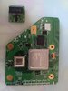
Then, after checking the resistance values between power and ground planes, which were as expected, I did the minimum connections with the RVL-PMS2 in order to check the boot, including the magnet wire dedicated to the U10 relocation.
At this point I had not received the Ashida batteries yet, so I sacrified an old GBA SP battery that still charges but does not withstand the load anymore. As expected, it did not whithstand the load at Wii power ON, so I also connected the PMS-PD power wires in order to get enough input power through the USB-C connector.
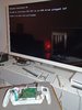
I also harvested the video output connector on the wii motherboard and connected a twisted pair of wires to the composite video pads.
I was so excited since my trimmed wii booted first try ! :D

20240309_233543.jpg

Unfortunately, I guess I spent my whole beginner's luck at this point: after that success, I decided to complete the connections between PMS-PD, RVL-PMS2, and trimmed Wii.
After a discouraging no boot, I got back to checking insulation between power and ground planes : I found a short between 1.8V and ground that I missed during the check before power ON. I know the expected resistance is quite low, but I clearly have a short here (less than 1ohm).

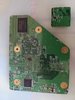
Since then, I progressively disconnected everything following my investigations. I can now confirm that the short circuit is unfortunately located on the trimmed Wii side. Despite cautious inspection, I could not find the root cause, so I removed every wire from the board, as well as the original big capacitor at C180 on which I had soldered the RVL-NTC, but the short is still there.
From the regulator picture in the wii trimming guide, 1.8V appears only in a few places, and it's easy to visually verify that both 1.8V and GND planes/tracks/vias are not connected by a mighty solder blob.

Now I have a few questions to the experts of Wii trimming :
  • Is there any chance that I damaged something within the Wii due to the power ON with the short between 1.8V and ground ? (It lasted a few seconds, just the time to aknowledge the no boot). Or could this particular short be a consequence of a wrong power ON ?
  • Is there an exhaustive schematics/illustration of the power planes / ground planes, and for both sides of the board ? I would like to be sure I investigated all possible locations for this short.
  • Could a 1.8V to ground short occur at the edge of the board ? Despite the first boot success, I did some extra sanding but it did nothing (each time I did some sanding, the sensitive chips were carefully masked and the board was IPA cleaned afterwards).
Many thanks in advance for your help !
 
Joined
Jan 27, 2023
Messages
80
Likes
40
Location
MX
Portables
2
First of all, congratulations for introducing you to the trimming world!! And with such a console as Ashida is

For your questions:
First you can remove EVERY component on the edges damaged by the trim, sometimes they cause shorts or malfunctioning

1- Did you use a heatsink or fan while you were testing your console turned on?

2,3- You can check for the Wii Compendium in this forum, using that you can see how the power and signals are distributed even between layers
If I’m not wrong, also there are some board scans with voltages on Shank’s Wii Super Thread, you can trace a line exactly where your trim is done and check if the edges have any 1.8V trace

Also I’m thinking but I’m not sure that you trimmed the board further than the trimming lines by watching your pictures (I think it’s only on the video port side), but this only can be confirmed by an expert on trimming. I see some damaged components that are safe on my trim, and it’s so close to the edges of the OMGWTF trim guide

Hope this can help you
 
Joined
May 24, 2018
Messages
51
Likes
60
Location
CHINA DALIAN
Friend, you can measure whether 3.3V is also short circuited to GND. The solder pads at the 1.8V voltage regulator are not clean enough, at least from the picture.
_20240325072941.jpg
 

Link

.
Joined
Feb 24, 2024
Messages
5
Likes
0
Thanks a lot for your feedback LCandell and ohkin86 !

First you can remove EVERY component on the edges damaged by the trim, sometimes they cause shorts or malfunctioning
Sure, I'll do that.

1- Did you use a heatsink or fan while you were testing your console turned on?
The heatsinks were in place (without thermal paste) but the fan was not connected yet the first time I powered ON and boot successfuly. The duration was only a few seconds so I do not believe I could damage the CPU.

2,3- You can check for the Wii Compendium in this forum, using that you can see how the power and signals are distributed even between layers
If I’m not wrong, also there are some board scans with voltages on Shank’s Wii Super Thread, you can trace a line exactly where your trim is done and check if the edges have any 1.8V trace
Thanks, it is exactly the kind of resources I was searching for, I'll be able to continue my investigations

Also I’m thinking but I’m not sure that you trimmed the board further than the trimming lines by watching your pictures (I think it’s only on the video port side)
I did that since I noticed that the Wii board could potentially clash with the Ashida batteries. Also, if you look to other trims that work, this video area is not critical, so I think I'm safe here, and it is proved by the first successful boot. But as you mentioned earlier, some edge components need to be removed.

Friend, you can measure whether 3.3V is also short circuited to GND. The solder pads at the 1.8V voltage regulator are not clean enough
Indeed, but I can confirm that there is no short of 3V3 vs GND and of 3V3 vs 1V8. Even pad 4 (maybe the most suspicious) behaves nominally : I have the expected resistance between pad 3 (1V8) and 4, and there is no short between pad 4 and 5 (GND) .

I keep you informed.
 

Stitches

2 and a Half Dollarydoos
Staff member
.
.
Joined
Feb 5, 2017
Messages
3,848
Likes
3,025
Location
Banana Bender Land, Australia
Portables
6
I gave the photos a good old patented Stitches Scrutiny™, but I can't see anything visually amiss that hasn't already been pointed out. The LDO footprint pads are a little rough (personally I'd run my iron over them to clean the jaggedy-ness), and there are a few components on the trim edge that have been damaged and should be removed, but afaik none of those things should cause a 1.8v to ground short, and definitely shouldn't cause a short after allowing one successful boot......

If you have a can of compressed air available, you could try giving the underside of the CPU/GPU a good blast from all angles to dislodge any fragments of conductive debris that may have found their way underneath. It might do the trick, otherwise I'm not really sure what else to suggest here.
 

Link

.
Joined
Feb 24, 2024
Messages
5
Likes
0
Thanks Stitches for your pattented inspection and additional feedback !

If you have a can of compressed air available, you could try giving the underside of the CPU/GPU a good blast from all angles to dislodge any fragments of conductive debris that may have found their way underneath.
I'll do that again as well. I masked during sanding but not during soldering, and you never know.

Meanwhile I started to analyze the board scan from Skank's Wii super thread, and I noticed 2 things (highlighted in dark red on the picture):

1V8_short_investigation_01.jpg

  • the C56 capacitor (red circle) is located between 1V8 and GND, and I've used the GND pad of the capacitor for my composite video wire. I can't see anything wrong here but I could remove this capacitor to check underneath. I already did it for C180 and found nothing wrong. Next to the 1V8 regulator, C4 and C5 are also concerned but I did not mess with them, so I don't intend to remove them for now.
  • I expect the red polygon to be 1V8 powered, but the scan shows that it is not part of the 1V8 plane, because there is already the 3V3 plane here. That means that this 1V8 red polygon is located on a track layer, and since the U4 regulator and C5 capacitor are on top side, I am convinced it is on the top layer. That means it is way closer from the ground plane (2nd top layer) than the usual distance between voltage and GND layers. The middle pad of the 1V8 regulator really does not look good: locally some board thickness along the edge of the pad is missing, so I wonder if I did not short the pad with the locally unprotected ground plane in my attempt to clean it, which I might have done between first boot and second failed attempt.
Since this 1V8 regulator is replaced by the RVL-PMS2, I think I'm safe to cut the track between the regulator's 3rd pad and the massive 1V8 pad on which we connect the PMS2, right ? I mean this track does not power anything critical other than R1 that is not required anymore once the regulator is removed, is that correct ?

EDIT : in the meantime I downloaded the compendium (incredible amount of work, congrats to the team and thanks a lot). It appears that I misplaced the C56 capacitor (red circle), it is between 3V3 and GND so forget my first point. I could also confirm that only R1 will be disconnected if I cut the track of the 3rd pad, so I'll go for it next, and keep you informed.
 
Last edited:

Link

.
Joined
Feb 24, 2024
Messages
5
Likes
0
Hey there, I progressed in my investigations, unfortunately the outcomes are not good:
  • blowing compressed air below the 1V8 related ICs (GPU, RAM, AVE) did not solve the issue.
  • after cleanly cutting the 3rd pad of the 1V8 regulator, the short remained. Ironically, the ugly pad was not grounded.
  • tantalum capacitors being sensitive to reverse polarisation, I removed C4 (C180 already done previously): capacitance measured as expected and short still there. Removing C5 did nothing more.
  • with nothing left to check on the top, I checked all related capacitors and resistors on the bottom: nothing suspicious visually. I won't remove all these tiny capacitors since I did not mess with them, so I assume visual inspection under magnification is enough.
  • I measured the following resistors, and found the expected values: R6, R11, R12, R14, R21, R23, R167
  • There was also what I expect to be a fuse, labelled "FIL4" : resistance measured below 1ohm, which seems nominal.
  • In the end I became paranoid and wondered if I could have applied too much temperature on the 1V8 regulator big pad when soldering the cable to the PMS 1V8. I mean in this area the 1V8 surface tracks are very close to the GND plane, so I imagined too high temperature could have done micro cracks in the thin insulation and some solder could have migrated between both planes. Lost for lost I cut the 1V8 large track after the regulator pad. Guess what ? the pad was not grounded, and the short is still there.
With no more clues left, I guess some connection was wrong during the 2nd power ON attempt and I internally damaged either the GPU either the RAM or the AVE. Do you think it is plausible ?
If so, this is by far exceeding my competences, so unless someone has another suggestion, I guess I should be happy that I learnt a lot and move on with my second trim...
 

Stitches

2 and a Half Dollarydoos
Staff member
.
.
Joined
Feb 5, 2017
Messages
3,848
Likes
3,025
Location
Banana Bender Land, Australia
Portables
6
That's about the limit of my competence as well. Sadly, sometimes trimmed Wiis just seem to die and there's no indication of why. Unless someone else knows some magic words, you'll probably need to trim a new Wii
 
Top