
VoxelTek
.
- Joined
- Apr 24, 2023
- Messages
- 8
- Likes
- 29
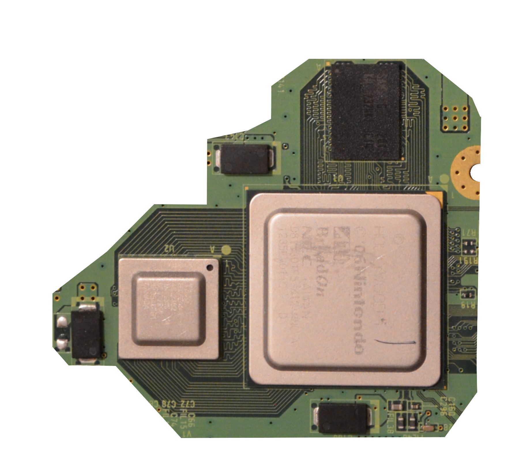
So my PSP-3000 kicked the bucket recently, much to my disappointment. (It may have been my fault, I am an idiot.) However, this prompted an idea: to put a Wii inside of the shell. At first I thought this would be an impossibly stupid idea, but then when I saw G-Man had done so a while ago, I figured I might as well take a crack at putting my own spin on the project.
Some of my main goals for this project are:
I originally intended to try and keep costs down as much as possible, and make my own PMS-type board. However, it quickly became apparent that I didn't have the resources and experience to make a PMS myself from scratch. At least, not without spending more than it would cost to just buy 4layer tech boards instead.
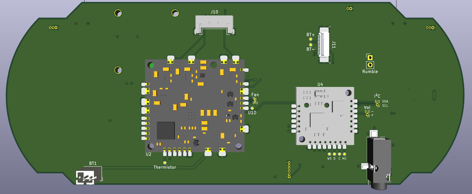
The PCB is made in KiCad, because I love FOSS and I'm a cheapskate Linux user. It's also the only thing I have experience with, and I wouldn't switch to another program even if I could. I want to put as much as I can on the PCB to avoid having to jerry-rig mounting solutions with hot glue and such.
As a separate project, I'd also been working on a flexible PCB for relocation of the "MX" chip on the Wii. That gave me a lot of experience with PCB design, and the project (and support I received from others on it) helped immensely.
Due to the small space, I figured an Omega trim was required. Given that Omega trims are hilariously unsupported, I started off by sketching up a rough trim guide for myself, based on a post on Twitter by BitBuilt.
Next, I got to work designing my custom PCB. Huge thanks to @Y2K, @YveltalGriffin and others for all their help and support during this process!
Strangely enough, I started out with designing a footprint for the PSP speakers. While I believe the original PSP-1000 uses connectors and cables, the 3000 uses "spring"-ed contacts on the speakers themselves. I took some measurements, made a to-scale test print on a piece of paper, and refined the footprint until it seemed it would work well.
With that done, I downloaded the 4layer board symbols and footprints, and then spent a bit of time adjusting them to fix errors and improve minor things. Following that, I began laying out some basic parts. and it was mostly just improvements and fixes until I got to where I am now.
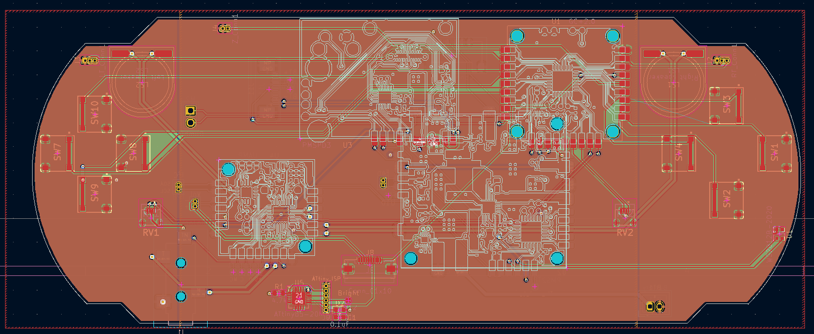

I intend to print out a scale paper copy of the PCB, to check for any major flaws, before I submit an order. The size of the PCB is larger than most, so JLC charges an extra fee for it, unfortunately. Given the price, I'd really like to get this as perfect as possible before ordering.
I really hope I can actually finish this project, and I hope it turns out as good as I'm envisioning. Thank you everyone for your assistance and support, I really appreciate it!
Some of my main goals for this project are:
- minimal external modification to PSP case
- minimal hot glue and other poor mounting methods
- maintains most of PSP appearance externally
- use of custom PCBs to help tie everything together
- as many bonus features (WiFi, BT, MX, etc) as possible
- project is somewhat reproducible
- portable contains batteries and is....well, portable
I originally intended to try and keep costs down as much as possible, and make my own PMS-type board. However, it quickly became apparent that I didn't have the resources and experience to make a PMS myself from scratch. At least, not without spending more than it would cost to just buy 4layer tech boards instead.
The PCB is made in KiCad, because I love FOSS and I'm a cheapskate Linux user. It's also the only thing I have experience with, and I wouldn't switch to another program even if I could. I want to put as much as I can on the PCB to avoid having to jerry-rig mounting solutions with hot glue and such.
As a separate project, I'd also been working on a flexible PCB for relocation of the "MX" chip on the Wii. That gave me a lot of experience with PCB design, and the project (and support I received from others on it) helped immensely.
Due to the small space, I figured an Omega trim was required. Given that Omega trims are hilariously unsupported, I started off by sketching up a rough trim guide for myself, based on a post on Twitter by BitBuilt.
Next, I got to work designing my custom PCB. Huge thanks to @Y2K, @YveltalGriffin and others for all their help and support during this process!
Strangely enough, I started out with designing a footprint for the PSP speakers. While I believe the original PSP-1000 uses connectors and cables, the 3000 uses "spring"-ed contacts on the speakers themselves. I took some measurements, made a to-scale test print on a piece of paper, and refined the footprint until it seemed it would work well.
With that done, I downloaded the 4layer board symbols and footprints, and then spent a bit of time adjusting them to fix errors and improve minor things. Following that, I began laying out some basic parts. and it was mostly just improvements and fixes until I got to where I am now.
I intend to print out a scale paper copy of the PCB, to check for any major flaws, before I submit an order. The size of the PCB is larger than most, so JLC charges an extra fee for it, unfortunately. Given the price, I'd really like to get this as perfect as possible before ordering.
I really hope I can actually finish this project, and I hope it turns out as good as I'm envisioning. Thank you everyone for your assistance and support, I really appreciate it!
Last edited:
")