Question Can these SNES JR consoles be repaired?

Joined
Feb 23, 2021
Messages
8
Likes
4
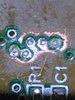
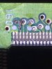
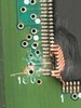
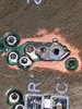
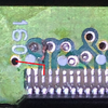
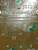
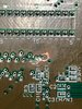
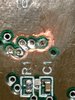
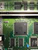
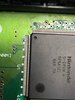
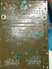
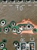
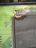
I was hoping someone might be able to provide some guidance on possibly repairing these SNES boards. So I have recently learned to solder and have been practicing quite a bit. I have been able to successfully install XenoGC mod chips into gamecubes, and thought an RGB amp installation would be rather simple and a good "next step". Both of these were purchased on eBay with the seller being fully transparent about them not working, but not to the extent of the condition they are in. Both are from botched RGB amp installs, on the 1st console (1-1 & 1-2) the pad is lifted from the CPUN chip pin, and the underside is missing a pad as well. The vias are filled with solder, I tried using a soldering wick to clear them but am unable to do so. On the 2nd console, (2-1 & 2-2) you can clearly see the scorched board, missing pins, pads, and traces. The underside is more of the same. I would imagine console 1 would be easier and more practical to repair, I just don't know how to go about getting the pad repaired, or if I would still be able to install an RGB amp, which is ultimately what I want to do. It was recommended to me to use bodge wires, for console 2, by running them to other traces/pads; and again with this one, I don't even know where to begin or which traces I would be able to run wires to. As far as equipment, I do have a microscope along with a yoctosun magnified headpiece. Are either either of these repairable, or should I just count my losses and buy a working SNES to RGB mod. Any help or guidance would be greatly appreciated
 

Attachments

  • SNES1-1.jpeg
    SNES1-1.jpeg
    768.2 KB · Views: 331
  • SNES1-2.jpeg
    SNES1-2.jpeg
    741.5 KB · Views: 364
  • SNES2-1.jpeg
    SNES2-1.jpeg
    723.1 KB · Views: 379
  • SNES2-2.jpeg
    SNES2-2.jpeg
    1.1 MB · Views: 348
It looks like it should be possible to fix as I believe it's only a dual layer pcb. Running wire in place of the damaged traces should be easy for the most part but soldering to that damaged chip will be very challenging.
 
It looks like it should be possible to fix as I believe it's only a dual layer pcb. Running wire in place of the damaged traces should be easy for the most part but soldering to that damaged chip will be very challenging.
How about the damaged pad on the 1st one? Should I rip the pad off? Should I just run a wire from the pin to the trace?
 
How about the damaged pad on the 1st one? Should I rip the pad off? Should I just run a wire from the pin to the trace?
If you're talking about this image I'd solder a new wire to the pin and run it through that via to the other side of the board and solder it to the non-damaged side of the via. Use a fiberglass pen to clean up the damaged area.
 

Attachments

  • Untitled.png
    Untitled.png
    1.1 MB · Views: 351
If you're talking about this image I'd solder a new wire to the pin and run it through that via to the other side of the board and solder it to the non-damaged side of the via. Use a fiberglass pen to clean up the damaged area.
Unfortunately, the underside of the damaged via is also missing it's pad, so as far as I know there's no other place to solder to, unless I can solder to another via that has it's pad, I'm just not sure if it would work.
 
Hopefully these are bit more clear. This is the first console console "A"
 

Attachments

  • SNES-A-BTM-1.jpeg
    SNES-A-BTM-1.jpeg
    1.8 MB · Views: 353
  • SNES-A-BTM-2.jpeg
    SNES-A-BTM-2.jpeg
    1.3 MB · Views: 338
  • SNES-A-BTM-CLOSE.jpeg
    SNES-A-BTM-CLOSE.jpeg
    904.8 KB · Views: 349
  • SNES-A-TOP-1.jpeg
    SNES-A-TOP-1.jpeg
    1.8 MB · Views: 396
  • SNES-A-TOP-2.jpeg
    SNES-A-TOP-2.jpeg
    1.2 MB · Views: 353
This is the second console, console "B"
 

Attachments

  • SNES-B-BTM-1.jpeg
    SNES-B-BTM-1.jpeg
    1.8 MB · Views: 334
  • SNES-B-BTM-2.jpeg
    SNES-B-BTM-2.jpeg
    839.5 KB · Views: 355
  • SNES-B-BTM-CLOSE.jpeg
    SNES-B-BTM-CLOSE.jpeg
    847.5 KB · Views: 326
  • SNES-B-TOP.jpeg
    SNES-B-TOP.jpeg
    864.7 KB · Views: 339

Attachments

  • Untitled.png
    Untitled.png
    3.2 MB · Views: 332
This is great!! Thank you for this!! Would I be able to just follow these scans for the severely damaged chip as well?
Yep, just take your time and follow where the traces lead. Just to be safe you should also try to run your wire a similar length to the trace as some functions may be strict on timing. (longer or shorter wire = faster or slower signal latency)
 
What neanderthal GRUG SMASH level PCB torture is this? Those poor Juniors..... I hope you can get them working again
 
Back
Top