Worklog WiiVision Build

Thanks. Since I have extra PMS PCBs, can I just solder the PIC to U6 on an empty board and power up with a battery to program the PIC?
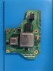
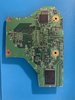
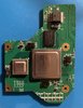
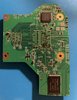
You could power the pic from the pickit. It wont work from battery because the BQ IC provides power to the pic. I think there is underlying problem here that needs to be resolved. Programing the pic on another pcb is not the solution.
 
I agree that there’s an underlying problem. I asked about another pcb to test to make sure that there’s nothing wrong with my PICKit3 and cable. So if the BQ IC is not supplying power to the PIC, then that could cause the target device not found (could not detect target voltage VDD) error?
 
A quick update. I was able to program a spare PIC on an empty PMS board using power from the PICKit. So my PICKit and cable are working. When I tested various pads on the PMS, I get -217 mv on the 3.3v pad, -170mv on the 5v pad, -247mv on the 1.8v pad, .9mv on the 1.15v pad, and -203mv on the 1v pad. For those of you who are experienced with the PMS board, does the negative voltages help indicate where the soldering problems may be?
 
There will be no voltage on the regulators until atleast the pic is programmed and you turn on the PMS with the button, it is normal. Measure the VSYS voltage, it can be found in many places like the large inductor and vsys is labeled there. If there is vsys voltage, then this is what powers the pic.
 
Thanks. The vsys voltage should be the same as the raw battery voltage, ~3.7v?
 
Thanks. The vsys voltage should be the same as the raw battery voltage, ~3.7v?
Yeah it will be close enough. Mostly concerned is there voltage or no voltage.
 
Of the two boards that I soldered. One has no vsys voltage and one has a fluctuating vsys voltage from 350 mv to 380 mv.
 
Of the two boards that I soldered. One has no vsys voltage and one has a fluctuating vsys voltage from 350 mv to 380 mv.
That's soldering problem. All the qfn pads of every chip need to have visible solder connection to the pcb. Make sure vsys is not shorting to ground either.
 
Thanks for taking the time to help. I think I may have reached the limit of my soldering ability. I used my rework station to remove and resolder various qfns but I still could not get the proper vsys. I guess I’ll just wait until the pms comes back in the store. Maybe with a working pms in hand I might be able to do some comparison debugging.
 
I decided to do some more debugging. When I removed L6 from the board then all the vsys pads are reading the battery voltage (~3.6). And when I tried the PICKit3, it can communicate with the PIC. I’m not sure what this means or if it helps to pinpoint the problem but thought I’d share it with the group.
 
I finally trimmed my Wii motherboard and I’m afraid that I might have damaged the board in the process. What’s the quickest way to verify that the board is working, or not working?
 
Here are the resistance measures.

GND -> 1V: 4.2 Ohm
GND1 -> 3.3V: 7.6kOhm; GND2 -> 3.3v: 2.6kOhm
GND -> 1.15: 3.4 Ohm

Here are the photos. Thanks.
 

Attachments

  • IMG_1473.JPG
    IMG_1473.JPG
    1.4 MB · Views: 410
  • IMG_1474.JPG
    IMG_1474.JPG
    1.6 MB · Views: 428
Last edited:
A couple things I'm noticing:

- The edges of the board look fairly rough, which is probably why you've got shorts on your 1v and 1.15v lines. More sanding is definitely needed
-I'm also concerned about the nick on the RAM. If there's copper exposed, then it's possible that the RAM is damaged, which may mean this trim is dead
 
Thanks. I had a spare Wii so I went ahead and trimmed it. This time I made sure that I did not nick anything. I have sanded the edges down using the 800 grit sandpaper. When measuring voltage, I get 307 Ohm GND->1v; 31 Ohm GND->1.15v; and 0.8 Ohm GND->3.3v. It looks like I have a short on the 3.3v but I have sanded the edges repeatedly but still could not get rid of the short. Also, I don't see a 1.8v pad in the voltage photo of the definitive trimming guide. Any suggestions for how to eliminate the short on the 3.3v is much appreciated.
 

Attachments

  • IMG_1481.jpg
    IMG_1481.jpg
    1.9 MB · Views: 408
  • IMG_1482.jpg
    IMG_1482.jpg
    2.6 MB · Views: 401
  • IMG_1483.jpg
    IMG_1483.jpg
    981.6 KB · Views: 431
  • IMG_1484.jpg
    IMG_1484.jpg
    862.4 KB · Views: 418
I sanded the edges down further using 1000 grit but I still can’t eliminate the short on 3.3v. I haven’t done the U10 relocation yet, would that affect the resistance for 3.3v? Is there a particular edge that I should focus on. Looking at the voltage layer diagram in the compendium, it looks like the top and left edges (when looking from the top) are where the 3.3v traces are. In any case, I’m stuck. So any suggestion is appreciated.
 
I suspect that I might have over-trimmed the board. Can someone tell me the component in the red oval is needed for the trimmed board to work? Thanks. IMG_1482 annotated.jpg
 
It looks like I’m moving onto my third trim attempt. This time I have a black Wii without GC controller ports. How do I complete soft modding without a GC controller?
 
It looks like I’m moving onto my third trim attempt. This time I have a black Wii without GC controller ports. How do I complete soft modding without a GC controller?
You can do it all with the Wiimote
 
Back
Top