- Joined
- Nov 25, 2022
- Messages
- 89
- Likes
- 15
- Portables
- 1
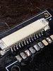
Thanks! Sorry if I’m asking too many questions I just have so many - by the looks of this photo, does it look like these pins are properly soldered? Is there a way to test before assembly ?
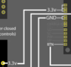
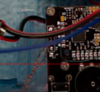
The PMS boards have multiple output pads for each voltage for convenience. That way you don't have to solder 5 supply wires to 1 pad to feed everything. The diagram is showing that any of the 3 pads is fine to use.Hello again! I have another couple questions. SO first of all I see in the wiring diagrams that some of the wires look like they lead to multiple pads or connections. I attached a photo for example (3.3v). Do I need to solder wire leading from 3.3v to each of those pads? ---- My next question is kind of a follow up to that, I saw gingerofoz build this and he twisted some magnet wire together but its hard to see where he wired it to. I attached a picture from his stream for an example. Is this to accomplish my first question or is this something else?
Thanks again!
No worries man. Better to ask lots of questions than make lots of mistakes in ignorance.Hellooooo once again, so all of the pcb boards are assembled and looking good! Also my wii is already prepared as I purchased it from crazygadgetmods on Etsy.
I am about to start wiring everything together, I will be using the diagrams on 4layertech's website to guide me. ---My question is, are the diagrams provided on their website going to show me everything I need?
Also I have not been able to find much help on how to wire up the screen driver board. So I have a couple questions with it
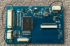
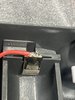
1. I assume I need to remove the circled components right? (attached photo)
2. Where do I wire those pads to?
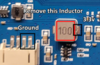
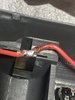
3. It mentions on 4layertech - "modded to power on 3.3v by removing an inductor and wiring 3.3v and ground." I see what it is talking about, but I don't know where to wire 3.3v and ground. (other attached photo)
Thank you again (stiches most likely). You gotta let me know if I start to annoy you with these questions lol I swear I am doing reaserch there is just so much to know.
The diagrams I am referring to - https://4layertech.com/products/ashida-pcb-set

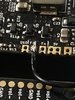
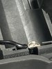
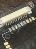
First joint looks a tad cold, but that might be because of the extra exposed wire poking out the end. Aside from that it looks good, but I'd definitely snip off the bit of wire that's poking out of the joint on the PMS for safety
That should be simple, I believe all you have to do is wire the switches to different pads. For left Z as a start button, you cut the trace going from the left Z footprint to the GC+, then run a wire from the Start pad on the GC+ to the left Z tact switch.Hey I also saw that gingerofoz made the left z button the start button and used the bottom two buttons for menu and up I believe. That way he could have some screen controls. Do you know how I would do this as well?