Worklog TinyTendo - an absurd NES handheld

Joined
Nov 4, 2019
Messages
26
Likes
207
Well I've never done a worklog before but the great Shank demanded I do one so here we are.

TinyTendo is my admittedly overly ambitious attempt at making a NES handheld in an original GameBoy form factor, which breaks conventions on how small a real NES can get.
unknown-46 (1).png

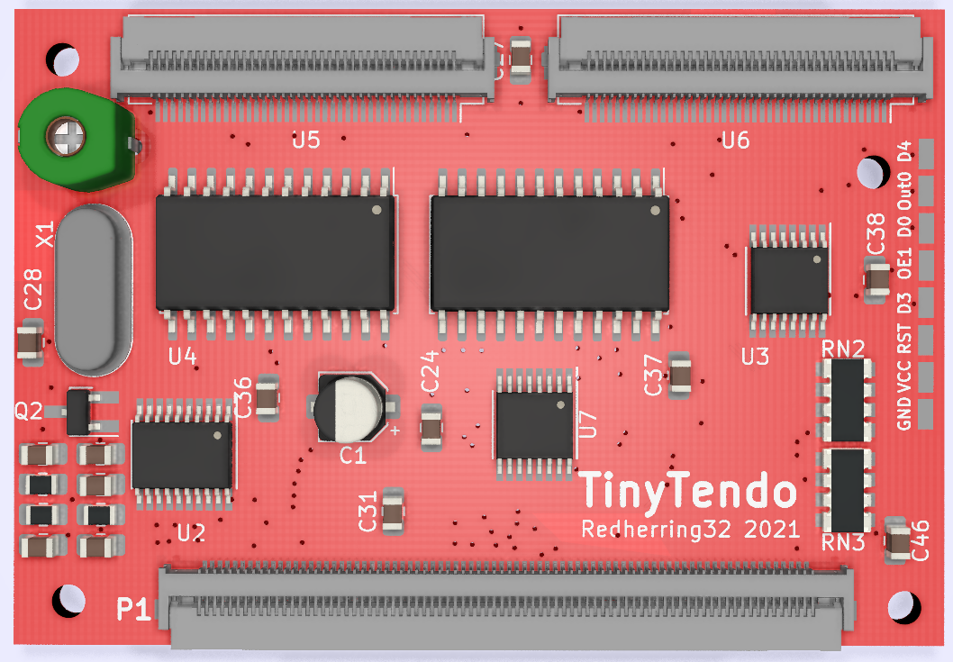
TinyTendo will utilize a custom motherboard, the current motherboard prototype features 3 FFC connectors for attaching the CPU, PPU, and cartridge slot, however I intend to move towards having these parts integrated into the final board.

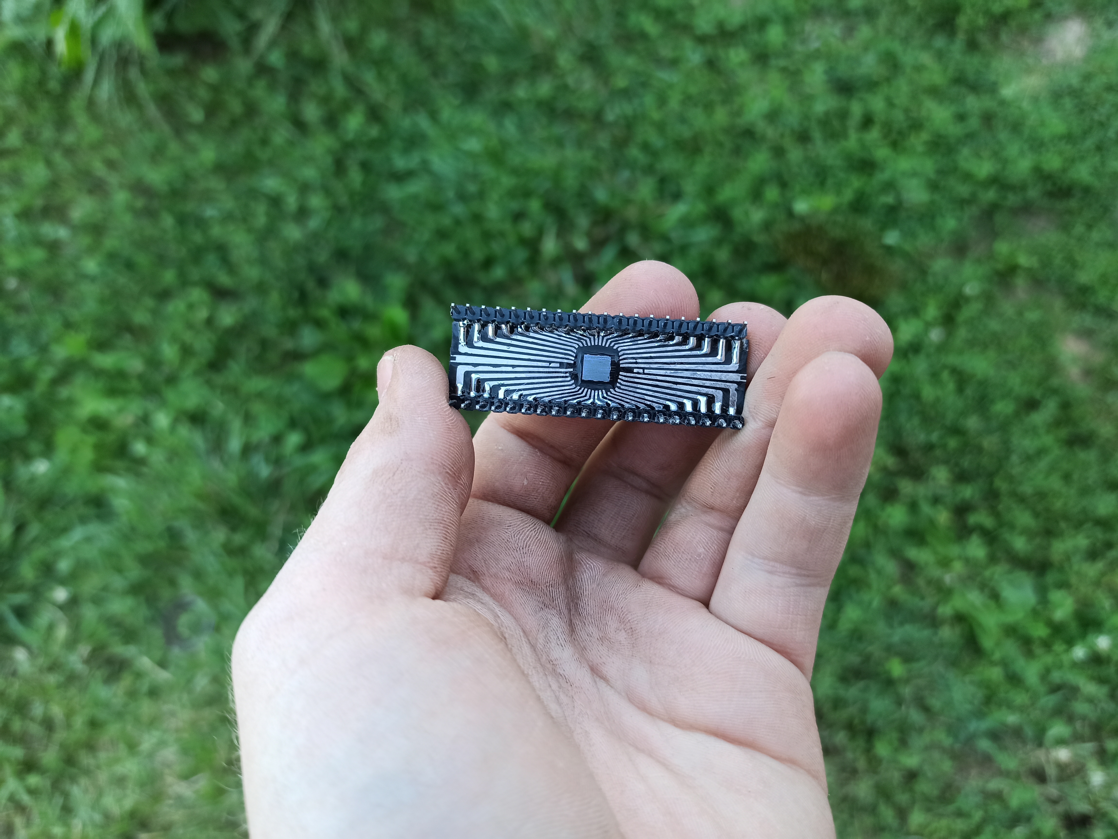
Now you may be wondering how I will be handling the CPU and PPU; the bottom of each chip will be ground down in order to expose the leadframe, and make the die flush with the leadframe:

IMG_20210616_185230.jpg


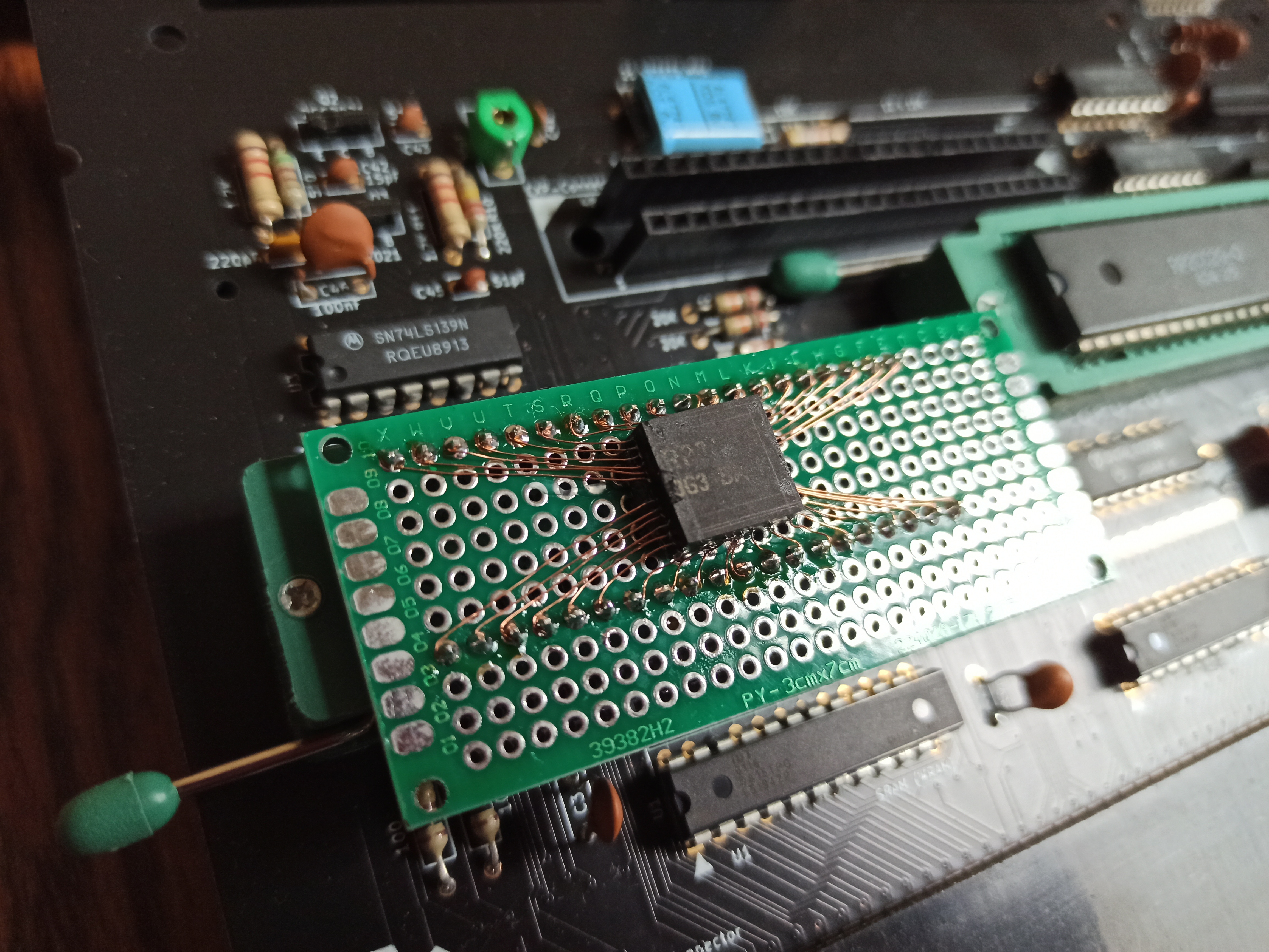
And then they will be cut down to a final horizontal footprint of 10x10mm in order to minimize the space they take up on the PCB:


IMG_20210227_123125.jpg


(The above image is of me testing if the cut chip still worked, and does not reflect how they will be used in the final design)

This process not only reduces their overall size, but also allows them to be perfectly surface mounted, and is what makes this project feasible.
If anyone would like me to go more indepth into how I do this, and how it's possible, let me know!

Anyway, I will try and keep this thread updated as I go, though progress will likely be slow. :)
 
Last edited:
Joined
Jun 2, 2020
Messages
30
Likes
23
Well, there's the CPU and PPU explained... DIP surgery is magic to my ape brain, lol. But how are you planning on doing NES carts on a portable with the form factor of a gameboy?
 
Joined
Nov 4, 2019
Messages
26
Likes
207
Well, there's the CPU and PPU explained... DIP surgery is magic to my ape brain, lol. But how are you planning on doing NES carts on a portable with the form factor of a gameboy?
I will be using a 0.8mm pitch 80 pin edge connector which will allow me to make compact custom cartridges.

It's maybe not elegant, but all of the more common mappers will compress down quite well, which is fine cause they're all I can afford. :)
 
Joined
Nov 4, 2019
Messages
26
Likes
207
Been making slow progress, but I have commenced work on the shell design.
Fusion360_lpOFRYVczI.png
Fusion360_BNUzwjULfC.png
IMG_20210701_214631.jpg
 

thedrew

.
.
Joined
Sep 27, 2016
Messages
444
Likes
1,004
Whoa this is genius. Love the idea of cutting down the original chips and making then essentially smd chips.

This process not only reduces their overall size, but also allows them to be perfectly surface mounted, and is what makes this project feasible.
If anyone would like me to go more indepth into how I do this, and how it's possible, let me know!
I'd be curious to know how you did it!
 
Joined
Nov 4, 2019
Messages
26
Likes
207
Hey guys!
Been a long time since I posted an update, mostly cause I'm just bad at keeping up with this stuff.

Anyway I wanted to share the large amount of progress I have made since the last post!

The motherboard has seen a redesign to incorporate the CPU and PPU directly on the PCB, as well as add audio mixing to it:
unknown-125.png

The DIP40 chip in the render represents what size the CPU and PPU normally are compared to the motherboard!

I have also made a significant amount of progress on the shell design, and it is now to my knowledge almost entirely done:
unknown-191.png
unknown-130.png
unknown-175.png

unknown-133-3.png
unknown-152-1.png


I never seriously modeled anything before this, and it probably shows :) but I think I did alright all things considered. (The final render is courtesy of @Wesk )

And last but not least, I finally got it to boot, too!

IMG_20211004_010057-1.jpg


I have also been working on something to show the chip trimming process, but that won't be ready for a little while.

Lemme know what you guys think!
 

Stitches

2 and a Half Dollarydoos
Staff member
.
.
.
Joined
Feb 5, 2017
Messages
4,069
Likes
3,189
Location
Banana Bender Land, Australia
Portables
6
Hey guys!
Been a long time since I posted an update, mostly cause I'm just bad at keeping up with this stuff.

Anyway I wanted to share the large amount of progress I have made since the last post!

The motherboard has seen a redesign to incorporate the CPU and PPU directly on the PCB, as well as add audio mixing to it:
View attachment 20024
The DIP40 chip in the render represents what size the CPU and PPU normally are compared to the motherboard!

I have also made a significant amount of progress on the shell design, and it is now to my knowledge almost entirely done:
View attachment 20025View attachment 20026View attachment 20027
View attachment 20028View attachment 20029

I never seriously modeled anything before this, and it probably shows :) but I think I did alright all things considered. (The final render is courtesy of @Wesk )

And last but not least, I finally got it to boot, too!

View attachment 20031


I have also been working on something to show the chip trimming process, but that won't be ready for a little while.

Lemme know what you guys think!
this pleases the nut.jpg
 
Joined
Aug 8, 2020
Messages
15
Likes
3
Crystal oscillator is available in 3225 package.

Can you share the package after CPU and PPU cutting?qfn?

[MOD EDIT - Don't double post]
 
Last edited by a moderator:
Joined
Nov 4, 2019
Messages
26
Likes
207
Crystal oscillator is available in 3225 package.

Can you share the package after CPU and PPU cutting?qfn?

[MOD EDIT - Don't double post]
The cut chips don't mount to any standard package footprint, the footprint is one I designed for the purpose.

Here's what it looks like:
unknown-88.png


And here's the leadframe of the chip that mounts to it:
IMG_20211121_003212.jpg
 
Last edited:
Joined
Nov 4, 2019
Messages
26
Likes
207
Just wanted to share a little update, finished a successful test print/fit, and *almost* everything fits perfectly first try.
IMG_20211211_152004.jpg


Just got some more testing/assembly to do on the charge/boost PCB, and 1 more revision on the main motherboard, then we hopefully should be set.
I did fry my CPU with an accidental short circuit, so I gotta trim another, whoops!

I also worked with someone to get the first cartridge mapper designed, isn't it cute?
IMG_20211209_144226.jpg


Will try and post more soon!
 
Joined
Nov 4, 2019
Messages
26
Likes
207
How to modify the video output and audio output?
The audio and video signals are amplified and sent to the speaker and screen respectively.
Other than amplifying the original signals, I'm not doing anything to them.
 
Joined
Nov 4, 2019
Messages
26
Likes
207
Hey guys!

While I've not been able to devote much time to the project lately, I have been chipping away at the smaller stuff.

If you've seen my 8bit power reduction thread, you will probably have figured out I'm looking into undervolting the NES hardware down to 3.3V to significantly increase the battery life of my handheld.
Now while simple in theory/on paper this has brought with it some complexities that need figured out.

Among the main things that need figured out to pull off undervolting the NES hardware are:

1) Whether all features of the chipset still work, and work exactly as they should.

2) Whether or not different cartridge hardware (Such as mapper chips) will behave as well at 3V3 as the NES hardware does.

3) Whether there is any benefit, or disadvantage to undervolting one revision chipset over another.

4) Whether NES peripherals/accessories such as the different controllers, 4 player adapters, or even stuff such as R.O.B work as they should.

I have been hard at work testing these things to the best of my current ability, but there's still a bunch more to do.
While my initial voltage/power draw testing data does prove the concept, it only applies to revision G chips, and may not hold true on the other (albeit less common) revisions.
I have started testing on a rev E chipset, and so far it seems that they aren't able to be undervolted as much as rev G.

In my testing of rev G chips, I pretty consistently got the CPU to crash at 3V, and it would run properly anywhere from 3.1-5V.
Rev E however I have found to crash at 3.4V, and only operate properly at 3.5V and higher.
There is a caveat though, as rev E appears to use less power at the same voltages than rev G does!

This sounds like an obvious choice at face value, use rev E chips, and get further battery economy.
However, the fact that they do not run at a standard 3.3V voltage means that my power management solution would need to be a bit more complex.

In any case, there's still a lot more to learn, and a lot more to figure out before I can implement undervolting in my design with any certainty.


As a little bonus, I wanna show something I whipped up purely out of curiosity as to whether I could:
unknown-176-1.png
unknown-99-1.png

A NES motherboard the size of a Raspberry Pi Zero!

Anyway, catch ya later!
 
Top