JBmodz
.
- Joined
- Mar 9, 2025
- Messages
- 96
- Likes
- 51
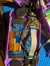
Big update: I have made alot of progress since my last update. I was able to wire up and test my trim, and it boots! Booting was unreliable, I assume because of my wire length, but I will rewire the voltage lines for final assembly. I installed the pms and some of the other boards in the case and wired the batteries to the pms. I put the screen and buttons in to see how it would look, gotta say I love how it looks with these translucent purple buttons and sticks! I also did the 3.3v mod on the driver board. Next step is going to be wiring up audio, VGA, usb , and the controller.
![IMG_20260407_200546[1].webp](https://bitbuilt.net/forums/attachments/img_20260407_200546-1-webp.42344/ "IMG_20260407_200546[1].webp")
![IMG_20260407_200626[1].webp](https://bitbuilt.net/forums/attachments/img_20260407_200626-1-webp.42345/ "IMG_20260407_200626[1].webp")
![IMG_20260410_193245[1].webp](https://bitbuilt.net/forums/attachments/img_20260410_193245-1-webp.42346/ "IMG_20260410_193245[1].webp")
![IMG_20260410_193251[1].webp](https://bitbuilt.net/forums/attachments/img_20260410_193251-1-webp.42347/ "IMG_20260410_193251[1].webp")
![IMG_20260410_193303[1].webp](https://bitbuilt.net/forums/attachments/img_20260410_193303-1-webp.42348/ "IMG_20260410_193303[1].webp")
![IMG_20260410_193310[1].webp](https://bitbuilt.net/forums/attachments/img_20260410_193310-1-webp.42349/ "IMG_20260410_193310[1].webp")