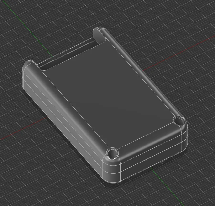
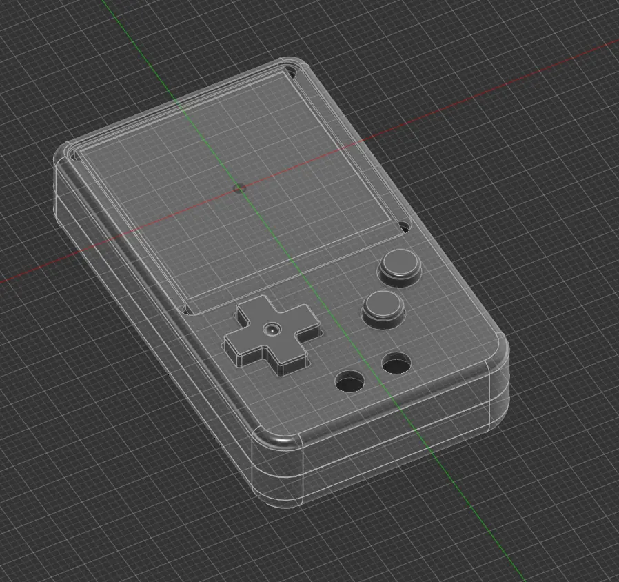
Despite my lack of worklog entries over the last 3 months, things have been rolling right along. However, because of the large amount of information there is to go over, I'll be splitting up the updates by workstream over the next few days. Today, I'll be going over the electronics.
EBC-LCD-DEV1
Picking up where I left off in the previous update, I'll briefly discuss the EBC-LCD-DEV1 board. In short: it worked. There was very little drama with the actual hardware, beyond an error in the LCD datasheet -- pin 15 was marked as D/C for the SPI interface, but it's actually pin 16. A quick bodge had things up and running pretty quick.
The software side of the LCD driver ended up being an absolute shit show. TL;DR: this LCD does not support the SPI clocks necessary to hit the bandwidth requirements for a 2x scaled GBC image, and in some cases you can't always trust the SPI clock you think you're at. However, I'll save most of that story for the next update.
EBC-CPU-X1: Schematic
With the hardware side of the LCD driver proven out, I moved on to the schematic and layout for the integrated EBC motherboard, designated EBC-CPU-X1 -- in keeping with Nintendo naming conventions.
The actual schematic design was a pretty simple affair. This is, after all, my 4th custom GBC motherboard design, so I have a solid understanding of that side of things. And because I had already designed a separate dev board for the LCD driver that interfaced with a GBC, it was just a matter of smushing the two schematics together, and directly routing all of the display signal lines from the GBC CPU to the RP2040 instead of through connectors.
The net-new pieces of the design are power, charging, and audio.
For power, I needed to generate 5 different voltages:
5V -> GBC IO
3.3V -> GBC core and RP2040 IO
1.1V -> RP2040 core voltage
1.8V and 2.8V -> Required by the LCD for reasons I'm not privy to.
You might notice that I've chosen to implement an external 1.1V source for the RP2040 using a boost converter, in contrast to most RP2040 designs I've seen, which simply rely on the MCU's integrated 1.1V LDO. For a larger device, or one that's intended to remain plugged in, I wouldn't have bothered. But because the EBC can only fit a small battery with a capacity of ~200mAh -- and because the RP2040 cores will be constantly working -- I wanted to ensure that it was as efficient as possible.
Charging is handled via my beloved BQ24072, which is a linear charge IC from TI. The nice part is that it integrates power path management, so system power is automatically switched between battery and USB VBUS when a charging cable is plugged in.
Audio is a very simple affair. All Game Boys support stereo audio, but because there's only room for one speaker, and none for a headphone jack, the two channels are simply ran through their own DC block cap and resistor before getting merged at the audio input of the amp. No room for my beloved and totally non-controversial volume wheel, so volume control is handled via PWM from the MCU.
Not shown, but I also added PWM brightness control for the backlight -- also from the MCU -- as well as a voltage divider that halves VCC(battery voltage) and connects it to a GPIO on the RP2040 for a software battery indicator(TBD).
EBC-CPU-X1: Layout and Routing
I'm the wrong person to discuss PCB layout in any detailed or meaningful sense, but this was where most of the effort went with this board. It's a 4-layer 0.8mm board, and holy shit, layout and routing was a nightmare.
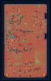
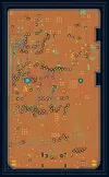
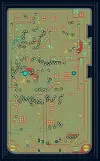
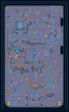
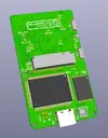
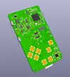
In hindsight, I would have had a much easier time if I had gone with a 6-layer board and just sucked up the added cost. While I tried to keep by internal power and ground layers as clean as I could, some of the signals ultimately ended up getting routed on them because of just how close together everything is. I'm also inept and a bit of a dummy, so that certainly contributes.
EBC-CPU-X1: Testing
In comparison to layout and routing, assembly and testing was actually a breeze(with one caveat, which I'll get to). I used a past stencil and a hot plate for most of the assembly, which made even the tiny QFNs easy peasy lemon squeezy. I was quite chuffed to see it booting to a familiar screen.
The frustrating part of all of this was that the pictured unit is in fact the second one that I assembled, because I couldn't for the life of me get the first one to actually boot into a game. Even worse, I initially couldn't get the second one to do so either, which really had me worried that I had messed up the schematic somewhere -- it seemed exceedingly unlikely that two separate boards would have an assembly error resulting in the exact same problem.
However, you might notice that there are no tac switches installed in the picture, and this is related to the cause of my woes. While verifying some ground connections on the CPU, my multimeter probe slipped onto one of the pins for the buttons, and I got a beep. Checking each of the buttons, I noticed that they were in fact all shorted to ground.
Turns out I had installed every single button rotated 90 degrees out of the correct orientation, which resulted in all of them registering as pressed all of the time, and it turns out that certain games -- including the two games that I tested, Tetris and Mario Land II -- absolutely hate that. Everything booted right up as soon as the buttons were removed, and things just worked after putting them back in the correct orientation.
So we're in business! The core thing works.
EBC-CPU-X1: Misc. Learnings and Future Plans
The eagle eyed among you might notice that the board renders actually say EBC-CPU-X2, and that's because I'm writing this in hindsight, after having pulled together a second revision, though not yet ordered. Changes are discussed below.
MCU controlled GBC reset
The reset line of the GBC CPU will now be controlled by the RP2040. This is largely to give me control over the entire system boot sequence so I can put a nice level of polish on things -- currently, the Game Boy boot screen initially appears mid-way because it takes some time for the RP2040 to boot and initialize the LCD.
Fixed GBC boot bug
I fixed an interesting issue -- also related to GBC reset -- that would cause the GBC portion to not boot the first time you try to power it on, but only when the battery level was above a certain point. This turned out to be a power sequencing issue.
In short, the 5V regulator has a soft start feature that makes startup time dependent on the regulator input voltage -- the higher the voltage, the faster 5V comes up. Because the reset IC is monitoring the level of 5V, and pulling CPU reset LOW below ~3.1V, higher battery voltages cause reset to go HIGH relatively early. This happens faster than the 3.3V rail can come up, and the CPU ends up in a bad state, being out of reset but with too low of a core voltage.
The MCU controlled reset is incidentally one fix for this, since it will allow me to implement a delay in software before pulling the CPU out of reset, beyond what the 3.3V rail should take to start. The second was simply tying the CE pin on the 5V regulator to the output of the 3.3V regulator so that 3.3V always comes up before 5V.
What's next?
In the next update, I'll go over the final design and fabbing of the shell.