
Worklog Some PS2 Project
- Thread starter Tschicki
- Start date
Wow! It’s commendable that you were able to get this working let alone in the short time frame you did. I’m excited for what’s to come! Do you plan on building a fully integrated portable/your own spin on the PS2 slim?
I hope you also go back to your CM4 portable at some point too, whenever those are back in stock. Would love to see more of those out there - I’m sure you had big plans for the MCAD/PCB carrier board. But that is no where near the complexity of this project.

Spicy!
I hope you also go back to your CM4 portable at some point too, whenever those are back in stock. Would love to see more of those out there - I’m sure you had big plans for the MCAD/PCB carrier board. But that is no where near the complexity of this project.
Spicy!
Last edited:
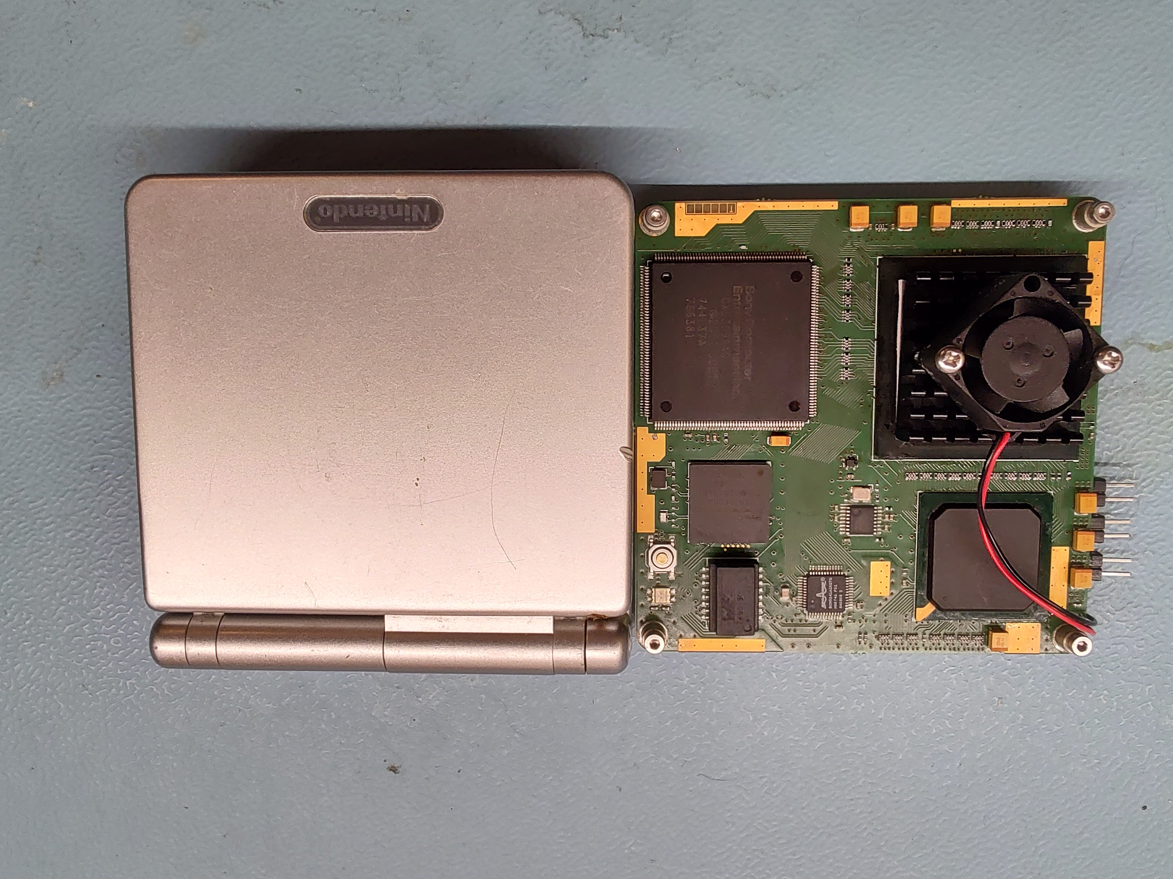
Holy fuck man............ WIZARD!Update time!
3 weeks have passed since my last update and in this time, I went through engineering hell and back.
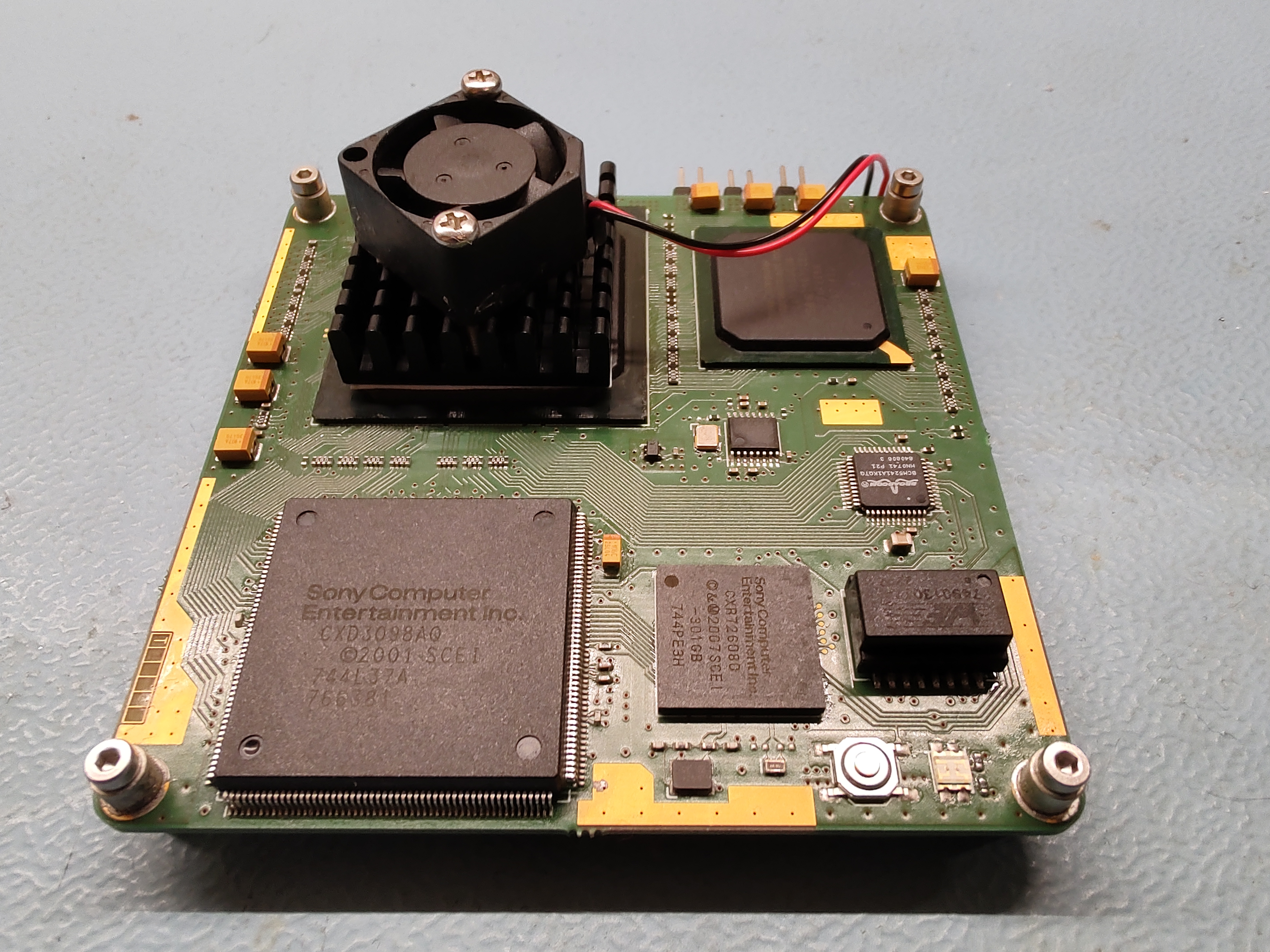
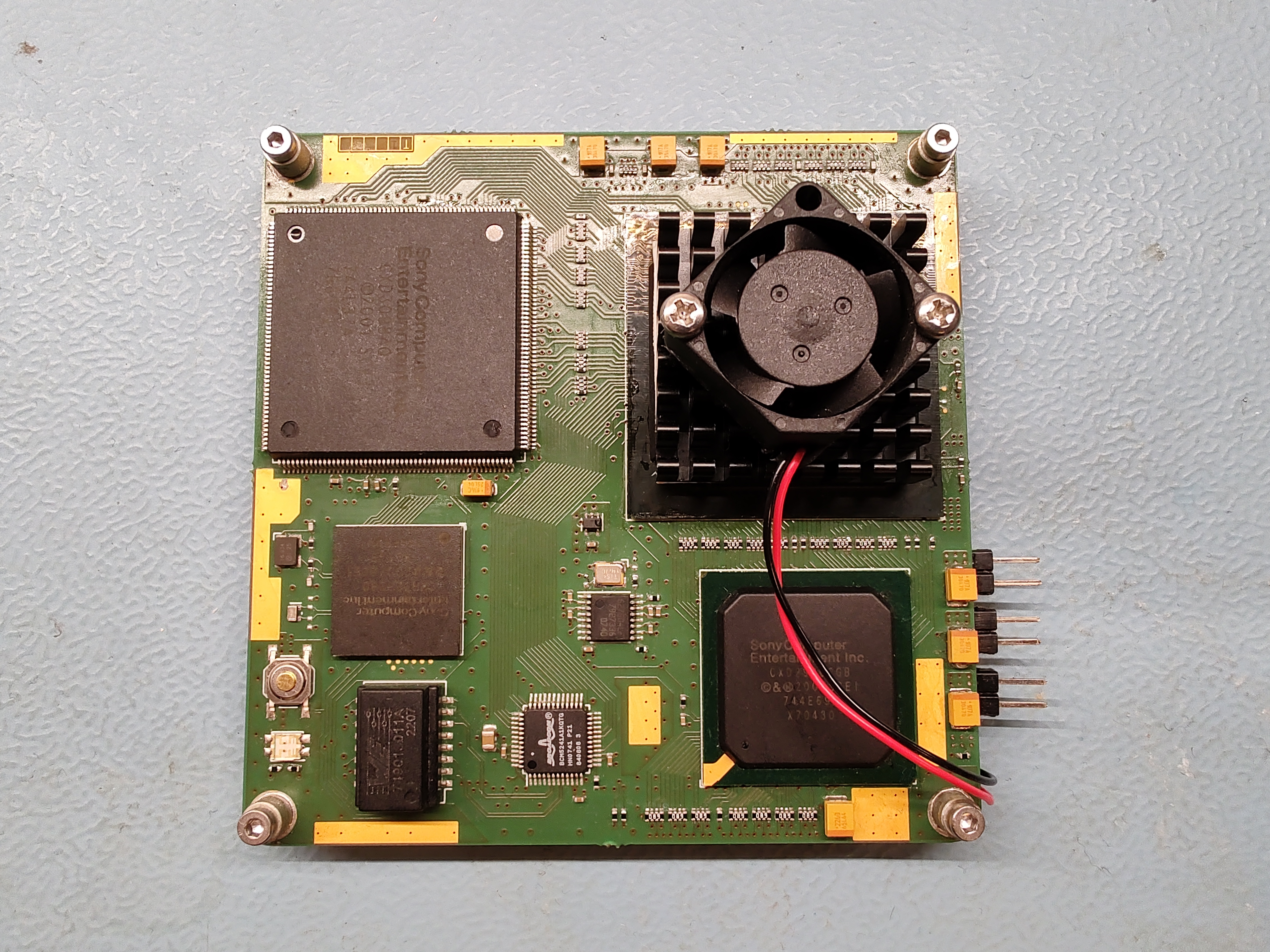
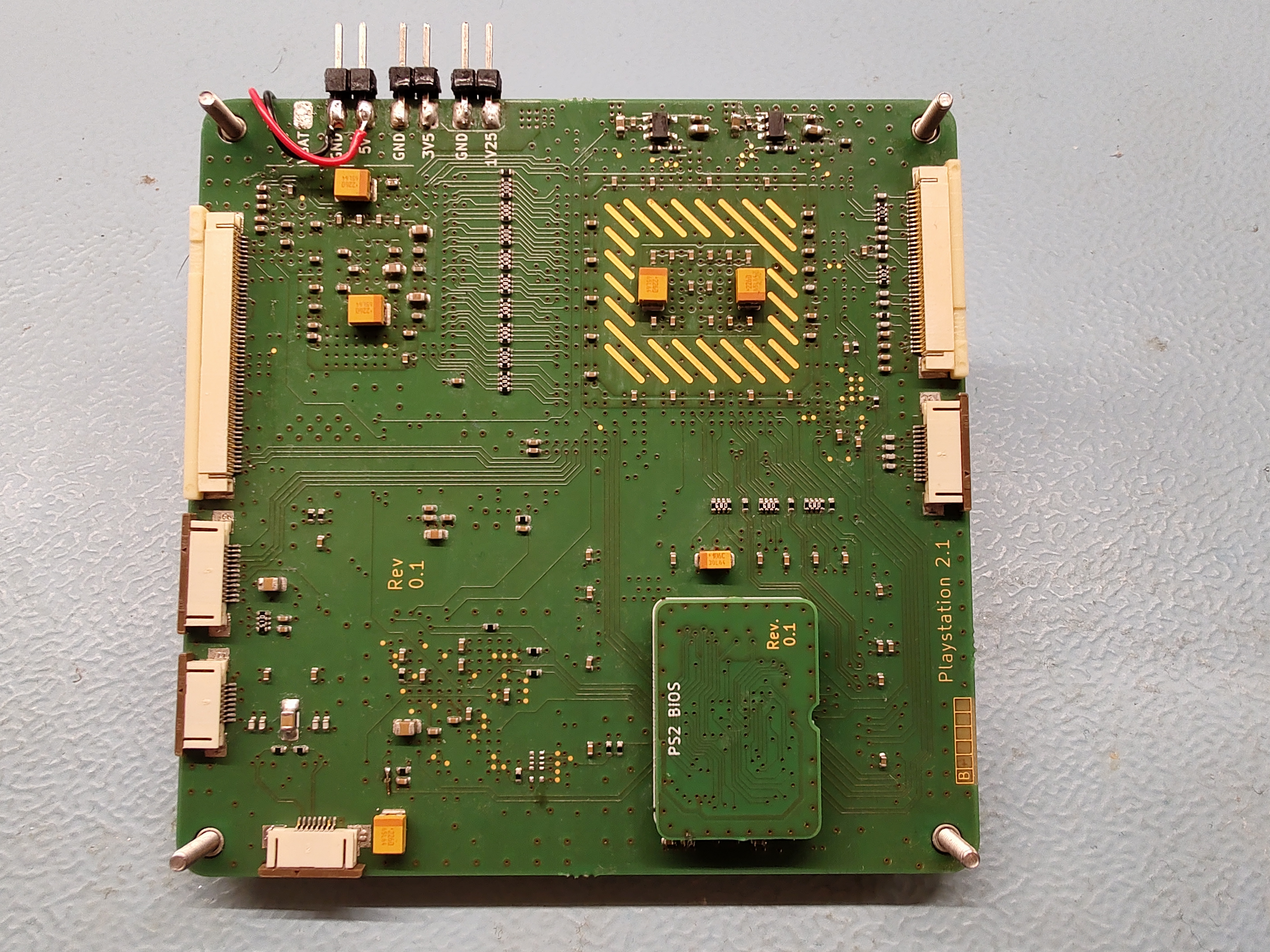
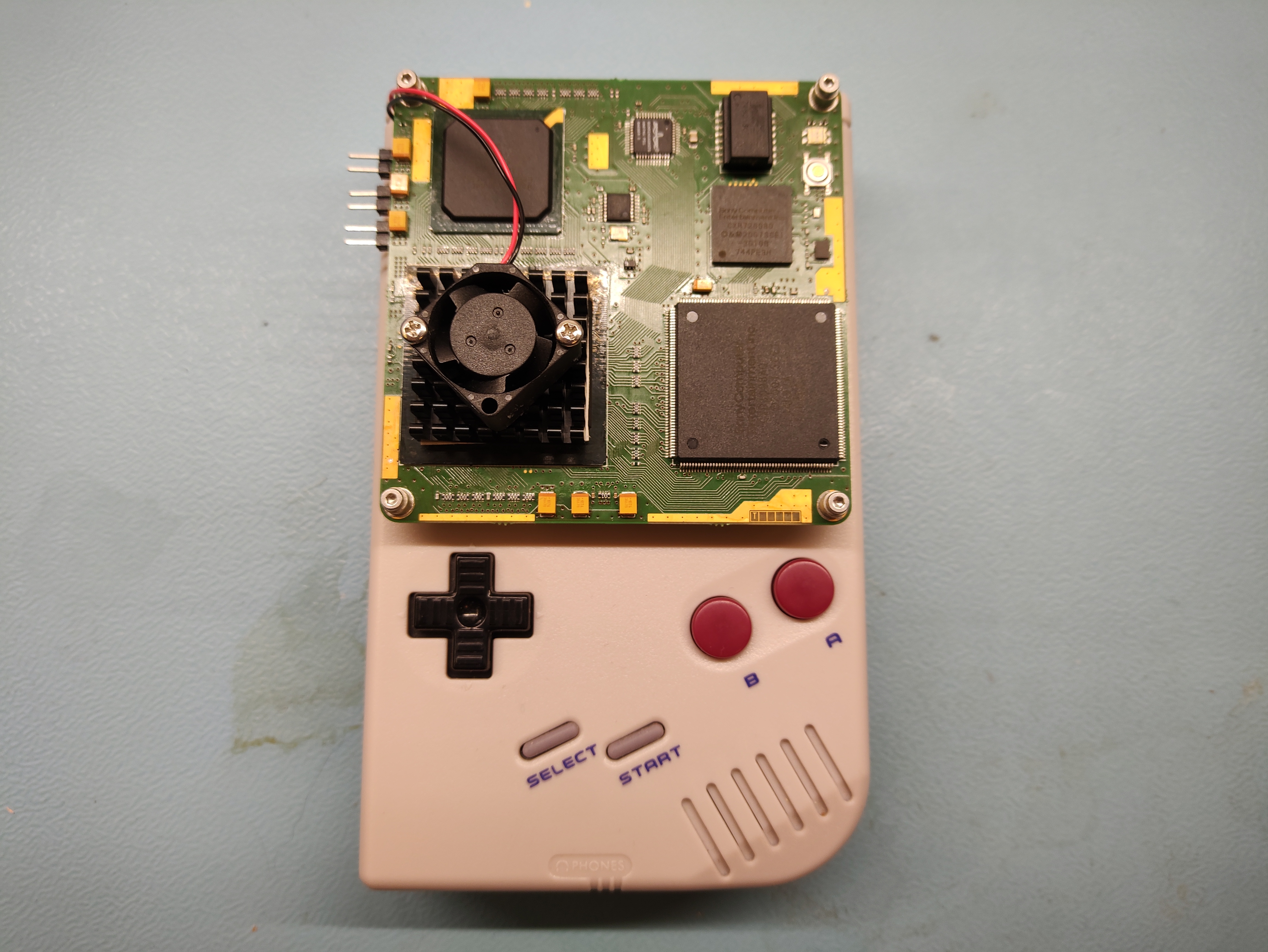
But the hard work was worth it, I am excited to announce that the first prototype of my custom PS2 mainboard finally boots! I literally managed to get it working 2h ago and the system was stable during a quick Okami session. Here it is:
View attachment 26347View attachment 26348
(BTW: my temporary “cooling solution” managed to keep the EE pretty cool, don’t make fun of it! Also please ignore all the flux residue on the board, I call it "battle scars" from 2 weeks of troubleshooting...)
View attachment 26349View attachment 26350
I assembled the board 2 weeks ago with components from my last 79004 mainboard. The reballing process was very smooth, maybe I can give some insight on how the process looked:
Reballing Process
The first step was to desolder the EE, GS, Mechacon, DSP, Ethernet PHY and System clock PLL and to clean them using solder wick. I did the desoldering using my IR preheater and hot air tool, that makes it a lot easier to melt the original lead-free solder. The temperature on the preheater was set to ~360°C and the hot air to 320°C, 90% airflow, that gave pe pretty good results without cooking the chips too much.
View attachment 26351View attachment 26352
I can recommend to clean the pads of the BGAs very thoroughly using solder wick, that way the solder balls stay in place much nicer later on. It is also important to apply as little force as possible on the pads while cleaning. When that was done, I cleaned the flux residue on the 3 BGAs using 99% isopropanol.
With that preparation done, I continued to mask the unused holes in the stencil. I’m using a 0,55mm universal stencil with 1mm pitch. In case anyone has the same reballing fixation, I applied some kapton tape in 2 diagonal corners to prevent the lid from moving around too much, as the sloppy tolerances made the alignment really tricky.
View attachment 26353View attachment 26354
The next step was to apply a thin layer of tacky flux on all pads of the BGA, I used my finger to spread it evenly. The BGA was mounted in the fixation and the stencil was aligned very carefully. The vertical alignment is also VERY important! If the distance between BGA and stencil is too big, the solder balls will not be aligned. If the distance is too small, the balls will not stay inside the holes and when they pop out, they will contaminate the top of the stencil and the other solder balls with flux. That causes the balls to get stuck in the stencil when lifting it off the BGA (which is a big pain, as those balls will have to be placed manually). Always clean the stencil after reballing!
When all balls are in place, I use the preheater and hot air again to melt them. I had good experiences with putting the BGA on an unused stencil and having it over the preheater (set to ~360°C). I usually set the hot air to 320°C, 10% airflow to not blow the balls away while heating. That way, I can slowly hover over all pads until all balls are soldered.
View attachment 26355View attachment 26356
That’s the reballing procedure I followed for the EE, GS and Mechacon. One thing that really annoyed me was the fact that I only have one stencil. That means I have to mask the holes 3 times to reball the 3 chips. Having 3 stencils would save a lot of time, so I ordered new ones from aliexpress.
Placement
Next was the component placement. There is this fancy KiCad plugin called “Interactive HTML BOM” which exports the BOM and a visual guidance where to place the components on the board. Man, I love that thing and I whish Altium had something similar, it makes the component placement SO MUCH easier.
The first side to be populated was the bottom layer. I ordered a solder paste stencil together with the PCBs, so that was very straight forward. When all components on the bottom were placed, I put the board on the preheater again and soldered everything using hot air on a first reflow run.
After that, I put copper tape on the ffc sockets, the mezzanine connectors and the LDOs to prevent them from falling off during the second (top side) reflow.
Then I turned the board around and populated everything on top, except the 3 BGAs. When the top side was done, I put the board back on the preheater at 360°C. I applied a thin layer of flux on all BGA pads of the PCB and placed the BGAs on the PCB. At work, our PCBA assembly house usually does it the other way around – they dip the BGA balls in a low viscosity flux before placing them.
The alignment of the BGAs was very easy, because I have the exact size of the package outlined on the silkscreen – I would highly recommend that for hand-assembly.
Then it was just a matter of heating the board up to solder all components. The BGAs are usually a bit more difficult to observe without the right equipment, so I always give them the -tiniest- push and when they “float” back into position, the connections are good.
After slowly cooling down the CBA, I measured the resistances on all supply rails and they seemed OK.
View attachment 26357View attachment 26358
View attachment 26359
Testing
That was the point where the fun started…
When powering the mainboard on for the first time, the red power LED turned on – so far so good. When pressing the reset button, the LED turned green, but the current consumption stayed at around 200mA. The board was completely dead, there was no video, no audio and not even bus activity on the EE-GS bus and the EE-DSP bus.
I compared most signals to a working board and saw that the EE was not even initializing when powering the board (with the red LED on).
On the good board, even before pushing the reset button, most signals between the EE, GS, DSP were initialized HIGH, the clocks for the EE, GS and ethernet PHY were present. The EE was outputting clocks for the DSP and for the GS. When pressing the reset button the console boots normally with bus activity everywhere.
On my board, a lot of the connections between the EE, GS and DSP were floating at around 0,3-0,6V. The respective clock signals for the EE, GS and ethernet PHY were present, so the system clock PLL was working. The EE did not output clock signals to the GS and the DSP. The CE and OE for the DSP/BIOS were floating at 0,3V, on the good board they were HIGH.
The GS did output a clock to the EE and the Mechacon also seemed to do its job – it tried to boot the system, tried to enable the supply rails and it was outputting a clock to the EE when pressing the reset button. What did not work, though, was turning the system off – it looked like the Mechacon was waiting for something.
These observations made me rule out the GS, clock PLL and Mechacon in my attempt to find the fault. The remaining suspects were the EE (highly sus), DSP and ethernet PHY. What made me rule out the DSP and ethernet PHY in the end was the fact that they were also doing nothing on the working mainboard, at least before pressing the power button. Everything that was supposed to come from the EE was missing on my mainboard and that led me to suspect three likely causes for my issues: wrong connections in my design, bad solder joints on the EE and a broken EE.
I decided to first compare my design to the original mainboard again to find the potential wiring issue. The second and more dangerous step was to replace the EE to solve the remaining 2 issues I suspected. I was a bit hesitant with replacing the EE, as there is a high risk of destroying the board in the process (and wasting a good chip while fixing nothing), so I continued with cross-checking the connectivity of the design. I had my design and the original mainboard next to each other and spent 2 weeks comparing every connection by hand using a multimeter. The conclusion from that was that there is no difference between the 2 boards that would prevent mine from booting. Dead end.
View attachment 26360
That forced me to replace the EE today. As I don’t have any more 79004 mainboards in stock, I had to salvage the new EE from a 90004 mainboard.
Side note: I decided to stop looking for 79004 mainboards, they are just impossible to find. Not a single reasonably priced one was available in the last 6 months and since the PS2 Ultra Slim was released, there are a lot of people actively searching for those mainboards. Importing 79001 consoles is not an option either, as the shipping is usually >50 bucks. Thankfully, nobody wants the 90004 and they are on sale for ~15 bucks quite regularly. I currently have 4 of them in stock and order new ones as soon as they are available.
After replacing the EE, my mainboard finally boots into FMCB. I still don't know whether the issue was a broken EE or bad solder joints, but knowing that I soldered the board at 2AM, I would expect the latter to be the case.
What is currently tested: memory cards, gamepads, loading games from USB. Muting the audio when resetting the console is not working currently, because it's not implemented in my video/audio relocation. You hear it when turning off the console while running a game – there is a loud buzzing sound for 1-2 seconds before the console turns off.
I also noticed something else: the new EE from my spare 90004 mainboard is different from most other EEs I’ve seen. That donor console also had a MUCH smaller cooling solution. During testing, I noticed that this new EE (subjectively) runs cooler that the one found on my reference mainboard. My custom mainboard also draws ~200mA less (currently at ~800mA@8,5V without anything plugged in) than my modified original mainboard.
Speaking of current consumption – I’m very happy with that. With a BlueRetro, a memory card and a USB stick plugged in, the console consumes ~8,9W.
Testing is still ongoing, of course!
View attachment 26361
Front IO Breakout
Here is a closer look on my front IO breakout board. It works great so far. I still have to design a custom fixture for the memory card locking mechanism.
View attachment 26362View attachment 26363
I’m tired and dizzy from all the flux fumes today, so I will end it there (Note to self: buy a proper fume extractor one day). Please excuse any mistakes I made in the update, I'm completely done for now. There will be another update on how I’m planning to continue soon, but this week I will probably take some time off from the PS2 project. I will also have to clean all evidence of 2 weeks of troubleshooting off my lab bench before continuing with anything…
View attachment 26364
N64 and PS2 down, just the Wii left to go! THEY SHALL ALL BE SMALL!
Should rename this thread from "Some PS2 Project" to "*THE* PS2 Project", as that's currently the state of things!
Incredible work, can't wait to see what comes of this. Next thing to look at would be to see how doable mounting the EE on the other side of the board would be. That would significantly shrink the size of the board down. Might need a proper BGA soldering setup for that though :/
Incredible work, can't wait to see what comes of this. Next thing to look at would be to see how doable mounting the EE on the other side of the board would be. That would significantly shrink the size of the board down. Might need a proper BGA soldering setup for that though :/
cfc_12
.
OMG man,
Now, that's an insanity of amazingness!
You're like on a Gman level!
Now, that's an insanity of amazingness!
You're like on a Gman level!
Tschicki
.
Thanks!
I said that I would take this week off, but I couldn't resist...
I've played some games on the board now for a couple of hours and.... man, I hate USB loading; loading times are terribly slow, FMVs are hardly watchable and compatability is trash. And don't get me started on all the fragmentation errors when having more than 3 games on my USB... I think the universe is trying to tell me to finally design an ffc adapter for my smb server! That will make testing easier and more reliable, I hope.
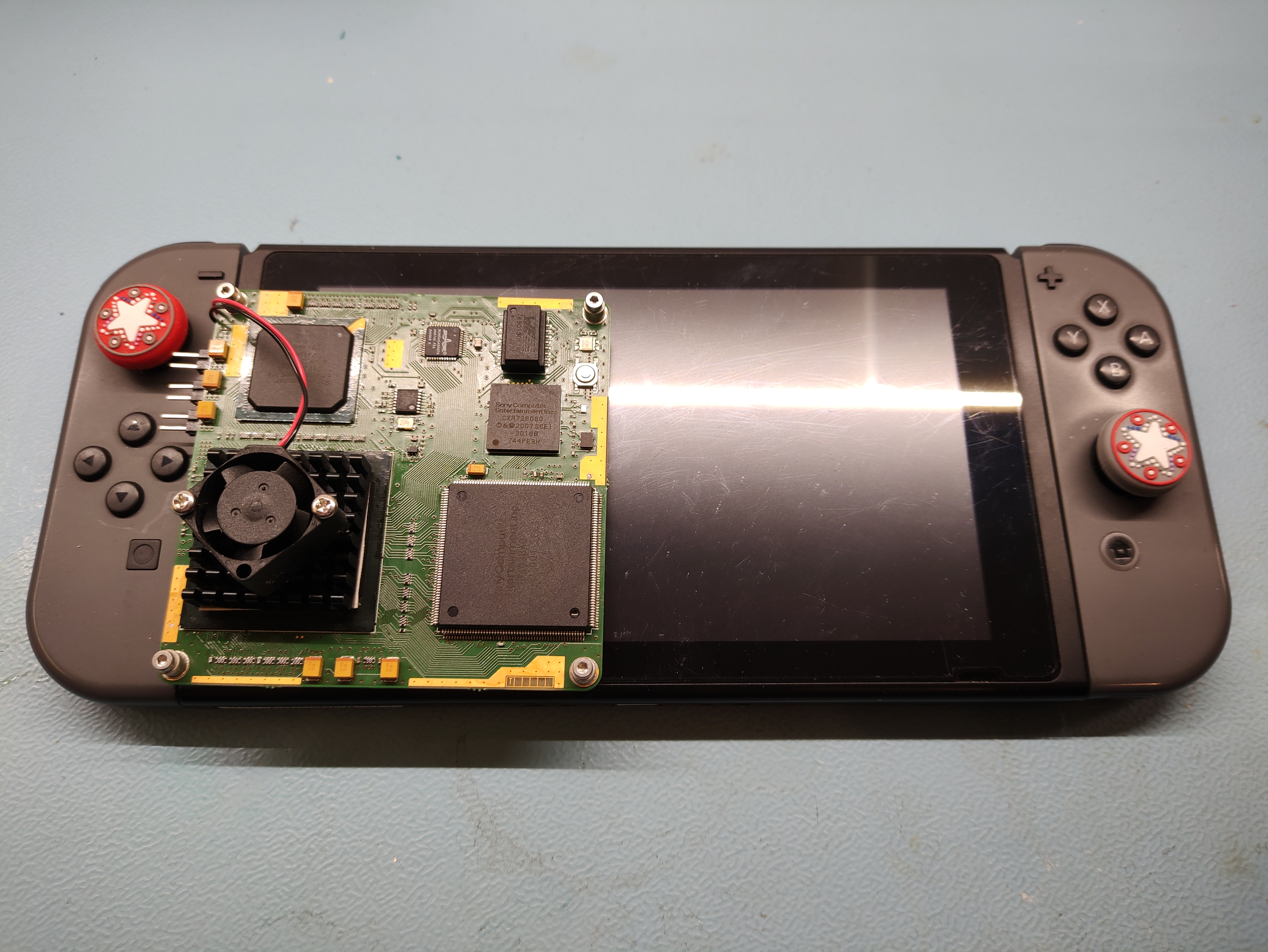
The hardware on the other hand is very stable so far. Apart from incompatibe games, there was not a single crash during gameplay and the longest uninterrupted playing session I had was ~3h(Okami). I also managed to create an improved temporary cooling solution out of parts from my junk bin, a sad looking 20mm fan from another project and a tiny heatsink. It works surprisingly well, keeping the EE hand-warm after 2-3h of playing.
The flux residue was bothering me, so I cleaned it off nicely. Now I can give you some close-ups without feeling ashamed of that filthy prototype.
Now that I have a working design, I took a step back to sort out my priorities. There are still a couple of things to design/test, before I'm fully satisfied with my current testing setup:
The plan for the future is to work on a handheld console (when the mainboard design is ready) and from now on I will keep that system in the back of my head when implementing new things.
The first thing where this applies is the regulator board and I think it makes sense to already design it with a future portable in mind. In order to do that though, I have to know roughly how the system architecture will look like.
That's why I started thinking about the system architecture and power delivery concept of the portable this week. There will be an update on that soonish...
As you all know, engineering is always about finding the most ideal compromise. I'm currently compiling a list of benefits and drawbacks of different cell configurations for the battery. My two options are 1S2P and 2S1P. I know it might not sound like a big deal, but a 1S or a 2S battery will have a big impact on all aspects of the power management design.
I would also be interested in hearing opinions and experiences of other people here! Suggestions would be much appreciated!
I also started to think about possible form factors for the portable. Hmmm....
My favorites so far are the PS Vita (might be tight though) and the Switch, but starting from scratch with a custom form factor sounds exciting too! Will think about it...

I said that I would take this week off, but I couldn't resist...
I've played some games on the board now for a couple of hours and.... man, I hate USB loading; loading times are terribly slow, FMVs are hardly watchable and compatability is trash. And don't get me started on all the fragmentation errors when having more than 3 games on my USB... I think the universe is trying to tell me to finally design an ffc adapter for my smb server! That will make testing easier and more reliable, I hope.
The hardware on the other hand is very stable so far. Apart from incompatibe games, there was not a single crash during gameplay and the longest uninterrupted playing session I had was ~3h(Okami). I also managed to create an improved temporary cooling solution out of parts from my junk bin, a sad looking 20mm fan from another project and a tiny heatsink. It works surprisingly well, keeping the EE hand-warm after 2-3h of playing.
The flux residue was bothering me, so I cleaned it off nicely. Now I can give you some close-ups without feeling ashamed of that filthy prototype.
Now that I have a working design, I took a step back to sort out my priorities. There are still a couple of things to design/test, before I'm fully satisfied with my current testing setup:
- Ethernet (SMB game loading)
- I have to design an adapter to connect my SMB server via ffc
- my BIOS fix by tapping off the DSP CE
- I will need to design a new BIOS module with the S29JL064J55TFI000 and the inverter
- Mister M suggested to try undervolting the EE to reduce the power consumption, I would like to do some feasibility on that.
- My current 1V25 regulator does not go below 1.2V, so my plan is to design a new regulator board (also to get rid of that big chungus of a regulator board)
I'm also thinking about that, maybe that's something to test in an upcoming revision. It will not be possible without moving the GS too, as the pinouts are very much optimized for the current placement. That would mean EE and GS on one side; DSP, Mechacon, Ethernet PHY and clock PLL on the other side. It would also be an option to split the mainboard in 2 modules and stack them, in case flipping the chips would require an HDI design (always thinking about keeping the cost down). The benefit of that would be that it requires no fancy soldering setup.Incredible work, can't wait to see what comes of this. Next thing to look at would be to see how doable mounting the EE on the other side of the board would be. That would significantly shrink the size of the board down. Might need a proper BGA soldering setup for that though :/
The plan for the future is to work on a handheld console (when the mainboard design is ready) and from now on I will keep that system in the back of my head when implementing new things.
The first thing where this applies is the regulator board and I think it makes sense to already design it with a future portable in mind. In order to do that though, I have to know roughly how the system architecture will look like.
That's why I started thinking about the system architecture and power delivery concept of the portable this week. There will be an update on that soonish...
As you all know, engineering is always about finding the most ideal compromise. I'm currently compiling a list of benefits and drawbacks of different cell configurations for the battery. My two options are 1S2P and 2S1P. I know it might not sound like a big deal, but a 1S or a 2S battery will have a big impact on all aspects of the power management design.
I would also be interested in hearing opinions and experiences of other people here! Suggestions would be much appreciated!
I also started to think about possible form factors for the portable. Hmmm....
My favorites so far are the PS Vita (might be tight though) and the Switch, but starting from scratch with a custom form factor sounds exciting too! Will think about it...
Last edited:
Tschicki
.
Small update!
Ethernet
SMB game loading is fully working, no modifications required! I figured it would be easier and faster to solder the ffc adapter for my mini router by hand, it's just 8 wires. Not my finest soldering job, but it will do just fine for testing. Below is an image of the board. The nice thing about it is that the ffc also includes 5V and GND -> all I need to get the router running is really just that 8 pin ffc. That was actually the last feature to test on the mainboard itself.
The games that were tested so far via SMB include Rayman 3, Okami, NFS MW, Shadow of the Colossus, Ratchet&Clank and GTA San Andreas. There was not a single crash so far and especially GTA was running for a couple of hours - time really flies once you spawn a hydra jet...
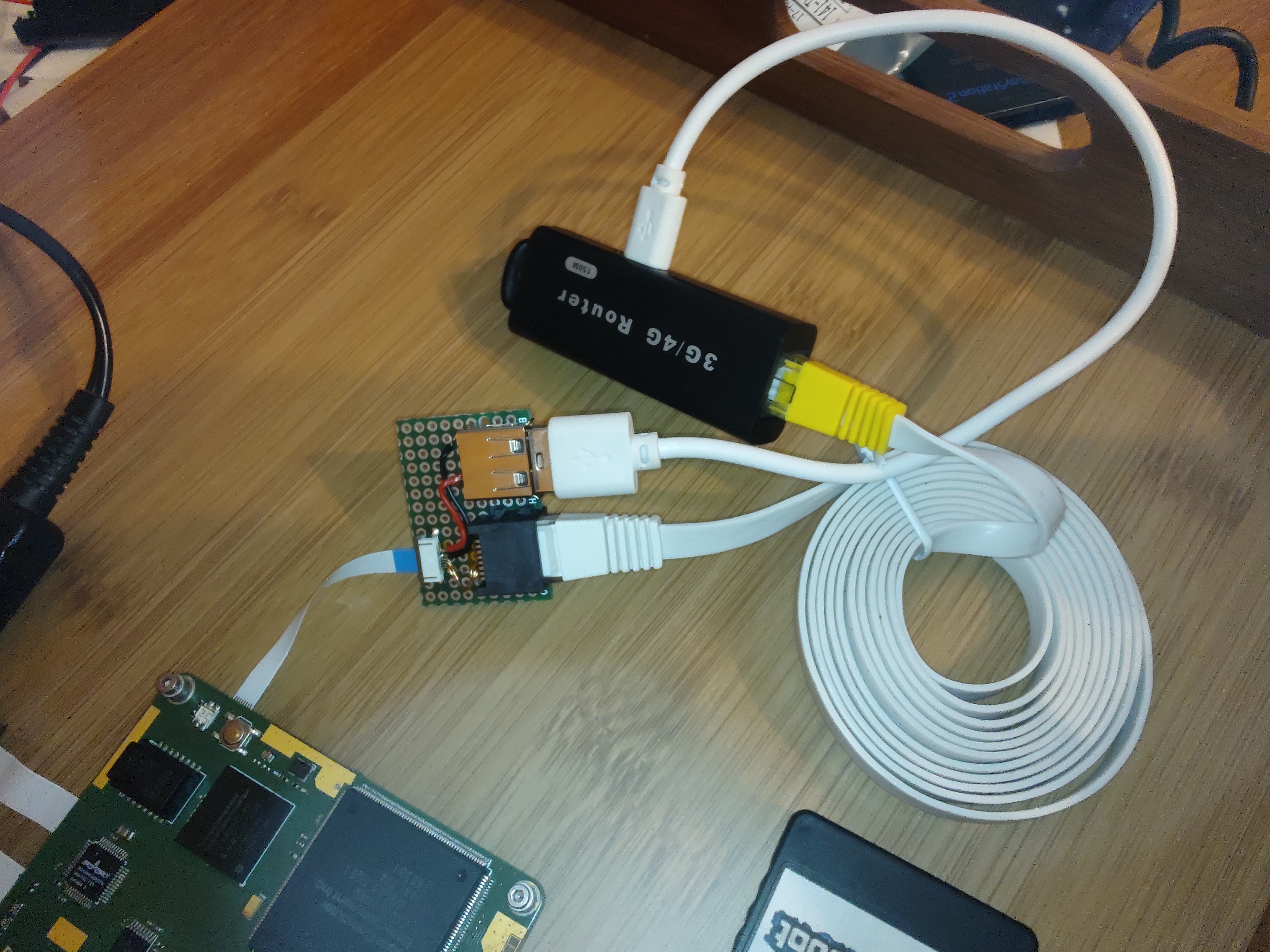
BTW the mini router I'm using is from Aliexpress, just search for "3G mini router". I saw it in one of Mister M's posts and ordered a couple for testing - at 7 bucks per piece. It's not the most reliable router - I ordered 3 and at this point only one still works - but the power consumption is outstanding at ~1W + it is very small.
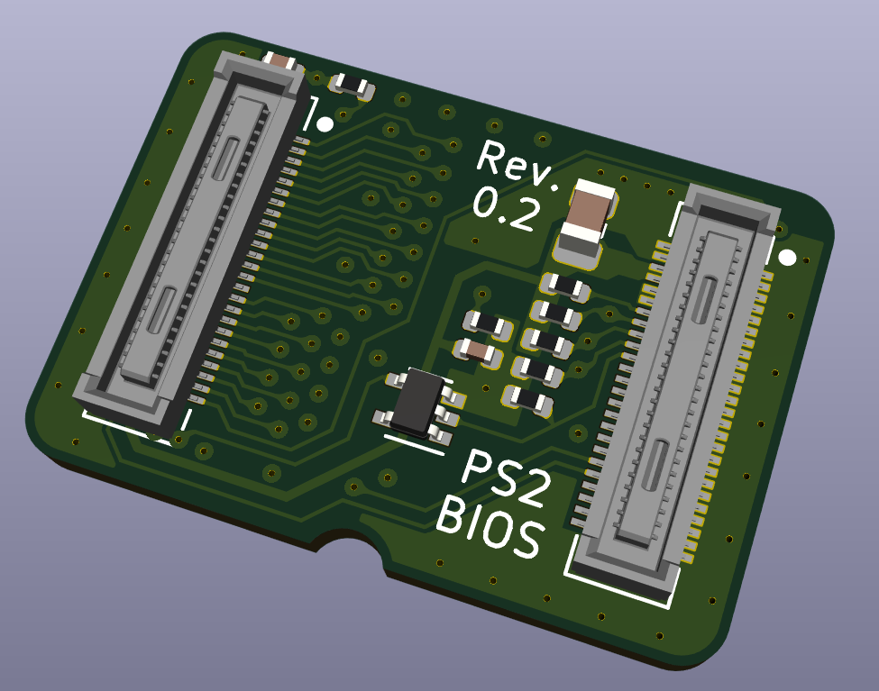
BIOS Module with CE-fix
The module was designed and ordered. The 74LVC1G04 inverter is now included in the module, it will require one bodge wire on the mainboard between /XHCE (DSP pin 169) and the module's CE pin.
Regulator Board
In order to have a rough guideline when designing the regulator board, I came up with a draft power supply concept. It is by far not final, but it should provide good input when searching for ICs and doing the schematics. Ideas for improvements would be very welcome!
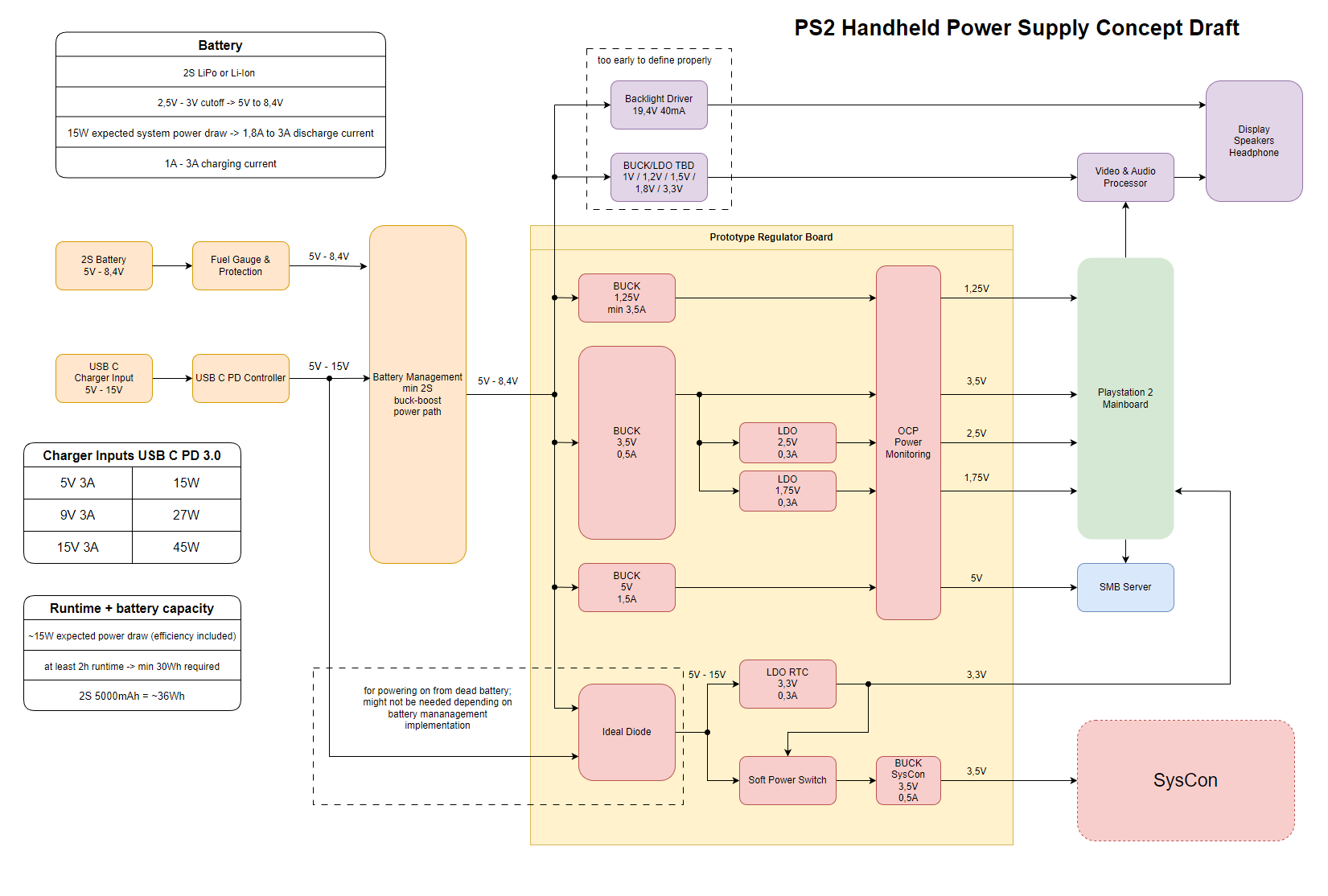
The current plan:
I will work on a prototype of the red blocks in the upcoming weeks. Then I can also test undervolting the EE, as suggested by Mister M.
When that is working, I will move on to the orange blocks (battery management). From time to time I will also work on the purple blocks, as they are a challenge on their own and I expect the implementation to be very time consuming.
I'm doing the design in smaller chunks on purpose, because it will be easier to test and troubleshoot a modular system + it helps to keep me motivated when I can achieve a bunch of smaller successes by getting the subcircuits working. The size of the system is also not one of my concerns right now, miniaturization will start when the circuits work as expected.
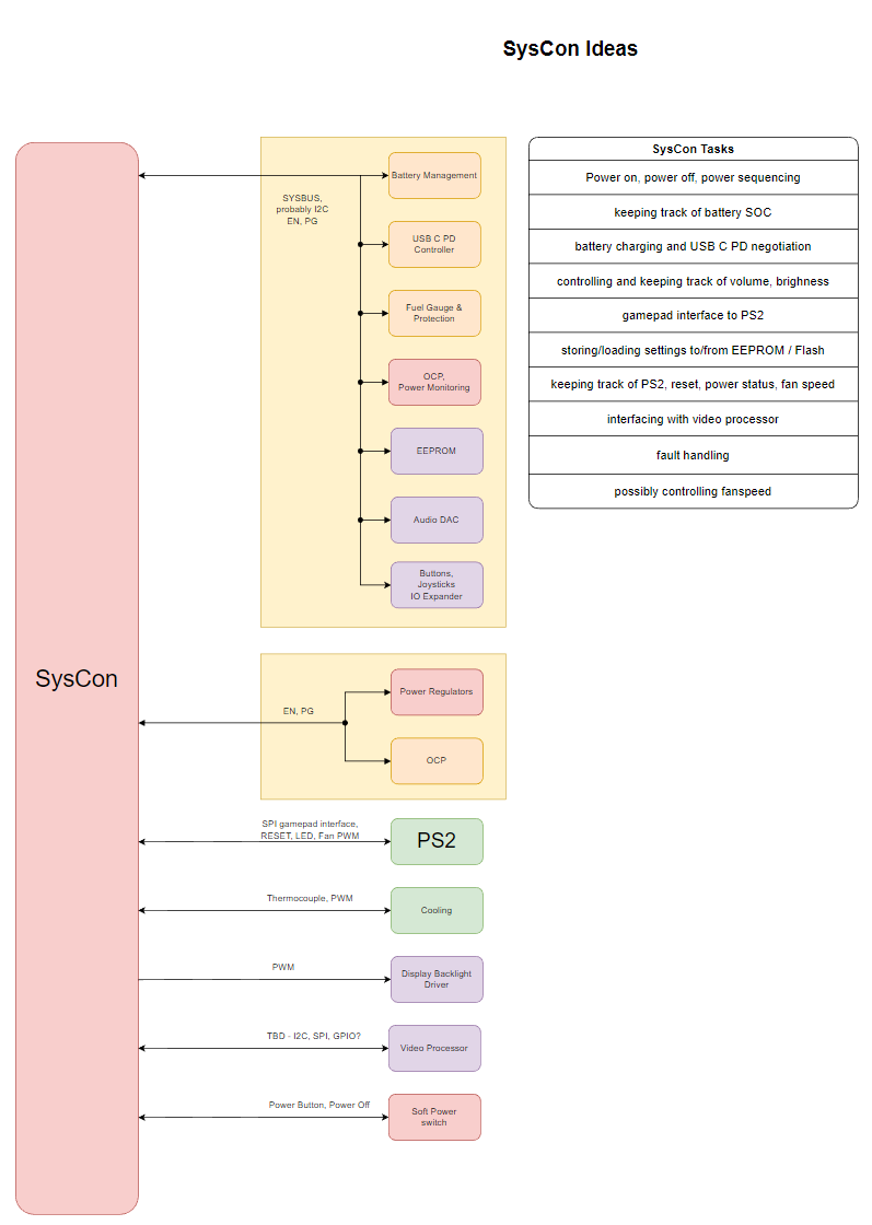
SysCon
While thinking about the power management & architecture, I quickly realized that I will need some sort of system management controller to handle everything except running the games. That includes USB C PD, battery management & SOC, power on & off & sequencing, fault handling, gamepad inputs, audio & video output settings. The preliminary name for it is SysCon, in memory of the PS2 SysCon that was removed after the 39k revision. I've written dowen some tasks and interfaces that I would like the SysCon to handle. There is no decision for a mcu yet, but right now I'm thinking about using a mcu in the STM32L4 series, because I already have some experience with them.
Not all tasks will be implemented right away, the first things will probably be power on & power off + maybe looking into the PS2 gamepad interface.
Ethernet
SMB game loading is fully working, no modifications required! I figured it would be easier and faster to solder the ffc adapter for my mini router by hand, it's just 8 wires. Not my finest soldering job, but it will do just fine for testing. Below is an image of the board. The nice thing about it is that the ffc also includes 5V and GND -> all I need to get the router running is really just that 8 pin ffc. That was actually the last feature to test on the mainboard itself.
The games that were tested so far via SMB include Rayman 3, Okami, NFS MW, Shadow of the Colossus, Ratchet&Clank and GTA San Andreas. There was not a single crash so far and especially GTA was running for a couple of hours - time really flies once you spawn a hydra jet...
BTW the mini router I'm using is from Aliexpress, just search for "3G mini router". I saw it in one of Mister M's posts and ordered a couple for testing - at 7 bucks per piece. It's not the most reliable router - I ordered 3 and at this point only one still works - but the power consumption is outstanding at ~1W + it is very small.
BIOS Module with CE-fix
The module was designed and ordered. The 74LVC1G04 inverter is now included in the module, it will require one bodge wire on the mainboard between /XHCE (DSP pin 169) and the module's CE pin.
Regulator Board
In order to have a rough guideline when designing the regulator board, I came up with a draft power supply concept. It is by far not final, but it should provide good input when searching for ICs and doing the schematics. Ideas for improvements would be very welcome!
The current plan:
I will work on a prototype of the red blocks in the upcoming weeks. Then I can also test undervolting the EE, as suggested by Mister M.
When that is working, I will move on to the orange blocks (battery management). From time to time I will also work on the purple blocks, as they are a challenge on their own and I expect the implementation to be very time consuming.
I'm doing the design in smaller chunks on purpose, because it will be easier to test and troubleshoot a modular system + it helps to keep me motivated when I can achieve a bunch of smaller successes by getting the subcircuits working. The size of the system is also not one of my concerns right now, miniaturization will start when the circuits work as expected.
SysCon
While thinking about the power management & architecture, I quickly realized that I will need some sort of system management controller to handle everything except running the games. That includes USB C PD, battery management & SOC, power on & off & sequencing, fault handling, gamepad inputs, audio & video output settings. The preliminary name for it is SysCon, in memory of the PS2 SysCon that was removed after the 39k revision. I've written dowen some tasks and interfaces that I would like the SysCon to handle. There is no decision for a mcu yet, but right now I'm thinking about using a mcu in the STM32L4 series, because I already have some experience with them.
Not all tasks will be implemented right away, the first things will probably be power on & power off + maybe looking into the PS2 gamepad interface.
thedrew
.
- Joined
- Sep 27, 2016
- Messages
- 414
- Likes
- 895
looking good! Really love this worklog.
If I can offer a suggestion, I would take a look at MX4SIO instead of SMB loading. Not sure if it works with 9K PS2 models, but don't see why it wouldn't. It will save you space and power since you can run the games off a Micro SD card wired directly to the memory card 2 port. I have tested 30+ games without issue with only 1 game having FMV stutters, which I believe was actually just an OPL compatibility problem. Those games gave me stutters with USB loading but not with MX4SIO. The loading speeds are faster than the slow usb speed. Wesk made a post about getting it working here if you are interested:
https://bitbuilt.net/forums/index.p...-ps2-portable-for-sd-loading-79k-models.4977/
Tschicki
.
That's a good point, thanks! The MX4SIO was completely off my radar for game compatibility reasons, but it looks like they improved it recently!looking good! Really love this worklog.
If I can offer a suggestion, I would take a look at MX4SIO instead of SMB loading. Not sure if it works with 9K PS2 models, but don't see why it wouldn't. It will save you space and power since you can run the games off a Micro SD card wired directly to the memory card 2 port. I have tested 30+ games without issue with only 1 game having FMV stutters, which I believe was actually just an OPL compatibility problem. Those games gave me stutters with USB loading but not with MX4SIO. The loading speeds are faster than the slow usb speed. Wesk made a post about getting it working here if you are interested:
https://bitbuilt.net/forums/index.p...-ps2-portable-for-sd-loading-79k-models.4977/
I ordered the MX4SIO + a samsung SD card and will try to do some tests on the weekend.
There is only one concern I have when it comes to implementing it in my portable. I have a strict requirement for having a full size memory card slot for savegames, because I want an easy way to transfer saves between my fat 39k and the portable. Just to replicate a portion of that retro feeling when you bring your memory card to a friend's place to finish a really hard level on a game.
I'm a real noob when it comes to the software side on the PS2, but as far as I understand, the MX4SIO must be plugged into port 2 and the FMCB card into port 1 of the console. Games are then saved to a VMC on the FMCB memory card? Can you then plug that FMCB memory card into a FHDB softmodded console to continue playing? Maybe I should do some testing on that, because the savegame topic is really important to me.
In case it doesn't work I could think about some ways to develop around this:
- I noticed that unplugging the FMCB memory card is fine after launching a game. Maybe it would be possible to switch from FMCB to a regular memory card for saving games using some logic (e.g. small bus switch) to drive the CE of both cards accordingly. I would just have to figure out how to detect when the PS2 is launching a game.
- Looking into the Multitap would be an option, but I don't really like that idea as it sounds like a lot of additional work for little benefit
- It might sound stupid, but maybe it would be possible to replace the original OSDSYS in the BIOS with the hacked version from FMCB. Or modify the stock ELF loader to load OPL directly from MC or USB during booting. Then I could get rid of the FMCB memory card altogether. In the end I have a reprogrammable BIOS chip, I could flash on there whatever I want. I'm far from knowledgeable enough to pull that off though, but maybe someone on ps2-home/psx-place knows whether or not it would be feasible.
thedrew
.
- Joined
- Sep 27, 2016
- Messages
- 414
- Likes
- 895
Yeah software is not my thing either...but I totally understand the nostalgic factor involved with the memory card. I don't use VMC with MX4SIO to be honest, I save them to the FreeMcboot card in slot one. I would imagine you can still pop in that memory card to another PS2 and load saves just fine but I haven't tested that personally. We are always looking for ways to save space since portables are limited for space, so just thought this would be a great option for your awesome project!
- Joined
- Mar 3, 2016
- Messages
- 2,229
- Likes
- 2,952
- Portables
- 2
Dude, that was an April's fool video lolI have two stuffs you will implement.
Search:
EEVblog 1384 - Halve Your Processor Power Consumption!
I don't think it would halve the power, but i think a 20+% reduction is pretty plausible in this old hardware, this was implemented in the PS3 generation directly on the chip, it would be VERY interesting to see what power reduction is possible on the PS2.
ALSO, forget your ethernet adaptor, you're searching for VOCORE, it runs OPENWRT, has ETH, SD, USB and WIFI and a few GPIOS to have some fun, can't beat it.
Tschicki
.
I appreciate the suggestion, the VoCore2 looks pretty cool actually. I've seen that people were able to get samba working on the Mediatek MT7628 (real shame that you can only get it on aliexpress), so it might be feasible to use it on a PS2. However, I have decided to ditch the SMB game loading entirely and focus on the MX4SIO after running a couple of tests.ALSO, forget your ethernet adaptor, you're searching for VOCORE, it runs OPENWRT, has ETH, SD, USB and WIFI and a few GPIOS to have some fun, can't beat it.
Now that I'm already typing a reply, I can also just give an update.
MX4SIO
As I mentioned already, I will be switching to the MX4SIO for running games on my portable. I got myself a clone MX4SIO memory card and a 128GB samsung SD card and tested ~25 of my favorite games on my prototype. And I have to say that I'm very impressed with the performance when using the latest OPL beta, there were only 3 games that did not work at all. Loading speed is noticably slower than SMB loading, I noticed it especially in GTA SA, where the terrain loading couldn't keep up with the hydra jet quite frequently. When comparing it to the disc version of the game the performance is about the same, so I guess I'm just spoiled by HDD/SMB loading. You could call the MX4SIO more "realistic".
I also tested the same games with SMB loading on my prototype and HDD loading on my 39k PS2 to get a reference for the compatibility. SMB was running all the games just fine and on the HDD only 2 games were broken.
Another important thing for me was that transferring savegames should be as easy as plugging the FMCB memory card into another console. When I have a portable in the future, I want to continue playing the savegames on my TV using my softmodded 39k PS2 without much hassle.
I gave it a try and I can report that it kinda works. The 39k was always booting from the memory card instead of the hard drive in the beginning, but after changing some settings in the FMCB configurator it now boots into FHDB by default. The issue now is that for some reason the 39k takes ages to boot into FHDB when the FMCB memory card is plugged.
The next problem to overcome was OPL. The OPL settings are saved to the FMCB memory card on my prototype and to the HDD on my 39k. Now when I start OPL on my 39k and the memory card is plugged, it always reads the settings from the memory card. That broke OPL, because I was using different OPL versions on the two consoles. I kind of solved it by using the same OPL version and let them share the same settings, but that is still not a perfect solution. Now the artworks are still kind of broken and I guess the compatibility mode settings might be broken too.
I guess I can live with that. It really only is a problem on PS2 fat consoles with FHDB, if I get a slim PS2 with SMB server there should be zero issues.
So the conclusion for myself:
- Is the MX4SIO better than SMB loading?
- No. There are quite some compromises to make.
- Is the performance good enough to justify switching to the MX4SIO in my portable?
- Yes. Considering that the MX4SIO development is relatively new, I see lots of improvements in upcoming OPL versions. It also saves quite a bit of space and the power savings of ~1W should also be considered. There is also less complexity and fewer components that could break.Transferring savegames is a bit of a pain right now, but I'm sure I can find a better solution in the future. At this point I'm totally convinced that the MX4SIO is the best solution for playing games on a portable PS2.
BIOS Module with CE fix
Two modules were assembled & tested and they work perfectly fine. One module has the S29JL064J55 and the other one has the S29JL032J60 to try both speed options. Both of them work and that leaves me with 3 working NOR flash chips to use in my system. Let's also use the time and celebrate the first bodge wire on my prototype! yay!
This was also the last puzzle piece to get the functionality I want out of my reverse engineered mainboard. Now I'm happy with all features and everything is tested and working at this point.
Power Management
There was significant progress on the design of a first prototype. I decided to split the design into 2 boards for flexibility, a regulator board and a base board. The regulator board has all the power regulators for the PS2 and plugs into the base board. The base board includes the SysCon and probably some means to measure the power input/output. The base board is not ready yet, so let's focus on the regulator board:
Following my rough power supply concept I was searching for suitable buck converter ICs to satisfy my requirements.
There were 2 possible directions to take in the beginning:
- an all-in-one power management IC with multiple outputs, like the ADP5052
- discrete regulators for the rails
I did quite some calculations and comparisons, but what ultimately made me go for tha latter approach was flexibility. If I'm not happy with the performance of one rail of the integrated solution, I can ditch the whole chip and I have nothing left. When I have discrete buck converters, I can tailor the features perfectly to my needs (at the cost of added complexity and BOM count, of course)
In an effort to find a good compromise between size, efficiency, cost and my requirements, I have selected the following chips for the first board:
- MPQ8626GD for the 1,25V rail
- TPS629210 for the 3V5, 5V (100% duty cycle operation) and SysCon power rail. Reusing the same chip reduces the BOM count
- ADP123AUJZ for the 2V5 and 1V75 rails
- TPS70933DBVR for the standby regulator (RTC + power switch, low Iq)
The regulator board features a BAT and CHARGE input, in case I need it. There is a charge_detect signal that is triggered by applying a voltage to the CHARGE input. It bypasses the power switch and turns the SysCon on automatically when a charger is plugged. I will need that for handling the charging process and for displaying the SOC. The 1V25 regulator currently has a trimpot in the feedback divider on the bottom layer, that will make undervolting the EE easier. The pins are arranged with a 100mil pitch for using the board on prototyping PCBs. I would like to keep the Iq of the whole system in off state below a couple 100uA, that was also an important consideration when choosing the buck regulators.
The PCB design is 90% finished and the regulators require about 24mmx22mm of space. The layout is still a bit messy for my taste, but optimizing it more for a first prototype would be a waste of time. My plan is to order the PCBs and the components in the upcoming days.
SysCon
The uC for the SysCon was also selected. I will be using the SM32L476, mainly because I found some in my junk box. It's low power, has lots of memory and should be plenty fast for my application. I'm currently working on the pinout of the SysCon and the schematics of the base board for the power management.
The base board might already include some peripherals of the SysCon to play around with.
Soft Power Switch
A quick&dirty prototype of the soft power switch was designed and ordered and I really hope that it works. I'm not a huge fan of the MOSFET based circuits floating around on the internet, so I came up with a circuit based on the 74LVC1G74 D flip-flop. The fact that I have a standby 3.3V rail makes this much easier.
This is how I expect it to behave:
The switch would feature a long press to turn on + long press to turn off - adjustable via R102 and C101. The 74LVC1G74 is edge triggered and has schmitt trigger action on the clock input, so the slow rise time of the power button input should not affect it. The idea of D101 in the circuit is to discharge the capacitor immediately via R101 when the power button is not pressed, otherwise the circuit would be locked for a couple of seconds after each button press. The latch should be reset to a defined (off) state by C104 when applying power, because /RD needs longer to settle. The SysCon has the possibility to force the system on and off via the asynchronous set and reset inputs, overwriting the power button. SYS_VCC_EN feeds into the EN pin of the buck converter powering the SysCon, it can only be bypassed via the charge_detect signal. Powering on and off the rest of the system will then be taken care of by the SysCon. The quiescent current should be pretty low in the uA range.
I don't know whether the circuit really works because I couldn't simulate it (my multisim license expired), but in my mind it should work in this configuration.

We will find out more when I get the power switch assembled!
Last edited:
- Joined
- Apr 5, 2023
- Messages
- 14
- Likes
- 13
If CE1 and CE2 are used, and you need one output, why not use 74hc32 for merging?
Tschicki
.
There are actually no plans to sell any boards. My time for all the hobby stuff is pretty limited and selling things would just take that time away from the things I enjoy doing. Sorry! But I will release the schematics, board layout and BOM for anyone to modify and reproduce, so when the time comes you will be able to recreate a board yourself. Just trying to find the right time to do the release.I am really enthusiastic about your project, when you finish it, will you make your PCBs to order? I would be delighted to buy one from you. Regards
Good point! It would be really interesting to try this!If CE1 and CE2 are used, and you need one output, why not use 74hc32 for merging?
I still have my reference mainboard for BIOS testing and if I find some time, I will definitely try it. Might also be intersting to try a NOR gate too, because in the 70k service manual I just noticed that the CE1 and CE2 inputs are not inverted on one of the OTP ROMS. Maybe I can find the old logic analyzer recording and look into it at some point.
It will have to wait a little bit, because currently my focus is on running the system from batteries + the CE fix is very stable so far.
There will be another update in a couple of days! I just have to do some more measurements before there is something to report.
I'm playing some games using the new regulators right now, here is a small spoiler for the next update:
- Joined
- Apr 5, 2023
- Messages
- 14
- Likes
- 13
I suspect a mistake in my previous post. ROM mx23l6400 consists of two parallel parts. /CS2 enables the first ROM.
- Joined
- Apr 5, 2023
- Messages
- 14
- Likes
- 13
You can try to get rid of the CXD3098Q and CXR726080. First you need to try after initialization to disable the /CS_3098 signal from the CXD3098Q and pull up from the CXR726080. After check the launch of the games.

Tschicki
.
Update time!
I will leave those implementations to the smart people out there, once the design is released. I’m sure there are lots of things to be optimized still!
Now let’s get to the update:
Soft Power Switch
I have a prototype of the soft power switch in a “working” state… kind of.
This is what happened during testing:
When pressing the button for a couple of seconds, the EN went H as expected. But every time I released the button, EN switched off immediately. At that point it was a latching power switch that didn’t latch, just to give a short summary on the functionality.
I suspected some oscillation and hooked up the scope… and there was oscillation. The latch would always oscillate around HIGH threshold, which indicates a lack of hysteresis on the CLK input. This would happen when pressing the button and when releasing the button. That’s why the EN always turned off again.
I “fixed” this by adding a timeout using R103 and C103. This does not prevent the oscillations, but it delays the next state to restore the latching functionality. It works pretty well, but keeping the button pressed for longer than the timeout period breaks the functionality again. That’s because the flip flop already stores the next state during the oscillations when the button is released.
I wasn’t satisfied by this fix and the only way to get the circuit working reliably is to add hysteresis.
That’s exactly what I did: I added a MIC841H voltage comparator between C101 and the CLK input of the latch. It provides adjustable hysteresis using a voltage divider and the circuit works pretty well so far. The only downside is the increased component count. I’m especially unhappy with the added voltage divider for the hysteresis. A Schmitt Trigger buffer like the SN74LVC1G17 would be a more elegant solution, but it has a higher Iq than the MIC841. The Iq is currently at about 3uA.
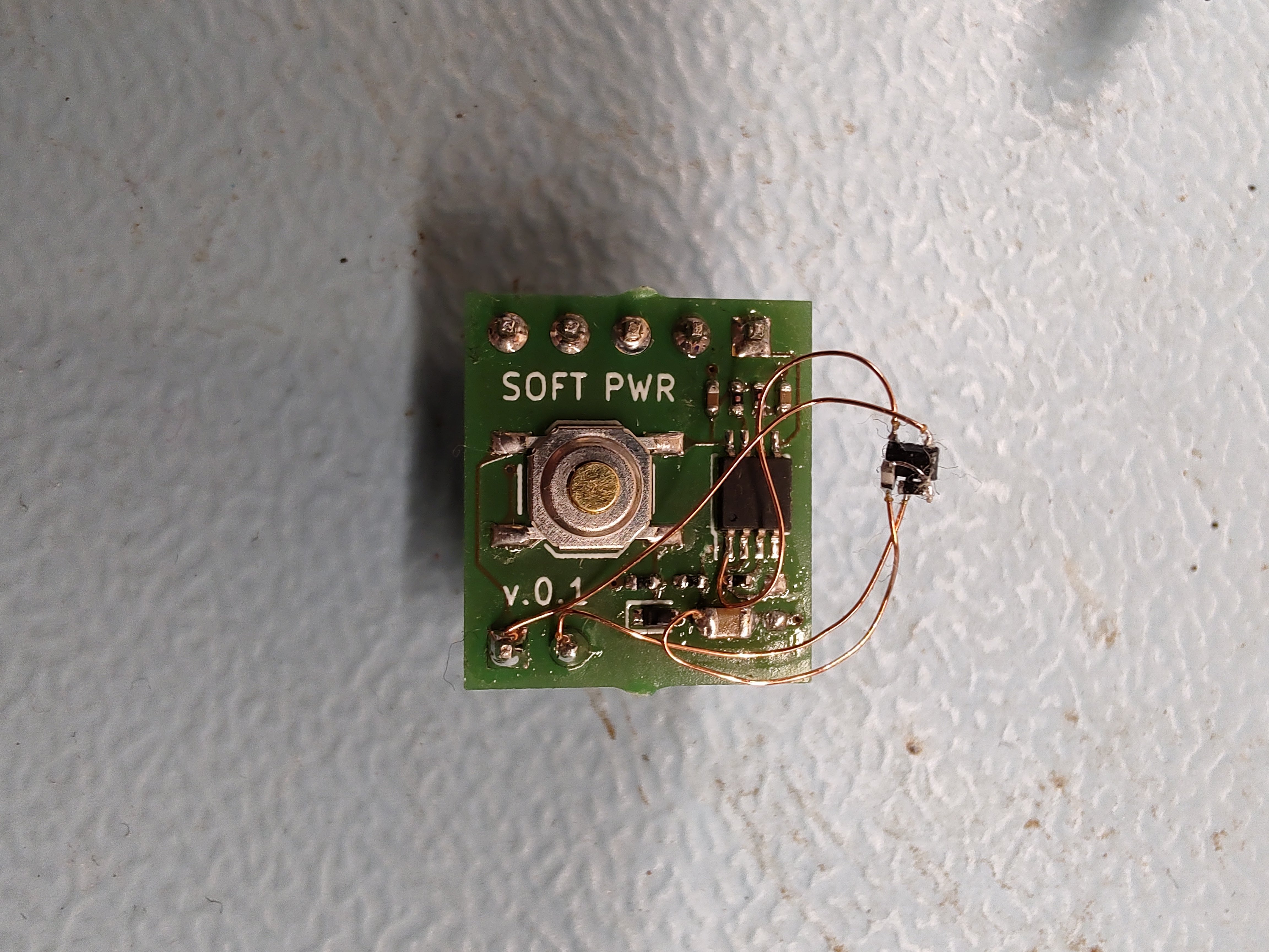
I will try the Schmitt Trigger buffer next, but for now the circuit works as expected: press the button for a couple of seconds to turn on; press it for a couple of seconds to turn off; force the latch on using SET; force the latch off using RESET. The latch also always starts in the OFF position, which is good.
Regulator Board
Now this is an exciting topic to discuss!
I managed to assemble one prototype of the regulator board and did a couple of tests already.
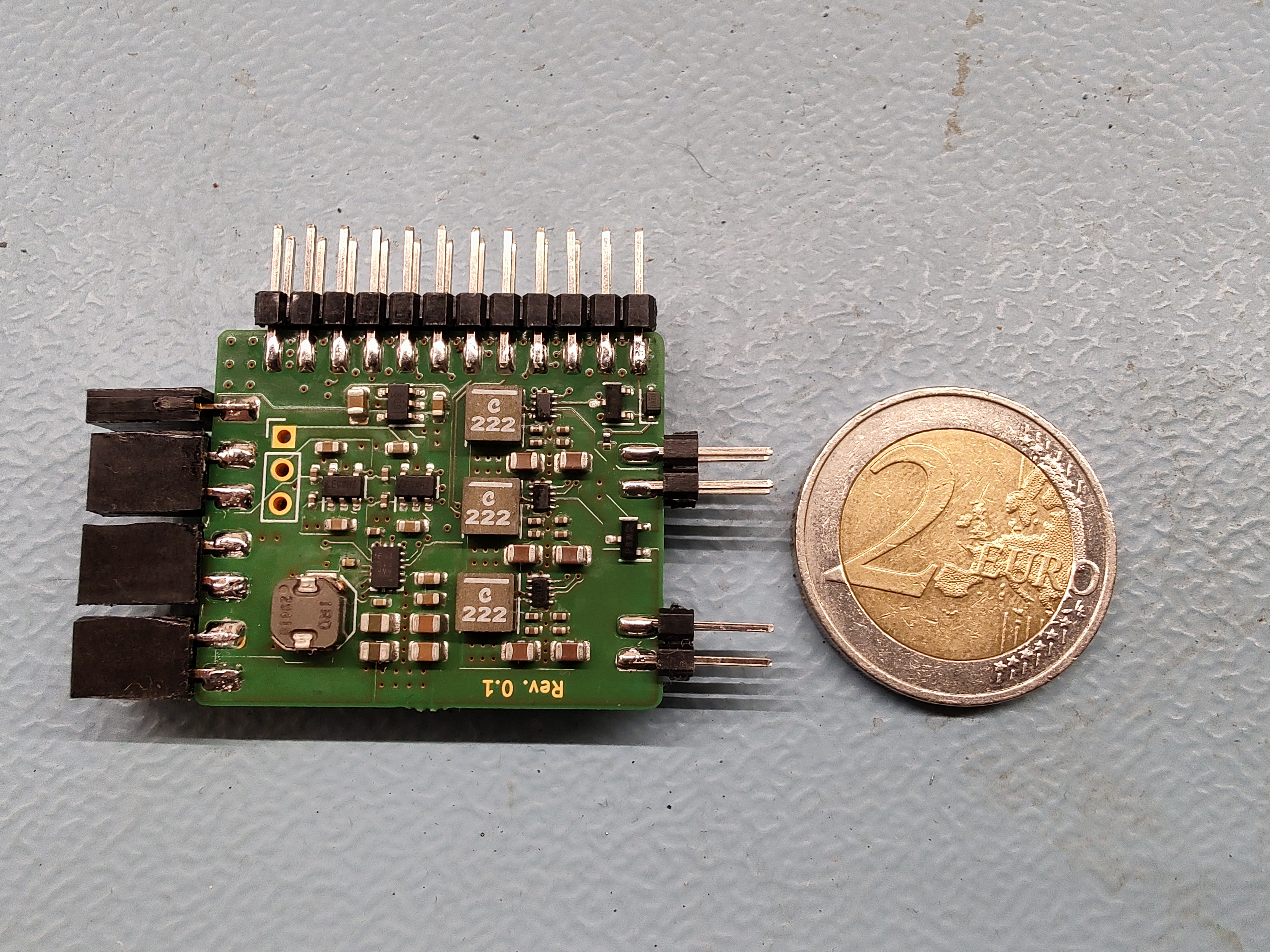
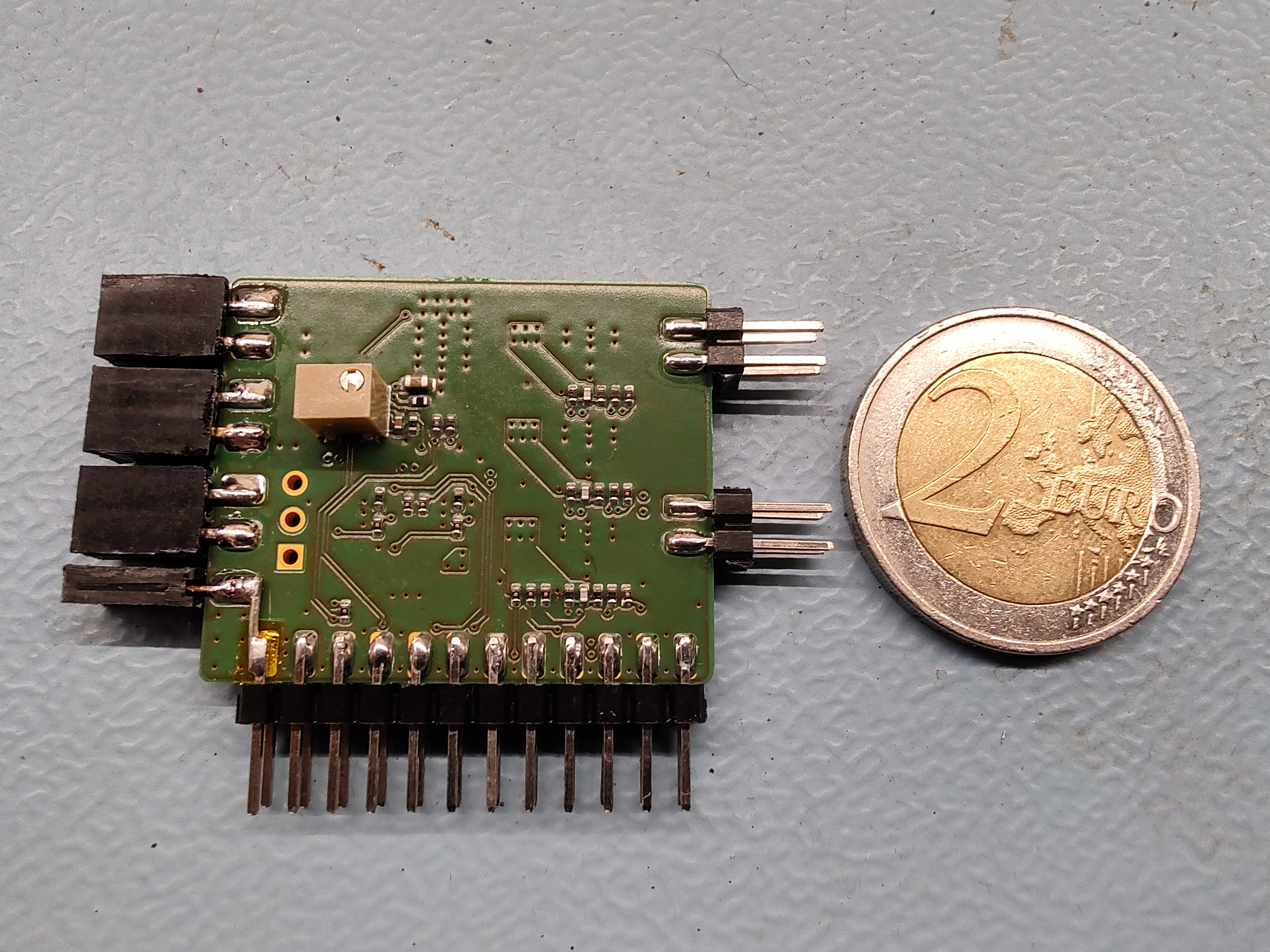
You can spot some differences compared to the picture I shared last time. I decided to arrange the connectors horizontally to make measuring easier, the circuit is identical otherwise. The pin headers make the board look really big, but the bare circuit actually fits within the area of a 2€ coin (25.7mm diameter). The board now contains the buck converters for the 1.25V, 3.5V, 5V, VSYS rails and the LDOs for the 1.75V, 2.5V and standby rails. 7 voltage rails in total, not bad for the size!

You can also see that the soft power switch is already connected to the EN pins of the regulators, this was necessary because I don’t have the SysCon yet and needed a debounced EN signal for the regulators. While connecting everything I realized that stupid me forgot to connect the standby 3.3V rail to the SysCon header for powering the soft power switch. I had to disconnect a pin and connect 3.3V instead (that’s the bodge in the corner).
The other stuff I did is not as exciting, I guess. Let’s get to the tests!
Before connecting the regulator board to my mainboard, I had to verify that it meets my specifications. In the following section I will provide the testing outcomes for information and future reference.
First thing was to find out the input voltage span. The max input voltage is well defined at 8,4V, because I’m planning to use a 2S battery configuration. The min input voltage is mainly defined by the dropout voltage of the 5V buck converter. During testing I found that the 5V regulator is able to sustain the full output voltage at 5.3V-5.4V input voltage (at full load). To give myself some safety margin I set the min to 5.5V, which means that I would be able to discharge the batteries to 2.75V (if needed).
That means the preliminary input voltage span is 5.5V to 8.4V and it's what I used as the base for further testing.
(Boring stuff starts here)
Let’s start with the efficiency and load regulation plots:
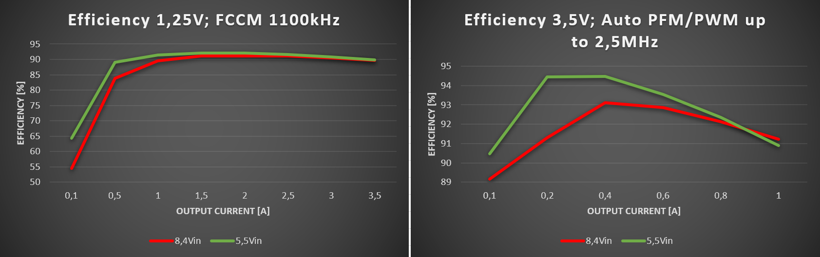
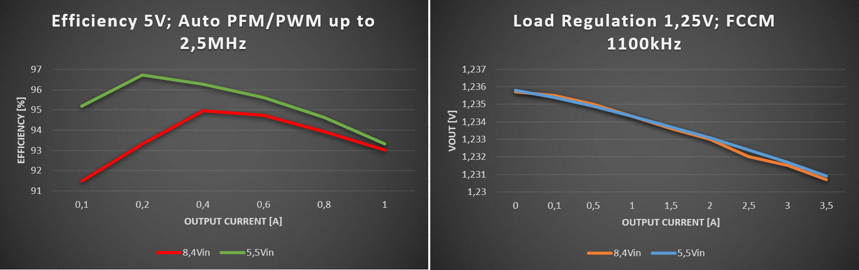
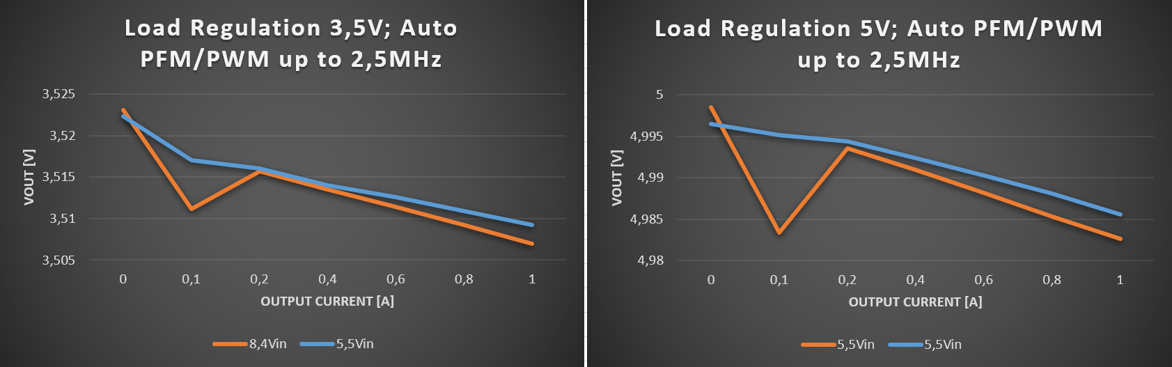
The plots above are lacking a few data points (I was too lazy to do more measurements), but they provide plenty information for my evaluation. The first thing that catches my eye is the bad efficiency of the 1.25V converter below 1A. This is expected, because I forced the converter into continuous conduction mode, which gives lower efficiency with light loads. That saves me another resistor value in the BOM and it doesn’t matter, as the converter is fully loaded 99% of the time.
You can see the difference in light load performance when looking at the 3.5V and 5V rails. They are configured to enter power save mode on light loads. The 5V rail will only be loaded when a USB stick is plugged (in the next revision; currently supplies the USB and video/audio DAC) and the 3.5V rail will probably never see more than 500mA load. Same for the VSYS rail, it is essentially the same buck circuit as the 3.5V rail, so I didn’t test it separately.
Load regulation performance is excellent for my application, but there is one interesting anomaly on the 3.5V and 5V rails. You can see that the output voltage drops a bit at 8.4Vin and 0.1A load current. The drop is so small though that it really doesn’t matter, just and interesting observation.
Overall, I’m very happy with the efficiency and load regulation performance, they are within the expected values.
Next up is line regulation. I did not bother to make a diagram for this one. Very pleased with the results.
Output ripple under various conditions; 2 interesting observations. Ripple on the 1.25V rail is higher than the 3.5V and 5V rail, but in a very tolerable region.
There is only a minor difference between the ripple at full load and light load on the 3.5V and 5V rails. In my experience the ripple is usually considerably higher in power save mode, but here it is within the measurement tolerance. I did not expect this, but I guess that’s a good surprise.
Quiescent Current. Here I found an anomaly. I would have expected about 20uA over the whole input voltage range with EN LOW. For some reason the Iq suddenly jumps to 76uA at ~7V. Some further investigation is needed, even though 76uA would probably be acceptable... especially when considering that the battery management will probably add another 50uA-600uA to the quiescent current, depending on the settings.
EN and Disable timing. The 1.25V rail takes much longer to start than the other rails. Can be compensated in the power sequencing. No considerable over- or undershoot.
(Sorry for the messed up tables BTW, no idea how to change it in here; they look fine in the editor)
Output short circuit and recovery. Yellow is the output voltage, blus is /PG. Sadly I have no means to measure the current on the scope at this point, which might be interesting to to exactly measure the turnoff time. Looks acceptable though, no surprises.
1V25 from 3A to short 8.4V + recovery


5V from 1A to short 8.4V + recovery

3.5V from 1A to short 8.4V + recovery


All results so far are for the DCDC converters. The 1.75V and 2.5V LDOs were not tested. The ones on the regulator board are not even used, because currently they are included in the mainboard. The CHARGE input and charge_detect were not tested yet, I will probably do it when I have a SysCon PCB.
Here I’m documenting the used equipment for future reference:
(Boring stuff ends here)
Well, if you managed to get this far through all the boring stuff, let's ask the interesting questions:
That outcome was unexpected! I double, triple and quadruple checked the measurement and it’s true! 5.5W, now we're playing in the Raspberry Pi league! If I didn’t include the pictures, I wouldn’t believe it myself. We went from 9.5W to 5.5W, -42%!
How did I achieve this? There is a hint in the table already, let me explain:
Mister M suggested to try undervolting the EE and that’s exactly what I did in the last row of both tables. I can only undervolt the EE and GS at the same time, because they are supplied by the same 1.25V rail. Those measurements were done with a moderate 1V setting. I also tried going below 1V, but the system kept freezing at <0,9V. It would be a good idea to be a bit conservative here, as different batches/chips might have varying tolerances.
I’ve played GTA and Okami for about 2-3h now and the performance was rock-solid. Not a single crash or weird unexpected behavior.
The fact that I didn't kill this system already after all those tests is a real miracle, thank you Playstation gods for staying on my side!
Another neat thing to measure would be the impact of the core voltage on the package temperature (mainy on the EE, the GS runs cool anyway), but I don’t have any means to perform that measurement. The same is true for the regulator board; my calibrated finger measurement states that it gets hand-warm during operation, but it would be nice to know the exact temperature (change). Sound like a good occasion to finally buy a thermal camera! Any suggestions?
Next up: Battery Management
I will keep this one short, because the post is already quite long.
The schematic is almost finalized and I’m starting to think about the component placement. The current implementation is heavily inspired by my CM4 portable that I never finished.
The first prototype will most likely include:
The BQ25792 is a bit overkill for my application, but maybe I will need it in the future (may reuse the power management for other projects I have in mind). It is very compact compared to other 2S solutions, because it includes all FETs in the package. The downside is that the package has a very odd pinout, no idea what they were thinking while defining it…
Currently there is no stock, but I should be able to get my hands on a couple ICs in about a month.
The STUSB4500 was mainly chosen because of its popularity and proven functionality + there is some stock again. Something like the IP2721 would have been an interesting alternative.
On the MAX17205G I still have some doubts. It is a pretty neat fuel gauge, because it includes optional cell balancing for 2S applications. The downside is that in this mode it only supports high-side battery protection chips and those are quite hard to find. The one I found (S-8253C/D) is actually pretty bad compared to the protection features of the MAX17205G.
Although the BQ25792 already includes various battery protection features, I have a bad feeling about removing the separate battery protector, which could be seen as the secondary means of protection. That’s why I had an idea to use the alert output of the MAX17205G to disconnect the battery pack using back-to-back P-CH MOSFETs (pretty much what a battery protector does). The conditions to trigger the alarm are very flexible and configured via I2C + they can be stored to NVM. Not 100% convinced that this will work, but I will include it in the first prototype. If it doesn’t work, I can always bridge those FETS and try something else. In the upcoming updates I will give more information (depending on the availability of the BQ25792)
Puhh that was a long one!
Removing the DSP and MechaCon is way outside the scope of this project. It might be possible, but I’m not going to proceed in this direction. The goal was to make the mainboard equivalent to a trimmed one. If I start changing the scope of the project I will never have a portable in my hands.You can try to get rid of the CXD3098Q and CXR726080. First you need to try after initialization to disable the /CS_3098 signal from the CXD3098Q and pull up from the CXR726080. After check the launch of the games.
I will leave those implementations to the smart people out there, once the design is released. I’m sure there are lots of things to be optimized still!
Now let’s get to the update:
Soft Power Switch
I have a prototype of the soft power switch in a “working” state… kind of.
This was my biggest concern when designing the circuit. The datasheet mentions the Schmitt Trigger inputs, but they fail to specify the hysteresis (which they usually do for Schmitt Trigger gates). That was a bit suspicious to me and it’s the main reason for having R103 + C103 to set a timeout and for not including the circuit in my regulator board.The 74LVC1G74 is edge triggered and has schmitt trigger action on the clock input, so the slow rise time of the power button input should not affect it.
This is what happened during testing:
When pressing the button for a couple of seconds, the EN went H as expected. But every time I released the button, EN switched off immediately. At that point it was a latching power switch that didn’t latch, just to give a short summary on the functionality.
I suspected some oscillation and hooked up the scope… and there was oscillation. The latch would always oscillate around HIGH threshold, which indicates a lack of hysteresis on the CLK input. This would happen when pressing the button and when releasing the button. That’s why the EN always turned off again.
I “fixed” this by adding a timeout using R103 and C103. This does not prevent the oscillations, but it delays the next state to restore the latching functionality. It works pretty well, but keeping the button pressed for longer than the timeout period breaks the functionality again. That’s because the flip flop already stores the next state during the oscillations when the button is released.
I wasn’t satisfied by this fix and the only way to get the circuit working reliably is to add hysteresis.
That’s exactly what I did: I added a MIC841H voltage comparator between C101 and the CLK input of the latch. It provides adjustable hysteresis using a voltage divider and the circuit works pretty well so far. The only downside is the increased component count. I’m especially unhappy with the added voltage divider for the hysteresis. A Schmitt Trigger buffer like the SN74LVC1G17 would be a more elegant solution, but it has a higher Iq than the MIC841. The Iq is currently at about 3uA.
I will try the Schmitt Trigger buffer next, but for now the circuit works as expected: press the button for a couple of seconds to turn on; press it for a couple of seconds to turn off; force the latch on using SET; force the latch off using RESET. The latch also always starts in the OFF position, which is good.
Regulator Board
Now this is an exciting topic to discuss!
I managed to assemble one prototype of the regulator board and did a couple of tests already.
You can spot some differences compared to the picture I shared last time. I decided to arrange the connectors horizontally to make measuring easier, the circuit is identical otherwise. The pin headers make the board look really big, but the bare circuit actually fits within the area of a 2€ coin (25.7mm diameter). The board now contains the buck converters for the 1.25V, 3.5V, 5V, VSYS rails and the LDOs for the 1.75V, 2.5V and standby rails. 7 voltage rails in total, not bad for the size!
You can also see that the soft power switch is already connected to the EN pins of the regulators, this was necessary because I don’t have the SysCon yet and needed a debounced EN signal for the regulators. While connecting everything I realized that stupid me forgot to connect the standby 3.3V rail to the SysCon header for powering the soft power switch. I had to disconnect a pin and connect 3.3V instead (that’s the bodge in the corner).
The other stuff I did is not as exciting, I guess. Let’s get to the tests!
Before connecting the regulator board to my mainboard, I had to verify that it meets my specifications. In the following section I will provide the testing outcomes for information and future reference.
First thing was to find out the input voltage span. The max input voltage is well defined at 8,4V, because I’m planning to use a 2S battery configuration. The min input voltage is mainly defined by the dropout voltage of the 5V buck converter. During testing I found that the 5V regulator is able to sustain the full output voltage at 5.3V-5.4V input voltage (at full load). To give myself some safety margin I set the min to 5.5V, which means that I would be able to discharge the batteries to 2.75V (if needed).
That means the preliminary input voltage span is 5.5V to 8.4V and it's what I used as the base for further testing.
(Boring stuff starts here)
Let’s start with the efficiency and load regulation plots:
The plots above are lacking a few data points (I was too lazy to do more measurements), but they provide plenty information for my evaluation. The first thing that catches my eye is the bad efficiency of the 1.25V converter below 1A. This is expected, because I forced the converter into continuous conduction mode, which gives lower efficiency with light loads. That saves me another resistor value in the BOM and it doesn’t matter, as the converter is fully loaded 99% of the time.
You can see the difference in light load performance when looking at the 3.5V and 5V rails. They are configured to enter power save mode on light loads. The 5V rail will only be loaded when a USB stick is plugged (in the next revision; currently supplies the USB and video/audio DAC) and the 3.5V rail will probably never see more than 500mA load. Same for the VSYS rail, it is essentially the same buck circuit as the 3.5V rail, so I didn’t test it separately.
Load regulation performance is excellent for my application, but there is one interesting anomaly on the 3.5V and 5V rails. You can see that the output voltage drops a bit at 8.4Vin and 0.1A load current. The drop is so small though that it really doesn’t matter, just and interesting observation.
Overall, I’m very happy with the efficiency and load regulation performance, they are within the expected values.
Next up is line regulation. I did not bother to make a diagram for this one. Very pleased with the results.
| 1.25V Line Regulation 3A Iout; Vin 5.5V to 8.4V; FCCM 1100kHz | ΔVout =0.5mV |
| 3.5V Line Regulation 1A Iout, Vin 5.5V to 8.4V; Auto PFM/PWM up to 2.5MHz | ΔVout =2.1mV |
| 5V Line Regulation 1A Iout, Vin 5.5V to 8.4V; Auto PFM/PWM up to 2.5MHz | ΔVout =3.9mV |
Output ripple under various conditions; 2 interesting observations. Ripple on the 1.25V rail is higher than the 3.5V and 5V rail, but in a very tolerable region.
There is only a minor difference between the ripple at full load and light load on the 3.5V and 5V rails. In my experience the ripple is usually considerably higher in power save mode, but here it is within the measurement tolerance. I did not expect this, but I guess that’s a good surprise.
| Output Ripple 1.25V; 3A load; 5.5Vin | 17.6mVpp |
| Output Ripple 1.25V; 3A load; 8.4Vin | 22.2mVpp |
| Output Ripple 5V; 1A load; 5.5Vin | 9.4mVpp |
| Output Ripple 5V; 1A load; 8.4Vin | 9mVpp |
| Output Ripple 3.5V; 1A load; 5.5Vin | 5mVpp |
| Output Ripple 3.5V; 1A load; 8.4Vin | 4.8mVpp |
| Output Ripple 5V; 0.1A load; 5.5Vin | 7mVpp |
| Output Ripple 5V; 0.1A load; 8.4Vin | 11mVpp |
| Output Ripple 3.5V; 0.1A load; 5.5Vin | 6mVpp |
| Output Ripple 3.5V; 0.1A load; 8.4Vin | 10mVpp |
Quiescent Current. Here I found an anomaly. I would have expected about 20uA over the whole input voltage range with EN LOW. For some reason the Iq suddenly jumps to 76uA at ~7V. Some further investigation is needed, even though 76uA would probably be acceptable... especially when considering that the battery management will probably add another 50uA-600uA to the quiescent current, depending on the settings.
| Iq of whole board at 8.4V EN LOW | 76uA |
| Iq of whole board at 5.5V EN LOW | 19uA |
| Idle current of whole board at 8.4V EN HIGH | 11.866mA |
| Idle current of whole board at 5.5V EN HIGH | 11.548mA |
EN and Disable timing. The 1.25V rail takes much longer to start than the other rails. Can be compensated in the power sequencing. No considerable over- or undershoot.
| 1.25V EN into 3A load 5.5V; startup time | 2.5ms |
| 5V EN into 1A load 5.5V; startup time | 300us |
| 3.5V EN into 1A load 5.5V; startup time | 1ms |
| 1V25 Disable from 3A load 8.4V | 40us |
| 5V Disable from 1A load 8.4V | 100us |
| 3.5V Disable from 1A load 8.4V | 100us |
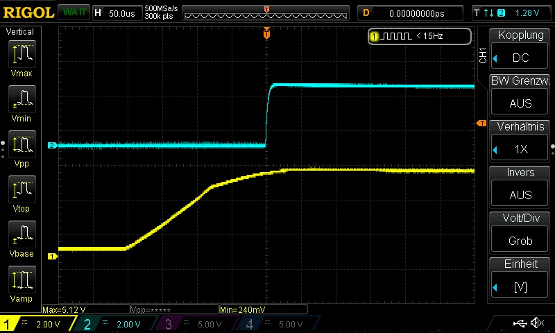
Output short circuit and recovery. Yellow is the output voltage, blus is /PG. Sadly I have no means to measure the current on the scope at this point, which might be interesting to to exactly measure the turnoff time. Looks acceptable though, no surprises.
1V25 from 3A to short 8.4V + recovery
5V from 1A to short 8.4V + recovery
3.5V from 1A to short 8.4V + recovery
All results so far are for the DCDC converters. The 1.75V and 2.5V LDOs were not tested. The ones on the regulator board are not even used, because currently they are included in the mainboard. The CHARGE input and charge_detect were not tested yet, I will probably do it when I have a SysCon PCB.
Here I’m documenting the used equipment for future reference:
| Power supply | Korad KA3005D |
| Vin measurement | Fluke 115 |
| Iin measurement | Fluke 87 |
| Vout measurement | HP 34401A |
| Electronic load + Iout measurement | Maynuo M9711 |
(Boring stuff ends here)
Well, if you managed to get this far through all the boring stuff, let's ask the interesting questions:
- What's the power consumption of the real system?
- How does it compare to the old regulators?
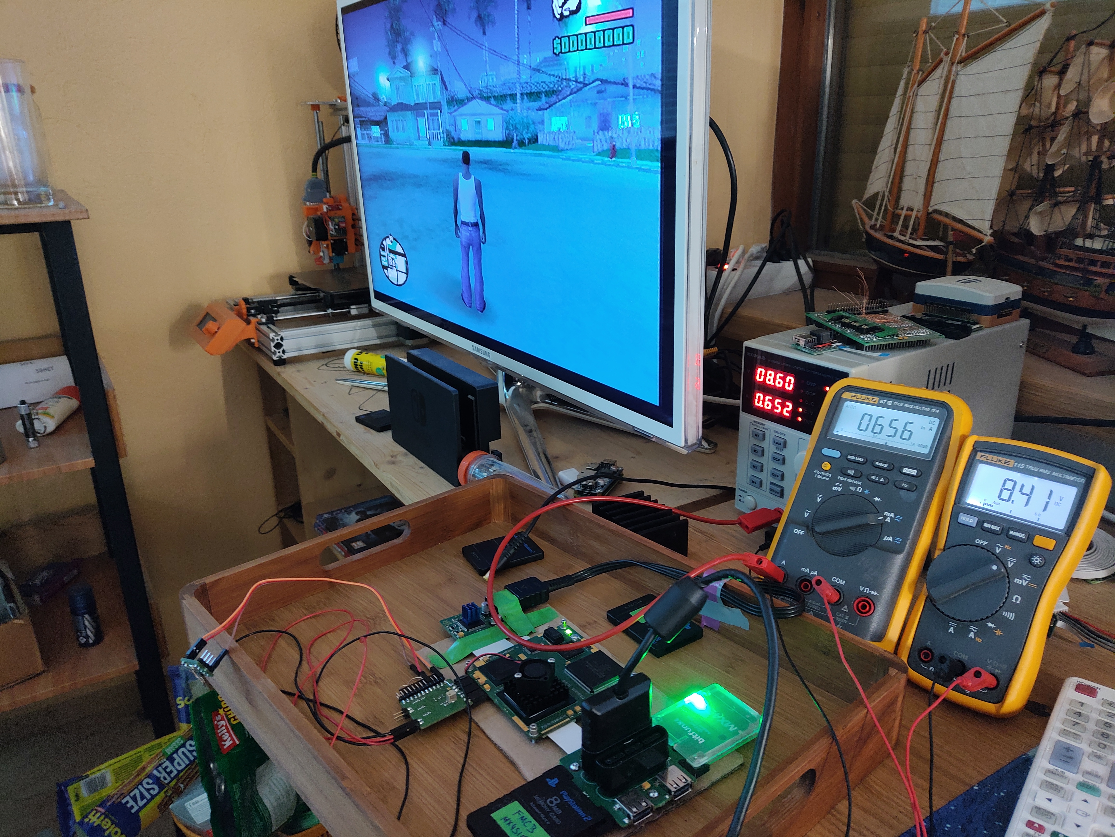
| Power consumption at 8.4Vin | [W] | Reduction [%] |
| old regulators (with FMCB, MX4SIO, DS2, fan) 1,25Vout GTA SA | 9.59 | - |
| new regulators (with FMCB, MX4SIO, DS2, fan) 1,25Vout GTA SA | 7.22 | -24.7 |
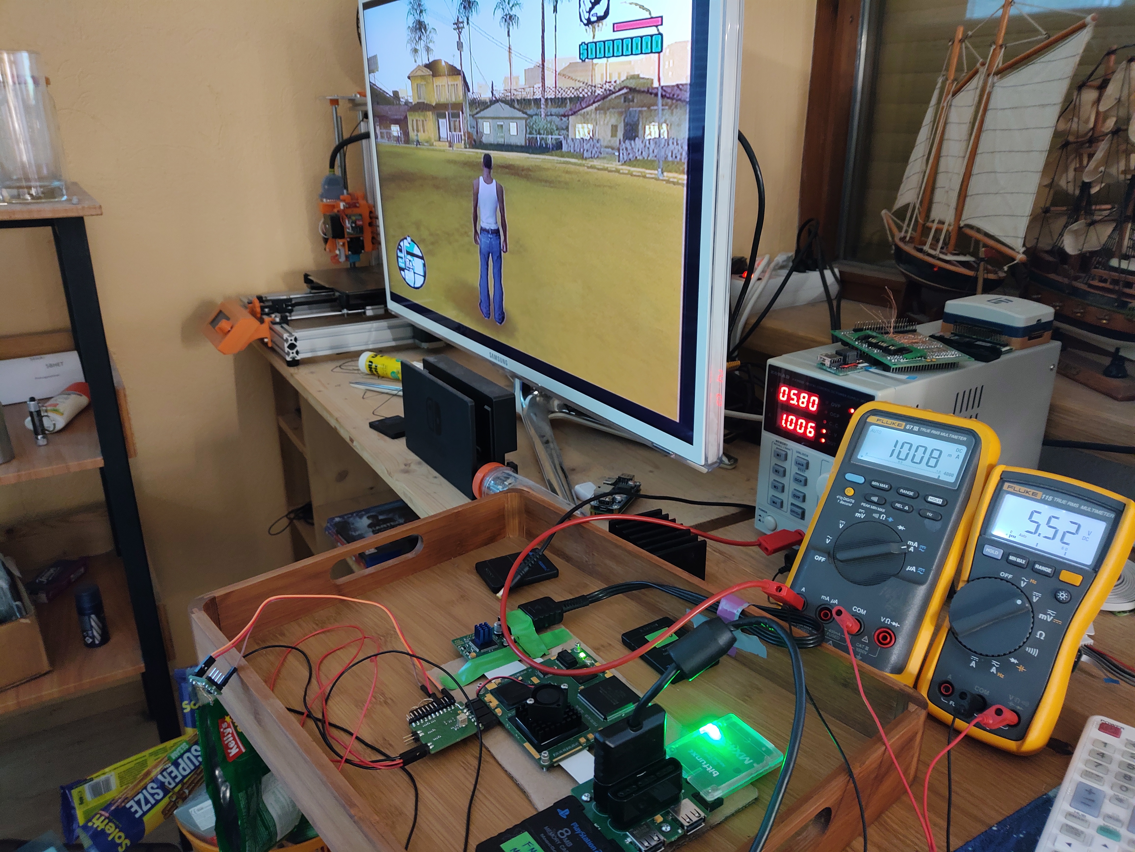
| new regulators (with FMCB, MX4SIO, DS2, fan) 1Vout GTA SA | 5.52 | -42.44 |
| Power consumption at 5.5Vin | [W] | Reduction [%] |
| old regulators (with FMCB, MX4SIO, DS2, fan) 1,25Vout GTA SA | 9.44 | - |
| new regulators (with FMCB, MX4SIO, DS2, fan) 1,25Vout GTA SA | 7.18 | -23.94 |
| new regulators (with FMCB, MX4SIO, DS2, fan) 1Vout GTA SA | 5.56 | -41.1 |
That outcome was unexpected! I double, triple and quadruple checked the measurement and it’s true! 5.5W, now we're playing in the Raspberry Pi league! If I didn’t include the pictures, I wouldn’t believe it myself. We went from 9.5W to 5.5W, -42%!
How did I achieve this? There is a hint in the table already, let me explain:
Mister M suggested to try undervolting the EE and that’s exactly what I did in the last row of both tables. I can only undervolt the EE and GS at the same time, because they are supplied by the same 1.25V rail. Those measurements were done with a moderate 1V setting. I also tried going below 1V, but the system kept freezing at <0,9V. It would be a good idea to be a bit conservative here, as different batches/chips might have varying tolerances.
I’ve played GTA and Okami for about 2-3h now and the performance was rock-solid. Not a single crash or weird unexpected behavior.
The fact that I didn't kill this system already after all those tests is a real miracle, thank you Playstation gods for staying on my side!
Another neat thing to measure would be the impact of the core voltage on the package temperature (mainy on the EE, the GS runs cool anyway), but I don’t have any means to perform that measurement. The same is true for the regulator board; my calibrated finger measurement states that it gets hand-warm during operation, but it would be nice to know the exact temperature (change). Sound like a good occasion to finally buy a thermal camera! Any suggestions?
Next up: Battery Management
I will keep this one short, because the post is already quite long.
The schematic is almost finalized and I’m starting to think about the component placement. The current implementation is heavily inspired by my CM4 portable that I never finished.
The first prototype will most likely include:
- BQ25792 - battery charging, power path
- STUSB4500 USB C PD negotiation
- MAX17205G Fuel gauge, cell balancing, maybe protection
The BQ25792 is a bit overkill for my application, but maybe I will need it in the future (may reuse the power management for other projects I have in mind). It is very compact compared to other 2S solutions, because it includes all FETs in the package. The downside is that the package has a very odd pinout, no idea what they were thinking while defining it…
Currently there is no stock, but I should be able to get my hands on a couple ICs in about a month.
The STUSB4500 was mainly chosen because of its popularity and proven functionality + there is some stock again. Something like the IP2721 would have been an interesting alternative.
On the MAX17205G I still have some doubts. It is a pretty neat fuel gauge, because it includes optional cell balancing for 2S applications. The downside is that in this mode it only supports high-side battery protection chips and those are quite hard to find. The one I found (S-8253C/D) is actually pretty bad compared to the protection features of the MAX17205G.
Although the BQ25792 already includes various battery protection features, I have a bad feeling about removing the separate battery protector, which could be seen as the secondary means of protection. That’s why I had an idea to use the alert output of the MAX17205G to disconnect the battery pack using back-to-back P-CH MOSFETs (pretty much what a battery protector does). The conditions to trigger the alarm are very flexible and configured via I2C + they can be stored to NVM. Not 100% convinced that this will work, but I will include it in the first prototype. If it doesn’t work, I can always bridge those FETS and try something else. In the upcoming updates I will give more information (depending on the availability of the BQ25792)
Puhh that was a long one!
Last edited: