What's new

Worklog Some PS2 Project

Joined
Dec 25, 2022
Messages
41
Likes
394
Location
Landeck, Austria
Hi there!
This is my first post here! I’ve been a long-time lurker around this forum and finally decided to post some progress on my latest project, as I think it might also help other people working on PS2s.

What is this project about?
It is about creating a PS2 system with minimal size and component count for portabalizing.

Why am I working on this project?
I love doing battery powered electronics as a hobby and I am often working on emulation consoles based on Raspberry Pis in my spare time.

So, at the end of 2020 I started working on another portable featuring the new RPi CM4 and a PCIe SSD. Half a year later, the housing design was almost done and the mainboard was ready for a first prototyping run. Of course, that was just about the time when the component shortage hit, and all of a sudden there were no more USB C PD controllers, no more STM32, and most importantly: no more CM4s. After another 6 months of searching components, I got frustrated and gave up on the project.

Electronics as a hobby is no fun without building circuits, so I had to search for alternative projects that did not require new ICs. That’s where the idea of reverse engineering a PS2 started to materialize, as PS2 slims are available for 10 bucks and they already contain most components. Why a PS2? That was my first console as a kid and to this day it is still my favorite console, I have so many good memories playing those games.

I was thinking about whether or not to start that project for quite a while, but in April of this year I finally convinced myself to tackle it.

Overview:
Before I felt confident enough to set requirements for the project, I had to analyze and modify a working 79004 mainboard to get to know the architecture. From time to time also testing FMCB and playing games on it to verify the stability of the modded system (too much playing and not enough analyzing TBH…). I also studied the wonderful PS2 trimming guide and Mister M’s board scans & worklog to get a better understanding of the board. Huge thanks for making that information public, that saved a lot of time!

Knowing a bit more about the system's architecture, I had to set a few requirements for my project to keep me focused in the ~3h I have per week:
  • the new mainboard shall be able to run games from USB/Ethernet
  • the original layout shall be simplified and the component count minimized
  • it shall feature an embedded miniaturized FMCB memory card
  • it shall feature a compact memory card slot that is compatible with original memory cards
  • it shall feature a custom gamepad interface with at least 1 gamepad
  • it shall feature more advanced video output by directly reading the parallel RGB on the video DAC
From my job designing and testing electronics as development engineer at an unnamed medical company, I have the habit to pursue a rather conservative design approach. That means that I always try to make my prototypes as modular as possible, to test all subcircuits individually. That way, only known working circuits are connected together, which usually simplifies troubleshooting.

Following that method, I derived some tasks to work on from the requirements above:
  • design and test a miniaturized version of an original PS2 memory card to get me in the mood of reverse engineering
  • design and test a slim memory card socket for original memory cards
  • remove all unnecessary components from a working 79004 mainboard, so only the core components are left that are required to boot and to test the console
  • reverse engineer that modified 79004 mainboard and create readable schematics + optimize the BOM
  • do the layout of the mainboard in a modular manner to simplify testing
  • design and test an ethernet transformer circuit for the ethernet PHY, based on OTS magnetics
  • design and test a compact power management system that powers the mainboard and runs off batteries
  • design and test a custom board to handle gamepad inputs (probably starting with PS2+)
  • design and test a video processor for an external display that deinterlaces and scales the parallel RGB of the PS2
I soon realized how hard it is to find reasonably priced PS2 79004s here in central Europe, so I had to find alternatives for sourcing the components on the board. First, I was thinking about buying new old stock ICs from some shady Chinese suppliers, but none of them seem to have the BIOS ROM in stock. So even if I bought all ICs, I would still have to find 79004s to salvage the BIOS chip.
On top of that, the new old stock is very expensive. In an offer I got, the BOM cost for most chips on the mainboard was around 70 bucks and that did not even include the system clock PLL (next candidate for replacing...) and the BIOS chip. Compare that to the 10 bucks for a used console.
So that made me thinking about buying 90004 consoles with broken disk drives, as they are dirt cheap and nobody seems to like them, because of their limited softmodding capabilities.
After comparing the 79004 and 90004, it seems that they are virtually identical hardware-wise, just the BIOS is different.
So, I decided to put another requirement to my list:
  • I shall be able to source the components from either a 79004 or a 90004 console.
That leads to another task:
  • replace the original BIOS ROM with a reprogrammable one to support 90004 hardware. And boy that was fun, more later.
And with that explanation out of the way, I would like to share my progress so far.

PS2 mini memory card
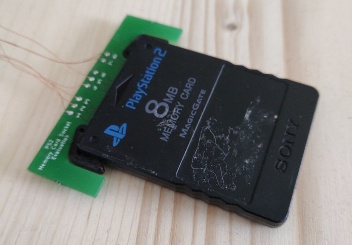
I spent 2 hours of my life trying to reverse engineer an 8MB memory card from Sony. The one I took was based on a CXD9585BR MagicGate ASIC.
The circuit I came up with should also work with other ASIC revisions, but I haven’t tested that yet. The only real difference I noticed comparing it to other memory card revisions is that on some of them, pin 24 is grounded and on some it’s left floating. On the board I made using the CXD9585BR, I left it floating.
The circuit is pretty straight forward, the only components required from an existing card are the ASIC and the flash. The flash can probably also be bought and programmed with an existing file system, but I haven’t bothered yet. All other components can be bought new, the trickiest one to find was the voltage supervisor driving the reset line. An LM809M3-2.63 did the job in the end. The board itself is a bit bigger than the flash itself (the flash is on the bottom layer) and it’s just a simple 4-layer module for testing. The final module will probably look different, but the circuit is functional.
Here some pictures of the design:
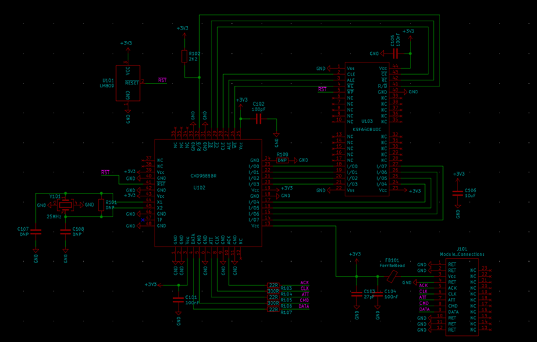
1672083279114.png
1672083308654.png


Slim memory card socket
Because I hate cutting the controller/memory card port into pieces to get a single socket for a memory card, I had the idea of making a custom socket. That also enables me to make the socket a bit thinner in the process. I came up with a pretty cool little socket by misusing some TE 1447360-8 as contacts. It can be flat with the PCB and just needs a small 3D printed piece (that can be integrated into a housing to save space) as locking mechanism. The whole assembly is actually half as thick as the actual memory card.
It survived at least 100 mating cycles already, but I think it still needs some work. I would like to make the PCB thinner, so the contacts are not that close to their min working range + a cover around the contacts would be nice to give them a bit more protection.
1672083402437.png
1672083408292.png


Reprogrammable BIOS
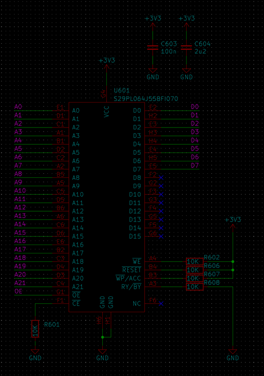
That was an adventure. I have spent the last 3 months to get that working. First thing to find out was the correct pinout of that ROM, so I dumped a ROM from a donor board as reference, took a couple of shift registers and an ESP32 to build a circuit that can read the chip and print the contents to the console.
1672083456551.png

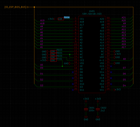
I also got some inspiration from the SCPH-7000 service manual and was hoping that the pinout would be identical. And surprise, it mostly is. At that point, only pins 12, 13, 14 and 15 were mystery pins to me. And was do we do with mystery pins? Yes, disconnect and see whether or not it still works. Not only was I able to read the contents of the chip correctly in that process, I also found out that you can disconnect pins 1, 12, 13, 14, 15 + the upper data byte and the chip still outputs the correct data. To be on the safe side, I pulled pin 1 up and pulled pins 12, 13, 14 and 15 down. The upper data byte can be left floating I guess.

That eliminated all my uncertainties about driving the ROM and the only pins required are OE, D0-D7 and A0-A21. That’s perfect for retrofitting an OTS flash. I also verified the functionality on a 79004 mainboard after removing all those pins.

So, the next step was to choose a suitable replacement. After hooking up the logic analyzer, I knew that the OE LOW time was min. 120ns and assuming that the PS2 latches the data in the center of the pulse (just assuming, because the interface is asynchronous), I would need an access time of MAX 60ns. That is quite fast, as most parallel flash chips today are only rated at 70ns+. Then I ordered 3 chips that were available (thank you chip shortage):
  • MX29LV320ETTI-70G at 70ns; probably not working
  • S29JL032J60TFI010 at 60ns; could be close
  • S29PL064J55BFI070 at 55ns; might be promising
While waiting for the order, I designed a couple of adapter boards and ordered a TL866 for programming the chips. Then testing started…

Long story short, the MX29LV320ETTI-70G and the S29JL032J60TFI010 did not work, probably because they are just too slow (as expected, kind of). The MX29LV320ETTI-70G only showed a black screen and the S29JL032J60TFI010 did boot, even into FMCB, but the firmware had some weird bugs, as if some bits were flipped while reading. To try and compare the speeds, I piggybacked the original ROM on top of the new ones and left the data pins disconnected. The logic analyzer showed a clear win for the original ROM regarding the access time.

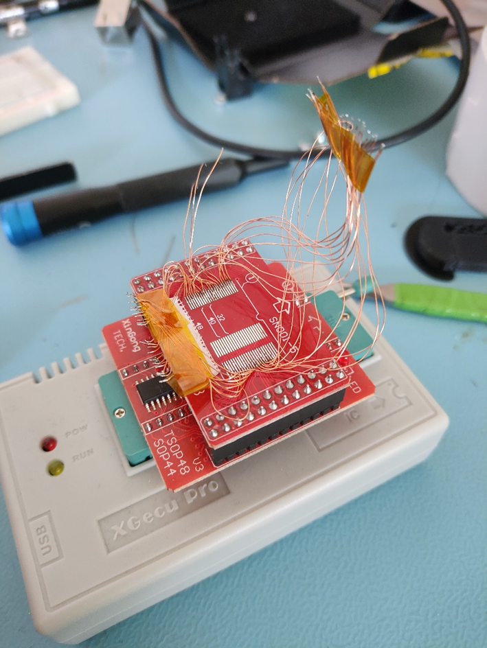
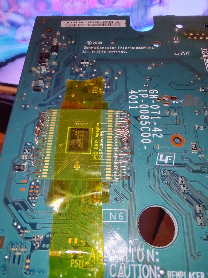
Then came my last try with the S29PL064J55BFI070. It was a bit more difficult to do the testing, because it’s a BGA-48 chip and its 4Mx16 instead of the 4Mx8 the PS2 needs. To be on the safe side, I’ve written a little program that inserts 8 zeros in the high byte of every address in the dumped 79004 BIOS to make the file 4Mx16. Flashing it involved a ratsnest of wires, because cheap me refused to buy the BGA-48 adapter for the TL866.
The fact that the S29PL064J55BFI070 is apparently not listed in the supported flash chips did not make it easier. But all that effort was worth it, IT BOOTS, the patient is alive. The PS2 90004 boots into FMCB and can play games from USB and ethernet. That means it works, at least for the sample size of 1 that I’ve got. Let's hope for now that I did not just get a good batch of flash chips and that it will also work on others.
1672083613268.png
1672083740101.png

1672083686306.png
1672083703970.png
1672083716551.png

And I’m not soldering another one anytime soon. I have 3 chips left and when trying to order more after that success, they were sold out; 39-week leadtime - thank you chip shortage. 3 chips for the next 39+ weeks, that flash will most likely be incorporated in a module I can reuse, in case there is no replacement for it.

PLEASE, if anyone can give any hints or suggestions on where to buy the S29PL064J55BFI070, or an equivalent alternative, I would really appreciate that. Because that is the only flash with 55ns access time that I was able to find.

Ethernet
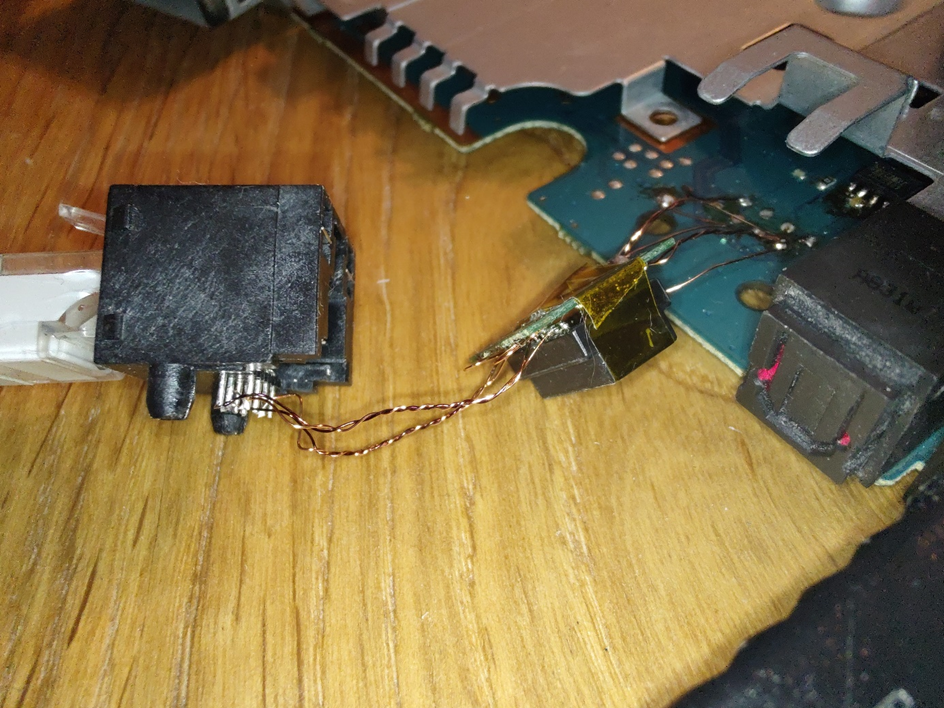
I think the picture says it all. Not very exciting. I replaced the transformer inside the ethernet jack with something you can actually buy today (Würth 749013011A). The circuit is now similar to the one found on the GH-061-51 mainboard. I verified it by playing my favorite PS2 game Okami for far too long via SMB. The only thing I hate about the transformer I used is the height – that thing is like a skyscraper, but it will do for now.
1672083797561.png
1672083802006.png

1672083819615.png


Modified mainboard and reverse engineering
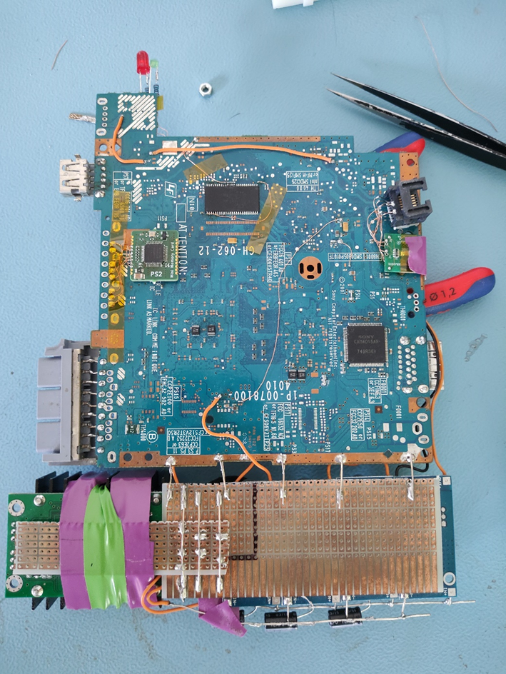
Oh, that poor GH-062-12 had to go through A LOT. I started removing components until the console didn’t boot and ended up with most components removed. Also desoldered and resoldered most passives to get the values. The power supply is now composed of 5 buck converters from amazon for 5V, 3V5, 2V5, 1V75 and 1V25. What? You’re asking why the 1V25 one is so huge and taped to the board? Because its predecessor couldn’t handle the load and released some magic smoke during an intense NFSMW session.
1672083850975.png
1672083971351.png

On that board you can also see the mini memory card in action, flashed with FMCB and ready to go. The audio codec was also successfully swapped with the CS4335-KSZ from mouser.
Not much more to tell about that board, so I will give you and overview of the schematics. I tried to make them as easy to read as possible, but there is still some room for improvement.
1672084006863.png


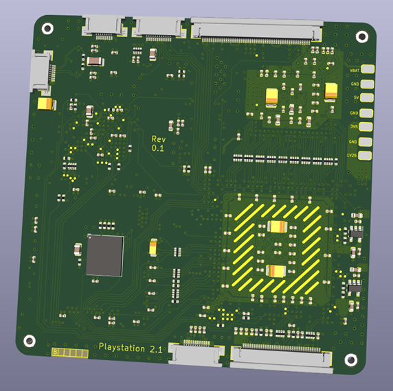
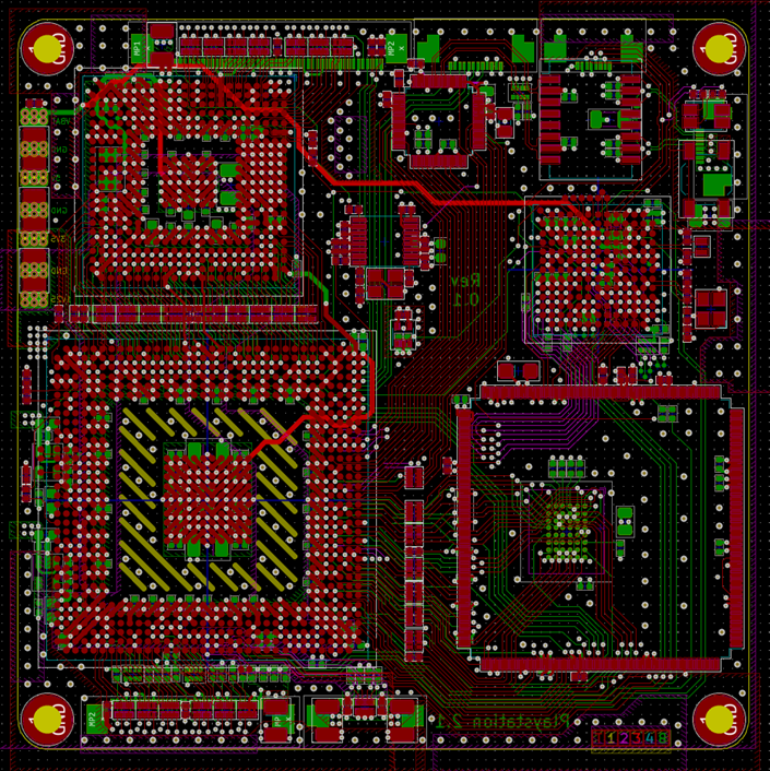
Layout of the mainboard (first prototype)
The board is currently 80x80mm in size and features 6 layers for improved signal integrity. I went with the following stackup: SIG – GND - PWR/SIG - PWR/SIG – GND - SIG at 1,6mm. The prepreg in the center is the thickest to reduce coupling between the 2 PWR layers.
The connectivity of the layout should be identical to my stripped-down mainboard, but I’m still in the process of cross checking the connections. The first prototype only provides the core functionality for booting, that means EE, GS, DSP, Mechacon, BIOS chip, ethernet PHY and the system clock PLL. The video DAC, audio codec, power management, connectors for USB gamepads, memory cards, ethernet will be external and are connected using ffcs. Currently, the board still includes the new flash, but I will mount it on a module for the upcoming prototypes, until I can source them reliably. The boards will most likely be manufactured at Aisler, as the price is reasonable at 14€ per piece (6 layers!!) and they are manufactured in Europe.
1672084134605.png
1672084064928.png

1672084203773.png


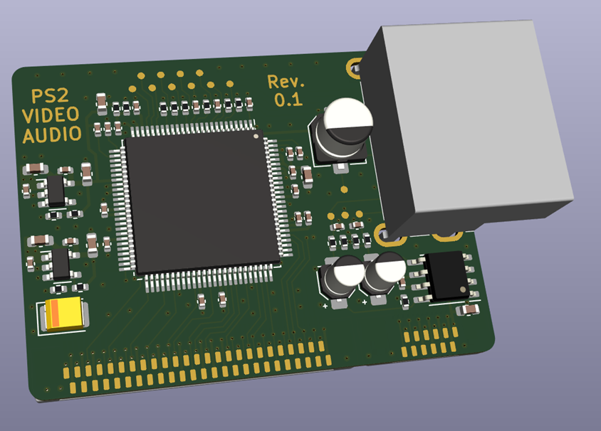
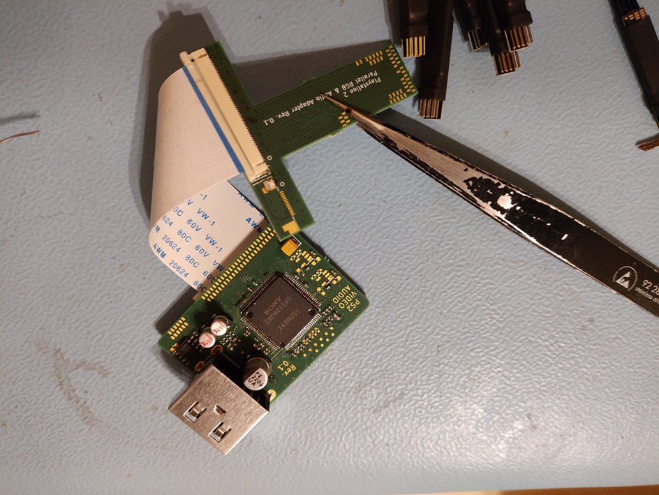
In parallel to the mainboard, I am also designing the video+audio relocation to test the first prototype. That enables me to take that circuitry off the mainboard and to swap it with a custom video processor later. I wasn’t sure whether or not that relocation would work, as the pixel clock is quite high at ~55MHz and I left the terminations only on the mainboard.
That’s easy to find out though, I can just make a small adapter to connect to an existing console and connect my video relocation from there. Then I have a known working video output for the new mainboard design. The board is 90% prototyped and almost ready for testing. Stupid me just forgot to order the small ffc socket, the LDOs and some caps. I could hook it up like this, but I’ll wait until I have all the parts. In the following picture you can see the current status of the board:
1672084281827.png
1672084353480.png


Prototyping the mainboard
Hopefully soon! I have most of the reballing equipment and most components ready. Any recommendations for good flux?
What’s keeping me from ordering the boards:
  • Verifying the functionality of the video DAC relocation
  • Designing a reusable module for my precious flash
  • Finishing cross-checking the design with the real deal
Also on the to-do list: power management, gamepad interface, video processor (some progress was made, but not noteworthy)

I could continue writing about the progress for another couple of pages, but I think I'll have to stop it here. Looking at that big chunk of text, I should have probably started posting my progress earlier. Hopefully it's not too hard to read, but I hope that might help some people with their PS2 projects. I would also like to apologize in case some of the pictures are messed up, I have honestly never posted on a forum before. Also sorry in case some things are hard to understand, I'm not a native english speaker in the end, but I'm trying my best.
I will try to keep the thread updated when there is notable progress to report.
 

thedrew

.
.
Joined
Sep 27, 2016
Messages
452
Likes
1,026
Shoot... well welcome to the forums! This is quite impressive and very ambitious. Thanks for sharing all your info with us. Looking forward to how this progresses!
 

Rvert

.
Joined
Jan 16, 2017
Messages
1
Likes
0
Very impressive, I am looking forward to seeing the working prototype. Are you planning on releasing the schematic and PCB layout in the future?
 
Joined
Apr 6, 2020
Messages
104
Likes
290
Hi there!
This is my first post here! I’ve been a long-time lurker around this forum and finally decided to post some progress on my latest project, as I think it might also help other people working on PS2s.

What is this project about?
It is about creating a PS2 system with minimal size and component count for portabalizing.

Why am I working on this project?
I love doing battery powered electronics as a hobby and I am often working on emulation consoles based on Raspberry Pis in my spare time.

So, at the end of 2020 I started working on another portable featuring the new RPi CM4 and a PCIe SSD. Half a year later, the housing design was almost done and the mainboard was ready for a first prototyping run. Of course, that was just about the time when the component shortage hit, and all of a sudden there were no more USB C PD controllers, no more STM32, and most importantly: no more CM4s. After another 6 months of searching components, I got frustrated and gave up on the project.

Electronics as a hobby is no fun without building circuits, so I had to search for alternative projects that did not require new ICs. That’s where the idea of reverse engineering a PS2 started to materialize, as PS2 slims are available for 10 bucks and they already contain most components. Why a PS2? That was my first console as a kid and to this day it is still my favorite console, I have so many good memories playing those games.

I was thinking about whether or not to start that project for quite a while, but in April of this year I finally convinced myself to tackle it.

Overview:
Before I felt confident enough to set requirements for the project, I had to analyze and modify a working 79004 mainboard to get to know the architecture. From time to time also testing FMCB and playing games on it to verify the stability of the modded system (too much playing and not enough analyzing TBH…). I also studied the wonderful PS2 trimming guide and Mister M’s board scans & worklog to get a better understanding of the board. Huge thanks for making that information public, that saved a lot of time!

Knowing a bit more about the system's architecture, I had to set a few requirements for my project to keep me focused in the ~3h I have per week:
  • the new mainboard shall be able to run games from USB/Ethernet
  • the original layout shall be simplified and the component count minimized
  • it shall feature an embedded miniaturized FMCB memory card
  • it shall feature a compact memory card slot that is compatible with original memory cards
  • it shall feature a custom gamepad interface with at least 1 gamepad
  • it shall feature more advanced video output by directly reading the parallel RGB on the video DAC
From my job designing and testing electronics as development engineer at an unnamed medical company, I have the habit to pursue a rather conservative design approach. That means that I always try to make my prototypes as modular as possible, to test all subcircuits individually. That way, only known working circuits are connected together, which usually simplifies troubleshooting.

Following that method, I derived some tasks to work on from the requirements above:
  • design and test a miniaturized version of an original PS2 memory card to get me in the mood of reverse engineering
  • design and test a slim memory card socket for original memory cards
  • remove all unnecessary components from a working 79004 mainboard, so only the core components are left that are required to boot and to test the console
  • reverse engineer that modified 79004 mainboard and create readable schematics + optimize the BOM
  • do the layout of the mainboard in a modular manner to simplify testing
  • design and test an ethernet transformer circuit for the ethernet PHY, based on OTS magnetics
  • design and test a compact power management system that powers the mainboard and runs off batteries
  • design and test a custom board to handle gamepad inputs (probably starting with PS2+)
  • design and test a video processor for an external display that deinterlaces and scales the parallel RGB of the PS2
I soon realized how hard it is to find reasonably priced PS2 79004s here in central Europe, so I had to find alternatives for sourcing the components on the board. First, I was thinking about buying new old stock ICs from some shady Chinese suppliers, but none of them seem to have the BIOS ROM in stock. So even if I bought all ICs, I would still have to find 79004s to salvage the BIOS chip.
On top of that, the new old stock is very expensive. In an offer I got, the BOM cost for most chips on the mainboard was around 70 bucks and that did not even include the system clock PLL (next candidate for replacing...) and the BIOS chip. Compare that to the 10 bucks for a used console.
So that made me thinking about buying 90004 consoles with broken disk drives, as they are dirt cheap and nobody seems to like them, because of their limited softmodding capabilities.
After comparing the 79004 and 90004, it seems that they are virtually identical hardware-wise, just the BIOS is different.
So, I decided to put another requirement to my list:
  • I shall be able to source the components from either a 79004 or a 90004 console.
That leads to another task:
  • replace the original BIOS ROM with a reprogrammable one to support 90004 hardware. And boy that was fun, more later.
And with that explanation out of the way, I would like to share my progress so far.

PS2 mini memory card
I spent 2 hours of my life trying to reverse engineer an 8MB memory card from Sony. The one I took was based on a CXD9585BR MagicGate ASIC.
The circuit I came up with should also work with other ASIC revisions, but I haven’t tested that yet. The only real difference I noticed comparing it to other memory card revisions is that on some of them, pin 24 is grounded and on some it’s left floating. On the board I made using the CXD9585BR, I left it floating.
The circuit is pretty straight forward, the only components required from an existing card are the ASIC and the flash. The flash can probably also be bought and programmed with an existing file system, but I haven’t bothered yet. All other components can be bought new, the trickiest one to find was the voltage supervisor driving the reset line. An LM809M3-2.63 did the job in the end. The board itself is a bit bigger than the flash itself (the flash is on the bottom layer) and it’s just a simple 4-layer module for testing. The final module will probably look different, but the circuit is functional.
Here some pictures of the design:
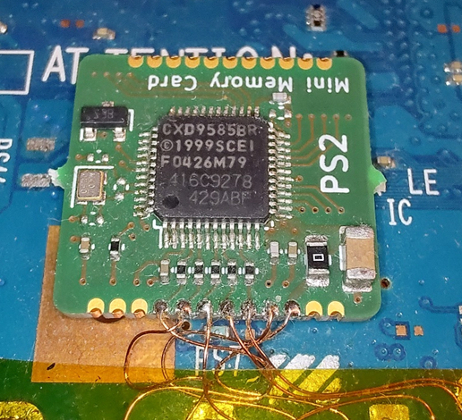
View attachment 25639View attachment 25640

Slim memory card socket
Because I hate cutting the controller/memory card port into pieces to get a single socket for a memory card, I had the idea of making a custom socket. That also enables me to make the socket a bit thinner in the process. I came up with a pretty cool little socket by misusing some TE 1447360-8 as contacts. It can be flat with the PCB and just needs a small 3D printed piece (that can be integrated into a housing to save space) as locking mechanism. The whole assembly is actually half as thick as the actual memory card.
It survived at least 100 mating cycles already, but I think it still needs some work. I would like to make the PCB thinner, so the contacts are not that close to their min working range + a cover around the contacts would be nice to give them a bit more protection.
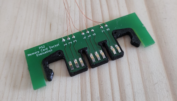
View attachment 25641View attachment 25642

Reprogrammable BIOS
That was an adventure. I have spent the last 3 months to get that working. First thing to find out was the correct pinout of that ROM, so I dumped a ROM from a donor board as reference, took a couple of shift registers and an ESP32 to build a circuit that can read the chip and print the contents to the console.
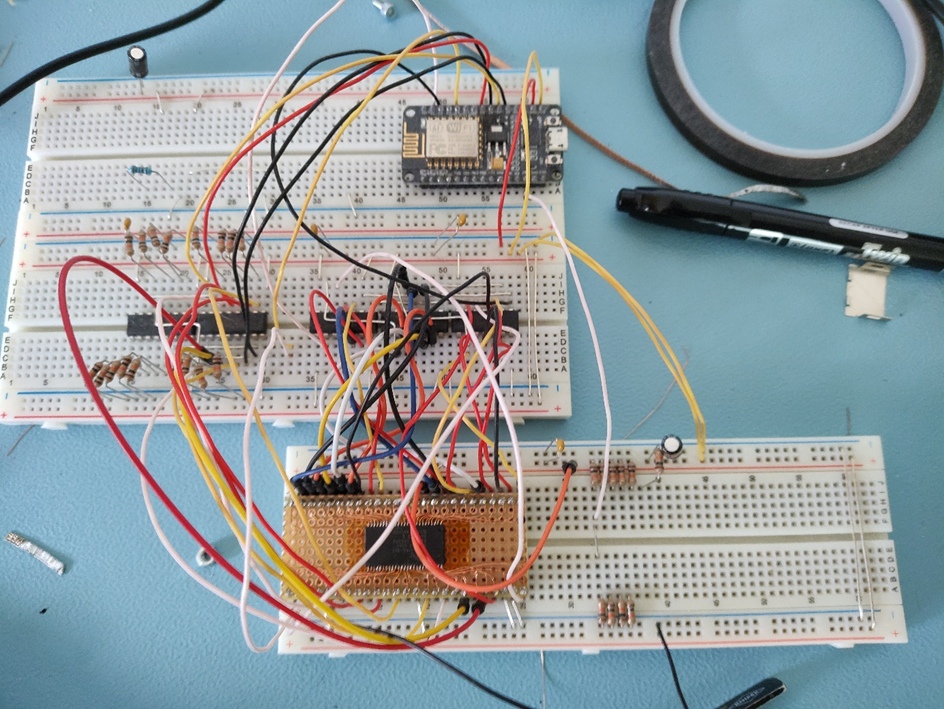
View attachment 25643
I also got some inspiration from the SCPH-7000 service manual and was hoping that the pinout would be identical. And surprise, it mostly is. At that point, only pins 12, 13, 14 and 15 were mystery pins to me. And was do we do with mystery pins? Yes, disconnect and see whether or not it still works. Not only was I able to read the contents of the chip correctly in that process, I also found out that you can disconnect pins 1, 12, 13, 14, 15 + the upper data byte and the chip still outputs the correct data. To be on the safe side, I pulled pin 1 up and pulled pins 12, 13, 14 and 15 down. The upper data byte can be left floating I guess.

That eliminated all my uncertainties about driving the ROM and the only pins required are OE, D0-D7 and A0-A21. That’s perfect for retrofitting an OTS flash. I also verified the functionality on a 79004 mainboard after removing all those pins.

So, the next step was to choose a suitable replacement. After hooking up the logic analyzer, I knew that the OE LOW time was min. 120ns and assuming that the PS2 latches the data in the center of the pulse (just assuming, because the interface is asynchronous), I would need an access time of MAX 60ns. That is quite fast, as most parallel flash chips today are only rated at 70ns+. Then I ordered 3 chips that were available (thank you chip shortage):
  • MX29LV320ETTI-70G at 70ns; probably not working
  • S29JL032J60TFI010 at 60ns; could be close
  • S29PL064J55BFI070 at 55ns; might be promising
While waiting for the order, I designed a couple of adapter boards and ordered a TL866 for programming the chips. Then testing started…

Long story short, the MX29LV320ETTI-70G and the S29JL032J60TFI010 did not work, probably because they are just too slow (as expected, kind of). The MX29LV320ETTI-70G only showed a black screen and the S29JL032J60TFI010 did boot, even into FMCB, but the firmware had some weird bugs, as if some bits were flipped while reading. To try and compare the speeds, I piggybacked the original ROM on top of the new ones and left the data pins disconnected. The logic analyzer showed a clear win for the original ROM regarding the access time.

Then came my last try with the S29PL064J55BFI070. It was a bit more difficult to do the testing, because it’s a BGA-48 chip and its 4Mx16 instead of the 4Mx8 the PS2 needs. To be on the safe side, I’ve written a little program that inserts 8 zeros in the high byte of every address in the dumped 79004 BIOS to make the file 4Mx16. Flashing it involved a ratsnest of wires, because cheap me refused to buy the BGA-48 adapter for the TL866.
The fact that the S29PL064J55BFI070 is apparently not listed in the supported flash chips did not make it easier. But all that effort was worth it, IT BOOTS, the patient is alive. The PS2 90004 boots into FMCB and can play games from USB and ethernet. That means it works, at least for the sample size of 1 that I’ve got. Let's hope for now that I did not just get a good batch of flash chips and that it will also work on others.
View attachment 25644View attachment 25648
View attachment 25645View attachment 25646View attachment 25647
And I’m not soldering another one anytime soon. I have 3 chips left and when trying to order more after that success, they were sold out; 39-week leadtime - thank you chip shortage. 3 chips for the next 39+ weeks, that flash will most likely be incorporated in a module I can reuse, in case there is no replacement for it.

PLEASE, if anyone can give any hints or suggestions on where to buy the S29PL064J55BFI070, or an equivalent alternative, I would really appreciate that. Because that is the only flash with 55ns access time that I was able to find.

Ethernet
I think the picture says it all. Not very exciting. I replaced the transformer inside the ethernet jack with something you can actually buy today (Würth 749013011A). The circuit is now similar to the one found on the GH-061-51 mainboard. I verified it by playing my favorite PS2 game Okami for far too long via SMB. The only thing I hate about the transformer I used is the height – that thing is like a skyscraper, but it will do for now.
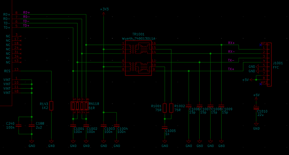
View attachment 25649View attachment 25650
View attachment 25651

Modified mainboard and reverse engineering
Oh, that poor GH-062-12 had to go through A LOT. I started removing components until the console didn’t boot and ended up with most components removed. Also desoldered and resoldered most passives to get the values. The power supply is now composed of 5 buck converters from amazon for 5V, 3V5, 2V5, 1V75 and 1V25. What? You’re asking why the 1V25 one is so huge and taped to the board? Because its predecessor couldn’t handle the load and released some magic smoke during an intense NFSMW session.
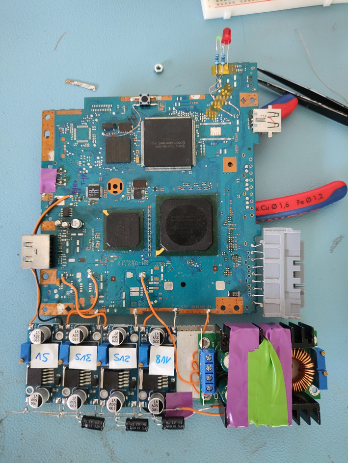
View attachment 25652View attachment 25654
On that board you can also see the mini memory card in action, flashed with FMCB and ready to go. The audio codec was also successfully swapped with the CS4335-KSZ from mouser.
Not much more to tell about that board, so I will give you and overview of the schematics. I tried to make them as easy to read as possible, but there is still some room for improvement.
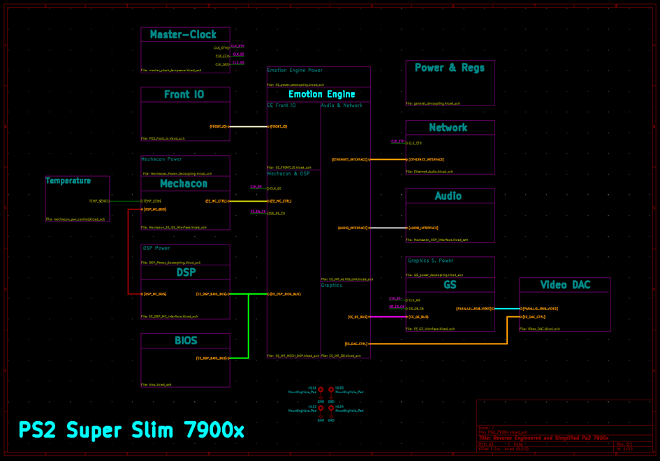
View attachment 25655

Layout of the mainboard (first prototype)
The board is currently 80x80mm in size and features 6 layers for improved signal integrity. I went with the following stackup: SIG – GND - PWR/SIG - PWR/SIG – GND - SIG at 1,6mm. The prepreg in the center is the thickest to reduce coupling between the 2 PWR layers.
The connectivity of the layout should be identical to my stripped-down mainboard, but I’m still in the process of cross checking the connections. The first prototype only provides the core functionality for booting, that means EE, GS, DSP, Mechacon, BIOS chip, ethernet PHY and the system clock PLL. The video DAC, audio codec, power management, connectors for USB gamepads, memory cards, ethernet will be external and are connected using ffcs. Currently, the board still includes the new flash, but I will mount it on a module for the upcoming prototypes, until I can source them reliably. The boards will most likely be manufactured at Aisler, as the price is reasonable at 14€ per piece (6 layers!!) and they are manufactured in Europe.
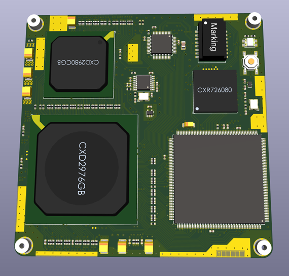
View attachment 25657View attachment 25656
View attachment 25658

In parallel to the mainboard, I am also designing the video+audio relocation to test the first prototype. That enables me to take that circuitry off the mainboard and to swap it with a custom video processor later. I wasn’t sure whether or not that relocation would work, as the pixel clock is quite high at ~55MHz and I left the terminations only on the mainboard.
That’s easy to find out though, I can just make a small adapter to connect to an existing console and connect my video relocation from there. Then I have a known working video output for the new mainboard design. The board is 90% prototyped and almost ready for testing. Stupid me just forgot to order the small ffc socket, the LDOs and some caps. I could hook it up like this, but I’ll wait until I have all the parts. In the following picture you can see the current status of the board:
View attachment 25659View attachment 25660

Prototyping the mainboard
Hopefully soon! I have most of the reballing equipment and most components ready. Any recommendations for good flux?
What’s keeping me from ordering the boards:
  • Verifying the functionality of the video DAC relocation
  • Designing a reusable module for my precious flash
  • Finishing cross-checking the design with the real deal
Also on the to-do list: power management, gamepad interface, video processor (some progress was made, but not noteworthy)

I could continue writing about the progress for another couple of pages, but I think I'll have to stop it here. Looking at that big chunk of text, I should have probably started posting my progress earlier. Hopefully it's not too hard to read, but I hope that might help some people with their PS2 projects. I would also like to apologize in case some of the pictures are messed up, I have honestly never posted on a forum before. Also sorry in case some things are hard to understand, I'm not a native english speaker in the end, but I'm trying my best.
I will try to keep the thread updated when there is notable progress to report.
An excellent project, and his knowledge of electronics is incredible. I'm happy to contribute in some way to the community and that it brings incredible results like this. We are both working on a similar project, if you want, I am available to exchange ideas and knowledge for the advancement of the portable PS2.
 
Joined
Dec 25, 2022
Messages
41
Likes
394
Location
Landeck, Austria
Very impressive, I am looking forward to seeing the working prototype. Are you planning on releasing the schematic and PCB layout in the future?
Yes, I am indeed planning to make the schematics and layout public, once I have a working board.

I may also release the modules I use for testing the mainboard (memory card, PMS, video/audio relocation, gamepad/memory card interface, ethernet module) as reference designs, in case there is enough interest.

But enough of that, let’s get to a quick update:

Video/Audio relocation
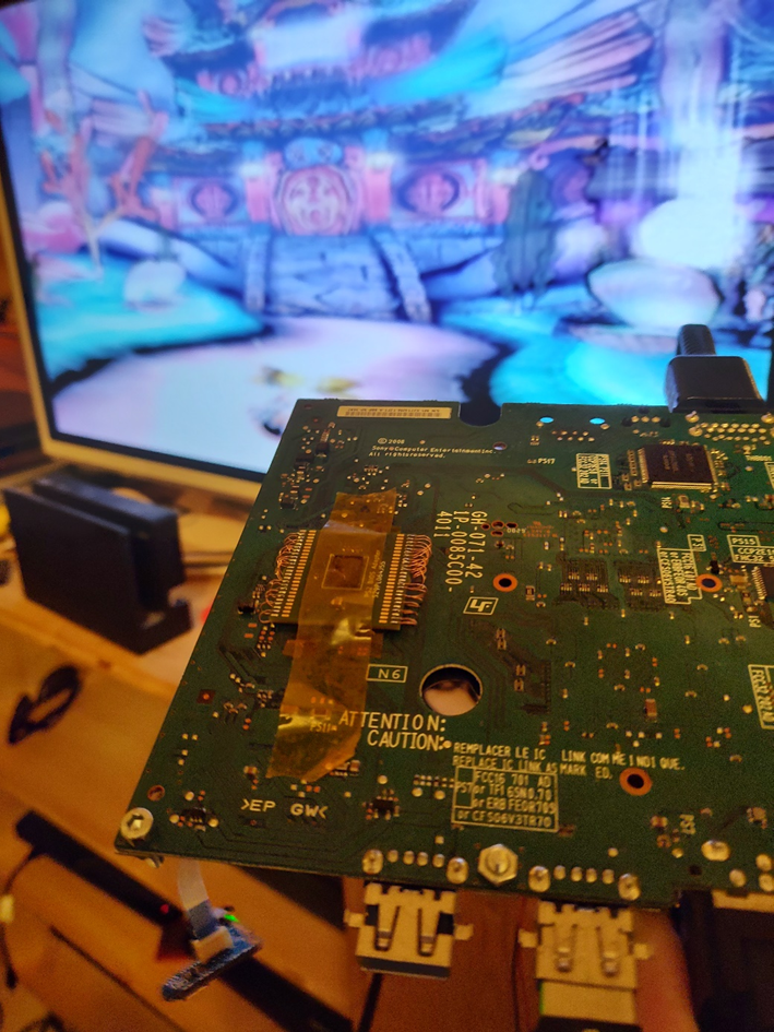
I may have the only GH-071-42 on the world that has 2 video connectors + a reprogrammable BIOS ROM, that thing looks so quirky now lol.

1673289286559.png
1673289325598.png

1673289353011.png

The missing parts arrived today and I was able to finish assembling the module. Then, after hooking everything up to the mainboard and checking for shorts, it was time to test it. The first try failed, there was video, but the colors were wrong. That led me to suspect a short/open line on one of the bits. So I checked continuity pin by pin and discovered that there was indeed a bit that was shorted to GND. It was a nasty short on one of the ffc sockets and it was so tiny that I was barely able to see it under 40x magnification.

After fixing that short, the relocation works now. So far, I’m not seeing any artifacts or instability, so I would call that module done. It will be used to test my custom mainboard, as there is no video output on the board.
1673289439947.png


Mainboard
I spent some time designing a module for the BIOS NOR flash, as I’m still unable to buy more. Now the BIOS plugs into the mainboard using 2 mezzanine connectors. The rated 30 mating cycles are not that great for testing, but I can live with that.
The module is already implemented in the layout and I was able to move a lot of the routing complexity from the mainboard to the module. That should also reduce the chances for manufacturing defects on the mainboard, as that flash has a ball pitch of 0,8mm and requires 0,2/0,47mm vias for the fanout, which is well below Aisler’s "official" capabilities. And I still refuse to order my PCBs from China.
1673289637261.png
1673289644808.png

1673289695430.png

What, it looks ugly and bulky? Yes, but it will save me enough time to be worth it. I only wish they had thinner stackups at Aisler. The 1,6mm will work, but 1mm or 1,2mm would be more than enough for this board.

Thinking about my wire spaghetti while programming the flash, I just had to design a programming adapter for the TL866 too. Both boards were ordered and I’m expecting them to arrive this week.
1673289794136.png


There was also some progress on cross-checking the layout. I did it the old-school way and compared every single pin on my GH-062-02 to the layout by measuring the connections using my multimeter (twice). Well, that took some time, all pads marked in blue were measured. But it was worth it in the end, because I found a stupid mistake on the \XHWR line. The rest of the layout matches my modified board, as far as I can tell.

1673289868098.png

The next step is cross-checking the footprints and then I think I am ready for ordering the first prototype.

If time allows, I may also
  • start designing an interface board for connecting memory cards and controllers (for testing purposes)
  • start designing a video adapter to connect my logic analyzer and FPGA development board
 

Fly_5

.
Joined
Apr 4, 2022
Messages
86
Likes
120
Location
Spain
Portables
Megadrive portable / PS2 Next-G portable
I'm glued to the laptop waiting for your new developments ... impressive work,congratulations.
 
Joined
Dec 25, 2022
Messages
41
Likes
394
Location
Landeck, Austria
Another small update!

My first point is probably a bit off-topic, but I think it might be interesting. In a conversation with Mister M I was made aware of a problem he has with custom regulators on the 90k mainboards. Apparently, the console always died when he tried to power it externally. I do have a couple spare 90004 mainboards here, so gave it a try myself, just for fun.

Long story short: It works and I would like to document the changes I made somewhere, before I forget what I did.

I first removed the motor driver and RF amp, because they were also not needed on the 79004 mainboard. Then I tried to find the regulators for the voltages, which is easier on this revision, because most LDOs are integrated in one PMIC next to the GS. I could find the standby 1V8 & 3V5, 1V8, DSP AVCC (3V5), 2V5 and the switched 8V5 there.
I also measured 5V and another 3,5V on that chip, but I suspect that they are inputs. The 5V on the PMIC is tied directly to the output of the LM7805 next to it and the 3,5V is tied directly to the output of the 3V5 DCDC.
Then there is the DCDC controller on the bottom for the 1V2 and 3V5, similar to the 79004. There are also 4 EN lines coming from the Mechacon. First I wanted to disable the power-on sequencing to see whether or not that would kill this revision. I did that by cutting the EN lines and connecting them to 3V5 SBY on the PMIC side. I’m not 100% sure, but they should be the EN for 1V2, 3V5, 1V8 and the switched 8V5.
After pulling the EN high, the mechacon had no control over the power management anymore and all regulators were running as soon as there was power. The console was still booting.
The next step was to prepare the board for external regulators by removing the DCDC controller, 3V5 MOSFET, 1V2 MOSFET, PMIC and the 3 LM7805s (one of them should be for the RF amp & audio codec and the other 2 for the USB & motor driver).
Then I connected a jumper wire between the outputs of the 3 LM7805. The next step was bridging the standby 1V8 to the 1V8 + the standby 3V5 to the 3V5. AVCC is not required for booting and can be floating. The switched 8V5 is also not needed anymore, as the motor driver & 5V regulators are gone.

Then it was time to connect my external regulators: 5V, 3V5, 2V5, 1V8. I also added bulk decoupling to the 1V2 and 3V5 input (just 100uF). After a quick check for shorts, I plugged it in and the red LED did not turn on. That was a bit scary, but I tried turning it on anyway – and it boots.
Afterwards I tried to find the reason why the LEDs stopped working and quickly found that the anode of both LEDs is tied to 8,5V. They are switched by the mechacon using a dual N-CH MOSFET on the opposite side of the eject ffc. My quick solution was to cut the 8V5 trace to the eject board and supply just that board with 8,5V from the input. A more elegant solution would be just to remove the N-CH MOSFET and hook the LEDs directly to the mechacon, just like I did on my modified 79004 and my custom mainboard.

I’m not planning to do much more on that board, of course you could remove a lot more components after that modification. Hopefully someone finds the information here useful and now I also have a reference for the future, in case I do that again. Please excuse the sloppy soldering in the pictures, that was really just a quick 2h job.

1673637719809.png
1673637746442.png

1673637774173.png
1673638507870.png


Now to the other small updates:

BIOS Module

I received the BIOS module and the programming adapter and managed to assemble both. After cleaning all the flux off the mezzanine connectors, I programmed it with my modified BIOS. I haven’t tried hooking it up to a mainboard, but reading it using the programmer gives me the correct binary back. Because of that, I assume for now that it works.
1673638015893.png
1673638024825.png


Reballing
Today I also tried my first reball on a spare (broken) EE chip. That was actually easier than expected, apart from melting the balls using hot air. For the balls not to fly away, I had to set the airflow to 10% and it took ages to melt the solder, even at 360°C. I am not comfortable with exposing the chips to such heat for too long, so I will have to find an alternative way of doing the heating... maybe my reflow oven that I'm designing as a small side project.

The rest was pretty straight forward – put tape on the unused holes in the stencil, clean the BGA and apply a thin layer of tacky flux, put the BGA in the holder and align the stencil, add the balls and shake until all holes are filled, carefully remove the stencil and double check that all balls are in place, heat up to melt the balls. Pretty pleased with the result, there are just 1 or 2 balls that look a bit crooked, presumably because they didn't melt fully.

If someone has tips or suggestions for improving my reballing process, I would appreciate that!

After trying a couple of ball sizes, I decided to go for 0,55mm Sn63/Pb37 balls. That also means that I will have to adjust the BGA pad diameters on my design to ~0,45mm. I plan to have the balls collapse on the pads, as the ball pitch is big enough. That means I will have to pull back the solder mask a bit more compared to the current design for optimal solderability.
1673638145280.png
1673638155669.png


Gamepad Test-module
Then the last update: today I received these fancy female PS2 gamepad sockets from aliexpress. I’m planning to incorporate them into a simple little memory card & gamepad test module that connects to my mainboard via the front IO ffc. Now I can create a footprint and then start with the design of module soon.
1673639245488.png


Apart from that I am still working on checking all footprints and I hope to be finished with that this weekend.
 
Last edited:

Fly_5

.
Joined
Apr 4, 2022
Messages
86
Likes
120
Location
Spain
Portables
Megadrive portable / PS2 Next-G portable
Excellent work I will be attentive to your new post, congratulations
 
Joined
Dec 25, 2022
Messages
41
Likes
394
Location
Landeck, Austria
Update time!
A lot has happened since my last post. I will go over all my points and I would like to start with the BIOS.

Reprogrammable BIOS
I hopefully managed to drastically increase the stability and compatibility of my BIOS mod (don’t jinx it, I’m still in the testing phase!). Here’s the story:

Finally, one of my alternative flash chips (S29JL064J55TFI000) was back in stock and I couldn’t resist ordering a couple for testing. It is the faster version of the S29JL032J60TFI010 that I was testing previously and it has the benefit of being a TSOP-48 part too. It is a 64Mbit flash instead of the 32Mbit that I need, but grounding the MSB of the address does the job. (the MSB might also be interesting for having 2 different selectable BIOS in one chip...)
The whole flashing and soldering procedures were repeated aaaand… it worked mostly. Again, there were some weird bugs, but the console did boot. The issues were similar to the ones I found in the S29JL032J60TFI010. FMCB would freeze constantly and in the browser the console would always show “Reading Disc” (have fun waiting for the disk to read when there is no disk drive attached…). The fact that the specified access time is the same as my working flash chip made the situation a bit suspicious to me and forced me to do some more in-depth troubleshooting.

The "solution" started with a simple thought...
The “Reading Disk” does not sound like something that would be related to the BIOS, but more related to the DSP, as its responsible for reading the disks together with the Mechacon. I know that the DSP is sharing the same bus with the BIOS and then the issue dawned on me….

When swapping the ROM for the first time I had some concerns regarding the removal of the chip enable, but I assumed that both DSP and BIOS ROM have separate OE, which would prevent bus conflicts from happening. During testing the ROM also worked without the ROM CE connected, so I didn't continue testing in that direction. But after those strange errors on some chips I started second-guessing myself. I checked the schematics and found that the OE for both DSP and BIOS is connected to the same pin on the EE. The potential problem was in front of my nose all the time, but I didn’t bother to check, because some ROM chips were working without CE... The theory makes sense, when the ROM is enabled all the time and the EE tries to read something from the DSP using the same OE, there will be conflicts.

The first attempt to mitigate this potential issue was to try and use one of the mystery pins of the BIOS ROM as CE for the flash chip. I tried all of them, but the console wouldn’t boot with any of them connected to the CE of the flash. That was a dead end.
The fact that I cannot enable the flash when it should be enabled made me think of an alternate solution: disable the flash when the DSP is enabled. Thankfully there is a CE for the DSP that I can use to try that idea. I tried the following:
Connect the input of a 74LVC1G04 inverter I had in my junk bin to the DSP CE (pin 169) and connect the output to the CE of the flash chip. That way, only one of the 2 can be enabled at a time. And surprisingly that did the job. There are no weird bugs anymore and I also tried playing some games using FMCB. An added bonus is that the slower S29JL032J60TFI010 that didn’t work last time also works now.
1675366333344.png
1675366344662.png

Why did it work for the original ROM and the S29PL064J55BFI070? I can only assume that the output drive of these chips is just weak enough to let the DSP communicate, even though there are bus conflicts. Or maybe it’s just timing differences…
I will have to do more testing, but I think that was a good step in the right direction. Sadly my mainboard was in production already when I discovered this fix, that means I will have to retrofit that inverter onto the first prototype.

Mainboard Design
The mainboard of the first prototype was ordered and arrived yesterday. That was also harder than expected.

Shortly before ordering the PCB I found out about the new KiCad 7 and the amazing new features it provides. Usually, I try to avoid updating my software when I’m in the middle of a project, but the new teardrop manager totally convinced me. I just had to include teardrops in my design.
We use teardrops all the time at work to increase the reliability and the yield of our boards and its amazing that the new KiCad has a teardrop manager on par with the Altium equivalent that we use. It will especially help with the relatively small annular rings I have on my mainboard. KiCad 7 is not out yet, so I updated to the release candidate 1 and I’m very happy with it so far.
1675367296054.png

The only issue I had so far was the reality that KiCad 7 imports are not yet supported at Aisler. For uploading, I had to create the Gerbers manually. At work that’s not a big deal, we have tools to prepare, rename and inspect the files for our suppliers. At home on the other hand, it’s a real pain to rename like 10 files manually every time I export them. That’s why I always refused to do the Gerber export so far and used suppliers that take the design files directly. Now I was forced to work with Gerbers at home, so I took a couple of evenings to write a python script for renaming and zipping the files for the upload. Now it’s very convenient to export Gerbers quickly and with whatever name the supplier requires.
It would also enable me to conveniently order my boards from JLC now, I'm curious about their new via filling options. Epoxy filling & capping would be included on 6 layers, but copper filling still has a steep price gap. The epoxy filling is not suitable for my BGAs, but there would be some other places on the mainboard that would benefit from some "free" via-in-pads.

Now to the PCBs. As I mentioned already, they arrived yesterday and I am very pleased with the quality so far. I ordered 3 boards and received 9, that tells me that the manufacturer expected low yield and made more boards than ordered. Apparently, they did a good job and shipped the remaining ones too. The price is outstanding at 7,60€ per 6-layer board, including a stencil for top and bottom – it always amazes me how much the prices for PCBs have dropped in the last couple of years!
1675366571624.png
1675366584379.png

The most important footprints were cross-checked with the real components and so far, they all match! The next step would be the assembly, but I don’t think I have time in the next 2 weeks. I’m in the process of expanding my lab & soldering equipment and my desk is a complete mess right now. The components are all here and I will start with the assembly as soon as I get my things sorted out.

Another thing I did in the meantime to prepare for the assembly was to check whether my new crystals work. In that process I successfully swapped the 18,432MHz crystal with the 7M-18.432MEEQ-T, the 16,934MHz crystal with the NX3225GA-16.9344M-STD-CRG-2‎ and the RTC crystal with the ABS05-32.768KHZ-9-T. The new crystals are much smaller and the console still boots and plays games. I will, of course, keep an eye on the stability of the system, once I have it running.

1675366688905.png
1675366698276.png


The last update I have for the mainboard right now is my work on a custom "heatspreader". Some time ago I figured out that you can produce custom sheet metal parts using 3D printed molds. After some testing, I found that 0,5mm aluminum sheets work best for this method. Below you can see my first try making a heatspreader for the mainboard. I am still trying to optimize the process and I am also playing around with different designs. If I can get my hands on 0,5mm copper sheet metal, I would also like to try that. Then you would be able to solder heat sinks directly to the heatspreader.
1675366784773.png
1675366865633.png


Controller & Memory card breakout board
Another thing I will need for testing the mainboard is a breakout board for connecting controllers and memory cards. The design is almost finished and I will order the PCBs soon. It will contain the whole front IO of the PS2 and connect to my mainboard via the front IO ffc.
While doing the design I discovered a little oopsie on the ffc pinout that will require a bodge wire on the mainboard prototype. The 7V6 supply for the memory cards is present on the ffc, but I forgot to connect it on the mainboard. That’s not a big deal as the original memory cards are not using that supply, but I think some knockoff cards might not work. I also realized that I will need more 5V lines on the ffc in the next revision, but it’s no big deal either.
I decided against ESD diodes for now, as I don’t see any ESD problems during testing and that saves me some BOM items. There is also a pin header attached to controller port 1 for bus sniffing and hooking up a custom gamepad interface in the future. Another thing I adjusted was the custom memory card socket. I made the outline a bit simpler and simplified the design of the snap hooks.
My attempt to make the board as small and cheap as possible also led to a funky looking outline...
1675367015993.png
1675367095759.png

1675367115133.png


That's it for today!
 

YveltalGriffin

First Wii U Trimmer
.
Joined
Jun 7, 2016
Messages
378
Likes
1,609
Location
South Florida
Portables
5
This worklog has been an absolute joy to read! Really professional designs and great workmanship-- can't wait to see your assembly process. Clever idea to use an inverter on the DSP CE line!

Out of curiosity, why wouldn't nonconductive fill be suitable for the BGAs in your design? I was under the impression that conductive fill was intended for thermal vias. At least, that's the only scenario I've used them in at work (heatsink pads, ICs with exposed thermal paddles). Nonconductive fill for everything else.

Keep up the great work! :D
 

Fly_5

.
Joined
Apr 4, 2022
Messages
86
Likes
120
Location
Spain
Portables
Megadrive portable / PS2 Next-G portable
impressed with your work, I find it amazing, I will wait impatiently for your progress. incredible work, congratulations.
 
Joined
Dec 25, 2022
Messages
41
Likes
394
Location
Landeck, Austria
This worklog has been an absolute joy to read! Really professional designs and great workmanship-- can't wait to see your assembly process. Clever idea to use an inverter on the DSP CE line!

Out of curiosity, why wouldn't nonconductive fill be suitable for the BGAs in your design? I was under the impression that conductive fill was intended for thermal vias. At least, that's the only scenario I've used them in at work (heatsink pads, ICs with exposed thermal paddles). Nonconductive fill for everything else.

Keep up the great work! :D
I might be living in my company bubble when it comes to via filling. :?:
We mainly work with <0,4mm pitch WLCSP packages with laser drilled uvias and for that our assembly house reccomends conductive filling to improve the soldering process. Apparently they found that those pads are more planar than the epoxy filled vias in our application and with our PCB suppliers. I have also seen some poorly done epoxy filled via-in-pad with considerable "sink marks" before, that's why the conductive fill would have been my first choice.
You have a point, nowadays the epoxy filling is much more common and the preferred method. I have also heard that they handle temperature stresses much better due to the more optimal CTE. For our low power chips thats neglectable, but for the hot PS2 chips it will be a consideration. Thinking about it again, epoxy filling might indeed be the better option for the mainboard. I just wish I had a sample from the process at JLC. Maybe that's a good reason to order the next revision from JLC, then I know how they look!
 

StonedEdge

a.k.a. ClonedEdge
.
.
Joined
Nov 16, 2018
Messages
382
Likes
1,549
Location
Japan, Tokyo
Portables
2
This is fantastic stuff, I especially like the heatspreader idea. That PCB looks gorgeous. Best of luck with the BGAs too!

DC9E09C1-8718-4154-BA5B-6FF9F4568C3F.gif
 

YveltalGriffin

First Wii U Trimmer
.
Joined
Jun 7, 2016
Messages
378
Likes
1,609
Location
South Florida
Portables
5
I might be living in my company bubble when it comes to via filling. :?:
I have also seen some poorly done epoxy filled via-in-pad with considerable "sink marks" before
Right there with you, every place has their own preferred way to do things. Hopefully JLC's VIPPO is decent! The preview pics they post online do show dimples, so it's probably not quite as good as a big-time fabhouse. But hey, can't argue with free! :P
 
Joined
Dec 25, 2022
Messages
41
Likes
394
Location
Landeck, Austria
Update time!

3 weeks have passed since my last update and in this time, I went through engineering hell and back.

But the hard work was worth it, I am excited to announce that the first prototype of my custom PS2 mainboard finally boots! I literally managed to get it working 2h ago and the system was stable during a quick Okami session. Here it is:
1677442666195.png
1677442675279.png

(BTW: my temporary “cooling solution” managed to keep the EE pretty cool, don’t make fun of it! Also please ignore all the flux residue on the board, I call it "battle scars" from 2 weeks of troubleshooting...)
1677442704704.png
1677442772276.png


I assembled the board 2 weeks ago with components from my last 79004 mainboard. The reballing process was very smooth, maybe I can give some insight on how the process looked:

Reballing Process

The first step was to desolder the EE, GS, Mechacon, DSP, Ethernet PHY and System clock PLL and to clean them using solder wick. I did the desoldering using my IR preheater and hot air tool, that makes it a lot easier to melt the original lead-free solder. The temperature on the preheater was set to ~360°C and the hot air to 320°C, 90% airflow, that gave pe pretty good results without cooking the chips too much.
1677442829815.png
1677442860570.png

I can recommend to clean the pads of the BGAs very thoroughly using solder wick, that way the solder balls stay in place much nicer later on. It is also important to apply as little force as possible on the pads while cleaning. When that was done, I cleaned the flux residue on the 3 BGAs using 99% isopropanol.

With that preparation done, I continued to mask the unused holes in the stencil. I’m using a 0,55mm universal stencil with 1mm pitch. In case anyone has the same reballing fixation, I applied some kapton tape in 2 diagonal corners to prevent the lid from moving around too much, as the sloppy tolerances made the alignment really tricky.
1677442931086.png
1677443015471.png

The next step was to apply a thin layer of tacky flux on all pads of the BGA, I used my finger to spread it evenly. The BGA was mounted in the fixation and the stencil was aligned very carefully. The vertical alignment is also VERY important! If the distance between BGA and stencil is too big, the solder balls will not be aligned. If the distance is too small, the balls will not stay inside the holes and when they pop out, they will contaminate the top of the stencil and the other solder balls with flux. That causes the balls to get stuck in the stencil when lifting it off the BGA (which is a big pain, as those balls will have to be placed manually). Always clean the stencil after reballing!

When all balls are in place, I use the preheater and hot air again to melt them. I had good experiences with putting the BGA on an unused stencil and having it over the preheater (set to ~360°C). I usually set the hot air to 320°C, 10% airflow to not blow the balls away while heating. That way, I can slowly hover over all pads until all balls are soldered.
1677443120064.png
1677443161373.png

That’s the reballing procedure I followed for the EE, GS and Mechacon. One thing that really annoyed me was the fact that I only have one stencil. That means I have to mask the holes 3 times to reball the 3 chips. Having 3 stencils would save a lot of time, so I ordered new ones from aliexpress.

Placement

Next was the component placement. There is this fancy KiCad plugin called “Interactive HTML BOM” which exports the BOM and a visual guidance where to place the components on the board. Man, I love that thing and I whish Altium had something similar, it makes the component placement SO MUCH easier.

The first side to be populated was the bottom layer. I ordered a solder paste stencil together with the PCBs, so that was very straight forward. When all components on the bottom were placed, I put the board on the preheater again and soldered everything using hot air on a first reflow run.
After that, I put copper tape on the ffc sockets, the mezzanine connectors and the LDOs to prevent them from falling off during the second (top side) reflow.

Then I turned the board around and populated everything on top, except the 3 BGAs. When the top side was done, I put the board back on the preheater at 360°C. I applied a thin layer of flux on all BGA pads of the PCB and placed the BGAs on the PCB. At work, our PCBA assembly house usually does it the other way around – they dip the BGA balls in a low viscosity flux before placing them.

The alignment of the BGAs was very easy, because I have the exact size of the package outlined on the silkscreen – I would highly recommend that for hand-assembly.
Then it was just a matter of heating the board up to solder all components. The BGAs are usually a bit more difficult to observe without the right equipment, so I always give them the -tiniest- push and when they “float” back into position, the connections are good.
After slowly cooling down the CBA, I measured the resistances on all supply rails and they seemed OK.

1677443270364.png
1677443280698.png

1677443312054.png


Testing

That was the point where the fun started…

When powering the mainboard on for the first time, the red power LED turned on – so far so good. When pressing the reset button, the LED turned green, but the current consumption stayed at around 200mA. The board was completely dead, there was no video, no audio and not even bus activity on the EE-GS bus and the EE-DSP bus.

I compared most signals to a working board and saw that the EE was not even initializing when powering the board (with the red LED on).

On the good board, even before pushing the reset button, most signals between the EE, GS, DSP were initialized HIGH, the clocks for the EE, GS and ethernet PHY were present. The EE was outputting clocks for the DSP and for the GS. When pressing the reset button the console boots normally with bus activity everywhere.

On my board, a lot of the connections between the EE, GS and DSP were floating at around 0,3-0,6V. The respective clock signals for the EE, GS and ethernet PHY were present, so the system clock PLL was working. The EE did not output clock signals to the GS and the DSP. The CE and OE for the DSP/BIOS were floating at 0,3V, on the good board they were HIGH.
The GS did output a clock to the EE and the Mechacon also seemed to do its job – it tried to boot the system, tried to enable the supply rails and it was outputting a clock to the EE when pressing the reset button. What did not work, though, was turning the system off – it looked like the Mechacon was waiting for something.

These observations made me rule out the GS, clock PLL and Mechacon in my attempt to find the fault. The remaining suspects were the EE (highly sus), DSP and ethernet PHY. What made me rule out the DSP and ethernet PHY in the end was the fact that they were also doing nothing on the working mainboard, at least before pressing the power button. Everything that was supposed to come from the EE was missing on my mainboard and that led me to suspect three likely causes for my issues: wrong connections in my design, bad solder joints on the EE and a broken EE.

I decided to first compare my design to the original mainboard again to find the potential wiring issue. The second and more dangerous step was to replace the EE to solve the remaining 2 issues I suspected. I was a bit hesitant with replacing the EE, as there is a high risk of destroying the board in the process (and wasting a good chip while fixing nothing), so I continued with cross-checking the connectivity of the design. I had my design and the original mainboard next to each other and spent 2 weeks comparing every connection by hand using a multimeter. The conclusion from that was that there is no difference between the 2 boards that would prevent mine from booting. Dead end.
1677443772961.png


That forced me to replace the EE today. As I don’t have any more 79004 mainboards in stock, I had to salvage the new EE from a 90004 mainboard.

Side note: I decided to stop looking for 79004 mainboards, they are just impossible to find. Not a single reasonably priced one was available in the last 6 months and since the PS2 Ultra Slim was released, there are a lot of people actively searching for those mainboards. Importing 79001 consoles is not an option either, as the shipping is usually >50 bucks. Thankfully, nobody wants the 90004 and they are on sale for ~15 bucks quite regularly. I currently have 4 of them in stock and order new ones as soon as they are available.

After replacing the EE, my mainboard finally boots into FMCB. I still don't know whether the issue was a broken EE or bad solder joints, but knowing that I soldered the board at 2AM, I would expect the latter to be the case.
What is currently tested: memory cards, gamepads, loading games from USB. Muting the audio when resetting the console is not working currently, because it's not implemented in my video/audio relocation. You hear it when turning off the console while running a game – there is a loud buzzing sound for 1-2 seconds before the console turns off.
I also noticed something else: the new EE from my spare 90004 mainboard is different from most other EEs I’ve seen. That donor console also had a MUCH smaller cooling solution. During testing, I noticed that this new EE (subjectively) runs cooler that the one found on my reference mainboard. My custom mainboard also draws ~200mA less (currently at ~800mA@8,5V without anything plugged in) than my modified original mainboard.
Speaking of current consumption – I’m very happy with that. With a BlueRetro, a memory card and a USB stick plugged in, the console consumes ~8,9W.

Testing is still ongoing, of course!

1677443898677.png


Front IO Breakout

Here is a closer look on my front IO breakout board. It works great so far. I still have to design a custom fixture for the memory card locking mechanism.
1677444024117.png
1677444031570.png


I’m tired and dizzy from all the flux fumes today, so I will end it there (Note to self: buy a proper fume extractor one day). Please excuse any mistakes I made in the update, I'm completely done for now. There will be another update on how I’m planning to continue soon, but this week I will probably take some time off from the PS2 project. I will also have to clean all evidence of 2 weeks of troubleshooting off my lab bench before continuing with anything…

1677444108500.png
 

thedrew

.
.
Joined
Sep 27, 2016
Messages
452
Likes
1,026
Holy cow man. This is revolutionary. Awesome that there is a CPU chip that runs cooler and consumes slightly less power. I’m also interested in experimenting with that. I noticed the chip that runs cooler has 2008 engraved rather than 2007. Really solid work!
 
Top