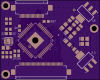
Loads of research later and here I am, totally going to miss the compo deadline but I've designed a PCB replacement for the PS2s onboard CXM4015AR graphics chip. This board is a development board which will allow me to test and further develop the scan doubler I'm building for the PS2 and once complete will feature everything required to simply replace the onboard IC with and get lovely, LCD friendly video.
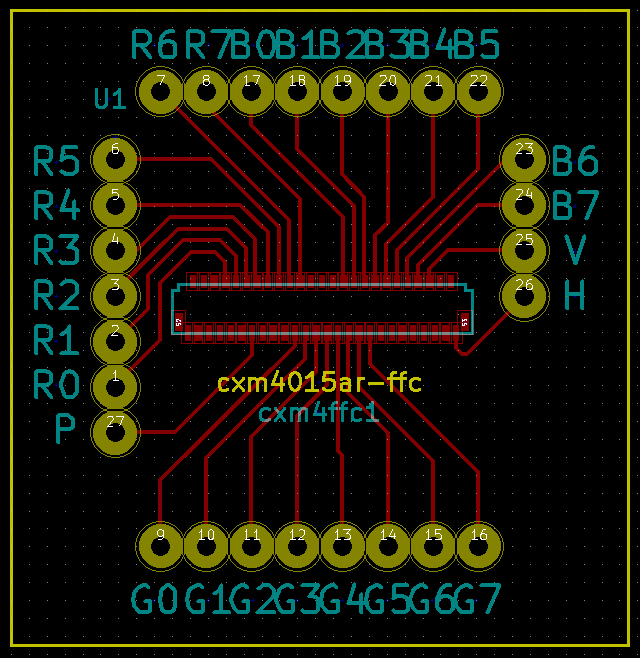
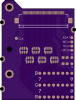
The first image is the daughter board which is linked via an FPC cable to the board in place of the graphics chip. I hope to get these sent to the PCB fab soon so I can carry on with the VHDL dev work to bring us some high quality PS2 displays! The end goal here is to house the entire scan doubler on the 16.2mm X 16.2mm IC board. The Max 10 FPGA is the one I'll be using thanks to @Herma for that recommendation.
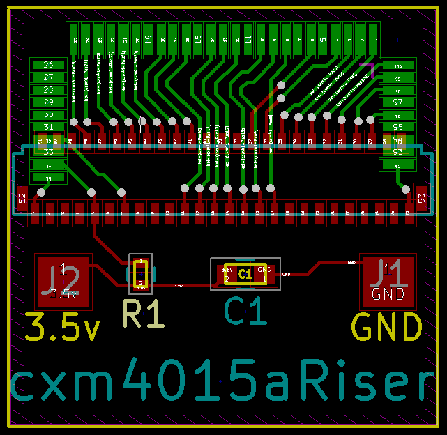
I'll have a couple versions available, all FPC cable based, 1 direct LVDS connection to the chip so no need for an LCD driver board at all, 1 VGA daughter board which will require an LCD driver board.
I'll be back with more news soon!
The first image is the daughter board which is linked via an FPC cable to the board in place of the graphics chip. I hope to get these sent to the PCB fab soon so I can carry on with the VHDL dev work to bring us some high quality PS2 displays! The end goal here is to house the entire scan doubler on the 16.2mm X 16.2mm IC board. The Max 10 FPGA is the one I'll be using thanks to @Herma for that recommendation.
I'll have a couple versions available, all FPC cable based, 1 direct LVDS connection to the chip so no need for an LCD driver board at all, 1 VGA daughter board which will require an LCD driver board.
I'll be back with more news soon!